EP2464073A2 - Empfänger und Übertragungsystem für ein Impulssignal - Google Patents
Empfänger und Übertragungsystem für ein Impulssignal Download PDFInfo
- Publication number
- EP2464073A2 EP2464073A2 EP11192358A EP11192358A EP2464073A2 EP 2464073 A2 EP2464073 A2 EP 2464073A2 EP 11192358 A EP11192358 A EP 11192358A EP 11192358 A EP11192358 A EP 11192358A EP 2464073 A2 EP2464073 A2 EP 2464073A2
- Authority
- EP
- European Patent Office
- Prior art keywords
- pulse signal
- pulse
- unit
- width
- deviation
- Prior art date
- Legal status (The legal status is an assumption and is not a legal conclusion. Google has not performed a legal analysis and makes no representation as to the accuracy of the status listed.)
- Granted
Links
Images




Classifications
-
- H—ELECTRICITY
- H04—ELECTRIC COMMUNICATION TECHNIQUE
- H04L—TRANSMISSION OF DIGITAL INFORMATION, e.g. TELEGRAPHIC COMMUNICATION
- H04L25/00—Baseband systems
- H04L25/38—Synchronous or start-stop systems, e.g. for Baudot code
- H04L25/40—Transmitting circuits; Receiving circuits
- H04L25/49—Transmitting circuits; Receiving circuits using code conversion at the transmitter; using predistortion; using insertion of idle bits for obtaining a desired frequency spectrum; using three or more amplitude levels ; Baseband coding techniques specific to data transmission systems
- H04L25/4902—Pulse width modulation; Pulse position modulation
-
- H—ELECTRICITY
- H04—ELECTRIC COMMUNICATION TECHNIQUE
- H04L—TRANSMISSION OF DIGITAL INFORMATION, e.g. TELEGRAPHIC COMMUNICATION
- H04L25/00—Baseband systems
- H04L25/02—Details ; arrangements for supplying electrical power along data transmission lines
- H04L25/03—Shaping networks in transmitter or receiver, e.g. adaptive shaping networks
- H04L25/03828—Arrangements for spectral shaping; Arrangements for providing signals with specified spectral properties
- H04L25/03834—Arrangements for spectral shaping; Arrangements for providing signals with specified spectral properties using pulse shaping
Definitions
- the present invention relates to a pulse signal receiving apparatus and a transmission system.
- digital signal transmission schemes may be divided broadly into a baseband scheme and a broadband scheme.
- the baseband scheme is a transmission scheme in which a digital signal is directly transmitted without being modulated.
- the broadband scheme is a transmission scheme in which a digital signal is modulated into an analog signal and the analog signal is transmitted.
- Representative transmission schemes for use in the broadband scheme may be a pulse width modulation (PWM) scheme, a pulse amplitude modulation (PAM) scheme, a pulse position modulation (PPM) scheme, and the like.
- the PWM or PPM scheme is usually used in the field of power control or motor control.
- the PWM or PPM scheme has also been used in infrared communication by an infrared data association (IrDa) standard, high-speed optical communication, and high-speed wireless communication of ultra wide band (UWB), because reduction of power consumption is possible and speeding up is facilitated.
- IrDa infrared data association
- UWB ultra wide band
- the PWM scheme is classified as either a single-edge modulation scheme or a double-edge modulation scheme.
- the single-edge modulation scheme is a modulation scheme in which either a period in which a pulse signal has a "high (H)” level or a period in which the pulse signal has a “low (L)” level is modulated.
- the double modulation scheme is a modulation scheme in which both the period in which the pulse signal has the "H” level and the period in which the pulse signal has the "L” level are modulated. If the double-edge modulation scheme is used, it is possible to implement higher performance (in terms of transmission rate, control responsiveness, or the like) as compared to when the single-edge modulation scheme is used.
- a difference between a pulse signal modulated by the single-edge scheme and a pulse signal modulated by the double-edge scheme is disclosed, for example, in Japanese Unexamined Patent Application, First Publication No. H9-84388 .
- a pulse edge defines an end time of a certain period (for example, a period of the "H" level) and a start time of a period following the period (for example, a period of the "L” level).
- a position of the pulse edge fluctuates due to noise or the like, a deviation (error) occurs in both periods before and after the pulse edge and a transmission error occurs.
- the transmission error increases due to an accumulated deviation.
- the present invention provides a pulse signal receiving apparatus and a transmission system capable of suppressing the occurrence of a transmission error due to the influence of noise.
- a pulse signal receiving apparatus may include: a reception unit that receives a pulse signal modulated by a double-edge modulation scheme; a measurement unit that measures an edge interval of the pulse signal, which has been received by the reception unit; a detection unit that detects a deviation of the edge interval, which has been measured by the measurement unit, for a pulse-width reference value indicating a reference value of a width of the pulse signal; a correction unit that corrects the edge interval, which is to be measured next by the measurement unit, by using the deviation, which has been detected by the detection unit; and a decoding unit that decodes the pulse signal, of which the edge interval has been corrected by the correction unit, so as to output a digital signal.
- the pulse signal receiving apparatus may further include: a holding unit that holds the deviation, which has been detected by the detection unit.
- the correction unit may correct the edge interval, which is to be measured next by the measurement unit, by using the deviation, which has been held in the holding unit.
- the measurement unit may include a timer for timing the edge interval of the pulse signal, which has been received by the reception unit.
- the correction unit may correct the edge interval, which is to be measured next by the measurement unit, by correcting an initial value of the timer by using the deviation, which has been detected by the detection unit.
- the reception unit may include: a filter unit that removes noise overlapping the received pulse signal; a shaping unit that shapes the received pulse signal; and an edge detecting unit that detects an edge position of the received pulse signal.
- a transmission system for transmitting a digital signal may include: a pulse signal transmitting apparatus that transmits a pulse signal, of which a pulse width has been modulated by a double-edge modulation scheme, according to a digital signal to be transmitted; and the pulse signal receiving apparatus that receives the pulse signal, which has been transmitted from the pulse signal transmitting apparatus, the pulse signal receiving apparatus decoding the received pulse signal into a digital signal.
- the transmission system may further include: a holding unit that holds the deviation, which has been detected by the detection unit.
- the correction unit may correct the edge interval, which is to be measured next by the measurement unit, by using the deviation, which has been held in the holding unit.
- the measurement unit may include a timer for timing the edge interval of the pulse signal, which has been received by the reception unit.
- the correction unit may correct the edge interval, which is to be measured next by the measurement unit, by correcting an initial value of the timer by using the deviation, which has been detected by the detection unit.
- the reception unit may include: a filter unit that removes noise overlapping the received pulse signal; a shaping unit that shapes the received pulse signal; and an edge detecting unit that detects an edge position of the received pulse signal.
- a pulse signal receiving method may include: receiving a pulse signal modulated by a double-edge modulation scheme; measuring an edge interval of the pulse signal, which has been received; detecting a deviation of the edge interval, which has been measured, for a pulse-width reference value indicating a reference value of a width of the pulse signal; correcting the edge interval, which is to be measured next, by using the deviation, which has been detected; and decoding the pulse signal, of which the edge interval has been corrected, so as to output a digital signal.
- the pulse signal receiving method may further include: holding the deviation, which has been detected; and correcting the edge interval, which is to be measured next, by using the deviation, which has been held.
- the pulse signal receiving method may further include: measuring the edge interval of the pulse signal, which has been received, by using a timer; and correcting the edge interval, which is to be measured next, by correcting an initial value of the timer by using the deviation, which has been detected.
- the pulse signal receiving method may further include: removing noise overlapping the received pulse signal; shaping the received pulse signal; and detecting an edge position of the received pulse signal.
- a measurement unit measures an edge interval of a pulse signal received by a reception unit
- a detection unit detects a deviation for a pulse-width reference value of the edge interval measured by the measurement unit
- a correction unit corrects the next edge interval that is measured by the measurement unit using the deviation detected by the detection unit.
- FIG 1 is a block diagram illustrating a configuration of main parts of a pulse signal receiving apparatus and a transmission system in accordance with the first preferred embodiment of the present invention.
- a transmission system 1 of the first preferred embodiment includes a pulse signal transmitting apparatus 10 and a pulse signal receiving apparatus 20 connected via a transmission cable C.
- a pulse signal PS is transmitted from the pulse signal transmitting apparatus 10 to the pulse signal receiving apparatus 20, so that a digital signal is transmitted.
- the pulse signal transmitting apparatus 10 includes a pulse-width encoding unit 11 and an output driver 12.
- the pulse signal transmitting apparatus 10 transmits the pulse signal PS of which a pulse width has been modulated by a double-edge modulation scheme to the pulse signal receiving apparatus 20 according to a digital signal D1 to be transmitted.
- the pulse-width encoding unit 11 generates the pulse signal to be transmitted to the pulse signal receiving apparatus 20 on the basis of the above-described digital signal D1. Specifically, a pulse signal having a length of a period in which a signal level is the "H" level and a length of a period in which the signal level is the "L” level modulated into pulse-width reference values corresponding to the digital signal D1 is generated.
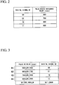
- FIG 2 is a diagram illustrating an example of a relationship between a digital signal to be transmitted and a pulse-width reference value in accordance with the first preferred embodiment of the present invention.
- a pulse-width reference value indicating a reference value of a width of a pulse signal is defined to be different according to a value of the digital signal D1 to be transmitted.
- pulse-width reference values including "600 nsec,” “700 nsec,” “800 nsec,” and “900 nsec” are defined for values “00,” “01,” “10,” and “11” of the digital signal D1, respectively.
- four types of pulse-width reference values when the digital signal D1 is 2 bits are illustrated in FIG 2 .
- the digital signal D1 is n bits (where n is an integer greater than or equal to 2), 2 n types of pulse-width reference values are defined.
- the pulse-width encoding unit 11 On the basis of the relationship described using FIG. 2 , the pulse-width encoding unit 11 generates a pulse signal by mutually modulating the length of the period in which the signal level is the "H” level and the length of the period in which the signal level is the "L” level according to the input digital signal D1.
- the output driver 12 transmits the pulse signal generated by the pulse-width encoding unit 11 to the transmission cable C as the pulse signal PS.
- the pulse signal receiving apparatus 20 includes a reception unit 21, a correction circuit unit 22, and a pulse-width decoding unit 23 (a decoding unit).
- the pulse signal receiving apparatus 20 receives the pulse signal PS transmitted from the pulse signal transmitting apparatus 10 via the transmission cable C, and decodes the pulse signal PS into a digital signal D2.
- the reception unit 21 includes a BPF 21a (a filter unit), an input receiver 21b (a shaping unit), and an edge detecting unit 21c.
- the reception unit 21 receives the pulse signal PS and outputs an edge detection signal indicating its edge position.
- the BPF 21a removes a noise component of a frequency band lower than a frequency band of the received pulse signal and a noise component of a frequency band higher than the frequency band of the received pulse signal.
- the input receiver 21b shapes a waveform of a pulse signal PS1 via the BPF 21 a.
- the edge detecting unit 21 c detects an edge position of a pulse signal PS2 of which a waveform is shaped by the input receiver 21 b, and outputs an edge detection signal indicating its detection result.
- the correction circuit unit 22 includes an edge interval measuring timer 22a (a measurement unit), a pulse-width correcting unit 22b (a correction unit), a pulse-width deviation detecting unit 22c (a detection unit), and a pulse-width deviation holding unit 22d (a holding unit).
- the correction circuit unit 22 measures a pulse width of the pulse signal PS (more accurately, an edge interval of the pulse signal PS2 of which the waveform has been shaped by the input receiver 21b), and corrects a deviation of the measured pulse width.
- the deviation of the pulse width means a variation amount (error) for the pulse-width reference value of the measured pulse width.
- the edge interval measuring timer 22a measures a pulse width that is an edge interval of the received pulse signal (the pulse signal PS2 of which the waveform has been shaped by the input receiver 21b). Furthermore, every time the pulse width is measured, the edge interval measuring timer 22a sets an initial value to "0" by clearing its measurement value (count value).
- the pulse-width correcting unit 22b corrects the pulse width measured by the edge interval measuring timer 22a using a pulse-width deviation held in the pulse-width deviation holding unit 22d.
- the pulse-width deviation detecting unit 22c detects a deviation between an output of the pulse-width correcting unit 22b and a pulse-width reference value V1 output from the pulse-width decoding unit 23.
- the output of the pulse-width correcting unit 22b is the pulse width measured by the edge interval measuring timer 22a or the pulse width measured by the edge interval measuring timer 22a corrected using the pulse-width deviation held in the pulse-width deviation holding unit 22d.
- the pulse-width reference value V1 output from the pulse-width decoding unit 23 is a pulse-width reference value corresponding to the output of the pulse-width correcting unit 22b.
- the pulse-width deviation detecting unit 22c detects a deviation for a pulse-width reference value of the pulse width measured by the edge interval measuring timer 22a (or the corrected pulse width).
- the pulse-width deviation holding unit 22d holds the pulse-width deviation detected by the pulse-width deviation detecting unit 22c until the next pulse-width deviation is output from the pulse-width deviation detecting unit 22c.
- the pulse-width decoding unit 23 decodes the digital signal D2 on the basis of the output of the pulse-width correcting unit 22b provided in the correction circuit unit 22, and outputs the pulse-width reference value V1 corresponding to the output of the pulse-width correcting unit 22b (corresponding to the decoded digital signal D2).
- FIG 3 is a diagram illustrating an example of a relationship between a pulse width of a received pulse signal and a digital signal to be decoded in accordance with the first preferred embodiment of the present invention.
- a plurality of determination areas which do not overlap a pulse width output from the pulse-width correcting unit 22b provided in the correction circuit unit 22, are set, and the digital signal D2 to be decoded is allocated to each of the determination areas.
- a first determination area R1 of 550 ⁇ W ⁇ 650, a second determination area R2 of 650 ⁇ W ⁇ 750, a third determination area R3 of 750 ⁇ W ⁇ 850, and a fourth determination area R4 of 850 ⁇ W ⁇ 950 are set for a pulse width W [nsec] output from the pulse-width correcting unit 22b.
- Values "00,” “01,” “10,” and “11” of the digital signal D2 are allocated to the above-described first to fourth determination areas R1 to R4, respectively. Furthermore, when the pulse width W is less than 550 [nsec] or when the pulse width W is greater than or equal to 950 [nsec], a "bit error" is defined. Thus, for example, when the output of the pulse-width correcting unit 22b indicates a pulse width of 940 [nsec], the pulse-width decoding unit 23 outputs the value "11" of the digital signal D2 and outputs a pulse-width reference value [900] corresponding to the digital signal D2 as the pulse-width reference value V1.
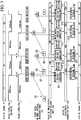
- FIG 4 is a timing chart illustrating a signal to be transmitted by the transmission system in accordance with the first preferred embodiment of the present invention.
- a pulse signal PS in which a length of a period of a first "H” level is "900 nsec,” a length of a period of an “L” level continuous thereto is “700 nsec,” a length of a period of the “H” level continuous thereto is “800 nsec,” and a length of a period of the "L” level continuous thereto is “600 nsec” is generated and transmitted to the transmission cable C.
- This pulse signal PS is propagated to the pulse signal receiving apparatus 20 through the transmission cable C.
- the pulse signal PS is affected by an extraneous noise component N illustrated in FIG 4 while the pulse signal PS is propagated through the transmission cable C. Then, the pulse signal PS overlapping the noise component N is received by the reception unit 21 of the pulse signal receiving apparatus 20, and a pulse signal PS1 indicated by a solid line in FIG 4 is output from the BPF 21a. Furthermore, for a comparison, a pulse signal PS1 output from the BPF 21 a when the influence of the noise component N is absent is indicated by a dashed line in FIG 4 .
- the same pulse signal PS2 as the pulse signal PS transmitted from the pulse signal transmitting apparatus 10 to the transmission cable C is output from the input receiver 21b provided in the reception unit 21. That is, the pulse signal PS2 of which the pulse width varies in the order of "900 nsec,” “700 nsec,” “800 nsec,” and “600 nsec” is output.
- a pulse signal PS2 in which an initial period is lengthened and varied to "940 nsec,” a second period is shortened and varied to "640 nsec,” and a fourth period is also varied to "620 nsec" is output from the input receiver 21b provided in the reception unit 21.
- pulse widths sequentially measured by the edge interval measuring timer 22a provided in the correction circuit unit 22 of the pulse signal receiving apparatus 20 are equal to "900 nsec,” “700 nsec,” “800 nsec,” and “600 nsec.”
- the pulse-width deviation detected by the pulse-width deviation detecting unit 22c of the correction circuit unit 22 becomes "0.”
- the pulse width measured by the edge interval measuring timer 22a is output to the pulse-width decoding unit 23 without being corrected by the pulse-width correcting unit 22b, and the digital signal D2 including "11,” “01,” “10,” and “00” identical with the digital signal D1 is output from the pulse-width decoding unit 23.
- the pulse width measured by the edge interval measuring timer 22a provided in the correction circuit unit 22 may be varied from the pulse-width reference value.
- the pulse signal receiving apparatus 20 of the first preferred embodiment suppresses the occurrence of a transmission error even when the noise component N overlaps the pulse signal PS transmitted from the pulse signal transmitting apparatus 10 by correcting the variation (deviation) as described above in the correction circuit unit 22.
- an operation of the pulse signal receiving apparatus 20 when the pulse signal PS overlapping the noise component N has been received will be described in detail.
- FIG 5 is a diagram illustrating the operation of the pulse signal receiving apparatus in accordance with the first preferred embodiment of the present invention.
- a count operation of the edge interval measuring timer 22a is initiated (step S1). If the next edge detection signal is output from the reception unit 21 while the count operation of the edge interval measuring timer 22a is performed, the count operation of the edge interval measuring timer 22a is stopped and its count value (a count value indicating a pulse width "940 nsec") is output to the pulse-width correcting unit 22b (step S2). Furthermore, if a count value is output from the edge interval measuring timer 22a, the count value is cleared and the count operation is resumed after the initial value is set to "0" (step S3).
- the pulse-width correcting unit 22b corrects the input count value using a pulse-width deviation held in the pulse-width deviation holding unit 22d (step S4). As illustrated in FIG 5 , because an initial value of the pulse-width deviation held in the pulse-width deviation holding unit 22d is "0," an output of the pulse-width correcting unit 22b becomes a value indicating the pulse width "940 nsec" measured by the edge interval measuring timer 22a. The output of the pulse-width correcting unit 22b is input to the pulse-width decoding unit 23 and decoded into a digital signal D2 including "11" (step S5).
- the pulse-width decoding unit 23 outputs the digital signal D2 including "11.”
- the pulse-width reference value "900" corresponding to the digital signal D2 including “11” is output from the pulse-width decoding unit 23 as the pulse-width reference value V1 (step S6).
- the pulse-width deviation detecting unit 22c detects a deviation between the output of the pulse-width correcting unit 22b and the pulse-width reference value V1 output from the pulse-width decoding unit 23 (step S7), and the deviation "+40" is held in the pulse-width deviation holding unit 22d.
- step S8 If the next edge detection signal is output from the reception unit 21 to the edge interval measuring timer 22a, the count operation of the edge interval measuring timer 22a is stopped and its count value (a count value indicating a pulse width "640 nsec") is output to the pulse-width correcting unit 22b (step S8). Furthermore, if a count value is output from the edge interval measuring timer 22a, the count value is re-cleared and the count operation is resumed after the initial value is set to "0" (step S9).
- the pulse-width correcting unit 22b corrects the input count value using a pulse-width deviation held in the pulse-width deviation holding unit 22d (step S10). As illustrated in FIG 5 , because the pulse-width deviation "+40" is held in the pulse-width deviation holding unit 22d, an output of the pulse-width correcting unit 22b becomes a value "680 nsec” obtained by adding the deviation "+40" to the pulse width "640 nsec" measured by the edge interval measuring timer 22a. The output of the pulse-width correcting unit 22b is input to the pulse-width decoding unit 23 and decoded into a digital signal D2 including "01" from the relationship illustrated in FIG 3 (step S11).
- the pulse-width reference value "700" corresponding to the digital signal D2 including "01” is output from the pulse-width decoding unit 23 as the pulse-width reference value V1 (step S12).
- the pulse-width deviation detecting unit 22c detects a deviation between the output of the pulse-width correcting unit 22b and the pulse-width reference value V1 output from the pulse-width decoding unit 23 (step S13), and the deviation "-20" is held in the pulse-width deviation holding unit 22d.
- the pulse signal receiving apparatus 20 obtains the digital signal D2 including "11,” “01,” “10,” and “00” identical with the output digital signal D2 when the influence of the noise component N is absent (or the digital signal D2 identical with the digital signal D1), so that it can be seen that no transmission error occurs even when there is the influence of the noise component N.
- the pulse width (edge interval) of the pulse signal PS2 received by the reception unit 21 is measured, a deviation for a pulse-width reference value of the measured pulse width is detected and held, and the next pulse width that is measured is corrected using the held deviation, so that fluctuations of front and rear pulse widths are canceled out.
- FIG 6 is a block diagram illustrating a configuration of main parts of a pulse signal receiving apparatus in accordance with the second preferred embodiment of the present invention.
- the pulse signal receiving apparatus 30 of the second preferred embodiment includes a correction circuit unit 31 in place of the correction circuit unit 22 of the pulse signal receiving apparatus 20 illustrated in FIG 1 .
- the correction circuit unit 31 includes the edge interval measuring timer 22a and the pulse-width deviation detecting unit 22c provided in the correction circuit unit 22, a pulse-width holding unit 31a, and a timer initial value setting unit 31b (a correction unit).
- the pulse-width holding unit 31a holds a pulse width output from the edge interval measuring timer 22a until the next pulse width is output from the edge interval measuring timer 22a.
- the timer initial value setting unit 31b sets an initial value of the edge interval measuring timer 22a using a deviation detected by the pulse-width deviation detecting unit 22c.
- the pulse-width deviation holding unit 22d holds the deviation detected by the pulse-width deviation detecting unit 22c and the pulse-width correcting unit 22b corrects the next pulse width that is measured by the edge interval measuring timer 22a according to the held deviation.
- the timer initial value setting unit 31b corrects an initial value of the edge interval measuring timer 22a using the deviation detected by the pulse-width deviation detecting unit 22c and the next pulse width that is measured by the edge interval measuring timer 22a is corrected according to the corrected initial value.
- FIG 7 is a diagram illustrating the operation of the pulse signal receiving apparatus in accordance with the second preferred embodiment of the present invention.
- a count operation of the edge interval measuring timer 22a is initiated (step S21). If the next edge detection signal is output from the reception unit 21, the count operation of the edge interval measuring timer 22a is stopped and its count value (a count value indicating a pulse width "940 nsec") is output and held in the pulse-width holding unit 31a (step S22).
- a pulse width held in the pulse-width holding unit 31a is output to the pulse-width decoding unit 23 and decoded into a digital signal D2 including "11” (step S23).
- the pulse-width reference value "900" corresponding to the digital signal D2 including “11” is output from the pulse-width decoding unit 23 as the pulse-width reference value V1 (step S24).
- the pulse-width deviation detecting unit 22c detects a deviation between the output of the pulse-width holding unit 31a and the pulse-width reference value V1 output from the pulse-width decoding unit 23 (step S25), and the deviation "+40" is set to an initial value of the edge interval measuring timer 22a by the timer initial value setting unit 31b (step S26).
- the initial value is set, the count operation of the edge interval measuring timer 22a is resumed.
- step S27 If the next edge detection signal is output from the reception unit 21 to the edge interval measuring timer 22a, the count operation of the edge interval measuring timer 22a is stopped and its count value is output and held in the pulse-width holding unit 31a (step S27).
- the count value counted by the edge interval measuring timer 22a originally indicates a pulse width "640 nsec.”
- the initial value is set to "+40” in the above-described process of step S26, the count value held in the pulse-width holding unit 31a becomes "680 nsec" obtained by adding the deviation "+40" to the pulse width "640 nsec.”
- the pulse width held in the pulse-width holding unit 31a is output to the pulse-width decoding unit 23 and decoded into the digital signal D2 including "01" (step S28).
- the pulse-width reference value "700” corresponding to the digital signal D2 including "01” is output from the pulse-width decoding unit 23 as the pulse-width reference value V1 (step S29).
- the pulse-width deviation detecting unit 22c detects a deviation between the output of the pulse-width holding unit 3 1 a and the pulse-width reference value V1 output from the pulse-width decoding unit 23 (step S30), and the deviation "-20" is set to the initial value of the edge interval measuring timer 22a by the timer initial value setting unit 31b (step S31). If the initial value is set, the count operation of the edge interval measuring timer 22a is resumed.
- the pulse signal receiving apparatus 30 obtains the digital signal D2 including "11,” “01,” “10,” and “00” identical with the output digital signal D2 when the influence of the noise component N is absent (or the digital signal D2 identical with the digital signal D1), so that it can be seen that no transmission error occurs even when there is the influence of the noise component N.
- the pulse width (edge interval) of the pulse signal PS2 received by the reception unit 21 is measured, a deviation for a pulse-width reference value of the measured pulse width is detected, an initial value of the edge interval measuring timer 22a is corrected using the deviation, and the next pulse width that is measured is corrected, so that fluctuations of front and rear pulse widths are canceled out.
- the present invention is not limited to the above-described preferred embodiments and free changes are possible within the scope of the present invention.
- the correction circuit units 22 and 31, the pulse-width decoding unit 23, and so on of the pulse signal receiving apparatuses 20 and 30 are constituted by hardware has been described in the above-described preferred embodiment, these may be implemented by software.
- a 2-bit digital signal D1 is transmitted has been described for simplicity of description in the above-described preferred embodiments.
- the number of bits of the digital signal D1 to be transmitted is not limited to 2, and it is possible to transmit a digital signal D1 having any number of bits.
- a pulse-width reference value indicating a reference signal of a width of a pulse signal is set to a linearly variable value has been described in the above-described preferred embodiment.
- the pulse-width reference value may be set to a non-linearly variable value.
- unit is used to describe a component, section or part of a hardware and/or software that is constructed and/or programmed to carry out the desired function.
- Typical examples of the hardware may include, but are not limited to, a device and a circuit.
Landscapes
- Engineering & Computer Science (AREA)
- Physics & Mathematics (AREA)
- Spectroscopy & Molecular Physics (AREA)
- Computer Networks & Wireless Communication (AREA)
- Signal Processing (AREA)
- Power Engineering (AREA)
- Dc Digital Transmission (AREA)
- Digital Transmission Methods That Use Modulated Carrier Waves (AREA)
- Arrangements For Transmission Of Measured Signals (AREA)
Applications Claiming Priority (1)
| Application Number | Priority Date | Filing Date | Title |
|---|---|---|---|
| JP2010274949A JP5218535B2 (ja) | 2010-12-09 | 2010-12-09 | パルス信号受信装置及び伝送システム |
Publications (3)
| Publication Number | Publication Date |
|---|---|
| EP2464073A2 true EP2464073A2 (de) | 2012-06-13 |
| EP2464073A3 EP2464073A3 (de) | 2012-08-22 |
| EP2464073B1 EP2464073B1 (de) | 2019-03-06 |
Family
ID=45560634
Family Applications (1)
| Application Number | Title | Priority Date | Filing Date |
|---|---|---|---|
| EP11192358.7A Not-in-force EP2464073B1 (de) | 2010-12-09 | 2011-12-07 | Empfänger und Übertragungsystem für ein Impulssignal |
Country Status (5)
| Country | Link |
|---|---|
| US (1) | US8660172B2 (de) |
| EP (1) | EP2464073B1 (de) |
| JP (1) | JP5218535B2 (de) |
| CN (1) | CN102571117B (de) |
| SG (1) | SG182074A1 (de) |
Families Citing this family (10)
| Publication number | Priority date | Publication date | Assignee | Title |
|---|---|---|---|---|
| KR101997894B1 (ko) * | 2012-03-19 | 2019-07-08 | 삼성전자주식회사 | Fm-uwb 통신 시스템에서 전력소모를 줄이기 위한 송수신 장치 |
| DE102013209309A1 (de) * | 2013-05-21 | 2014-11-27 | Zf Friedrichshafen Ag | Verfahren und Schaltung zur Bewertung pulsweitenmodulierter Signale |
| EP3367187A4 (de) * | 2015-10-21 | 2019-06-19 | Tendyron Corporation | Kommunikationsausrüstung, adaptervorrichtung und kommunikationssystem |
| JP2017103548A (ja) * | 2015-11-30 | 2017-06-08 | ラピスセミコンダクタ株式会社 | 送信装置、受信装置、通信システム及び通信方法 |
| JP7135657B2 (ja) * | 2018-09-25 | 2022-09-13 | 株式会社デンソー | 車両制御装置 |
| CN109142820B (zh) * | 2018-09-26 | 2021-07-13 | 深圳市鼎阳科技股份有限公司 | 一种脉冲波发生装置 |
| US11797463B2 (en) * | 2020-12-25 | 2023-10-24 | Nidec Corporation | Signal generation device |
| US11962306B2 (en) * | 2021-06-29 | 2024-04-16 | Nvidia Corporation | Clock anomaly detection |
| US12079028B2 (en) * | 2022-01-31 | 2024-09-03 | Nvidia Corporation | Fast clock detection |
| JP2025121030A (ja) * | 2024-02-06 | 2025-08-19 | 株式会社アイシン | 制御装置 |
Citations (1)
| Publication number | Priority date | Publication date | Assignee | Title |
|---|---|---|---|---|
| JPH0984388A (ja) | 1995-09-11 | 1997-03-28 | Nissan Motor Co Ltd | 交流モータの制御装置 |
Family Cites Families (10)
| Publication number | Priority date | Publication date | Assignee | Title |
|---|---|---|---|---|
| JPS55143826A (en) * | 1979-04-26 | 1980-11-10 | Mitsubishi Electric Corp | Pulse modulation system |
| JPS63148743A (ja) * | 1986-12-11 | 1988-06-21 | Casio Comput Co Ltd | 差分バイフエ−ズ復調方法 |
| JP3063376B2 (ja) * | 1992-04-16 | 2000-07-12 | 株式会社デンソー | Pwm信号通信装置 |
| US6169765B1 (en) * | 1997-05-28 | 2001-01-02 | Integration Associates, Inc. | Apparatus and method for output signal pulse width error correction in a communications receiver |
| JPH1168862A (ja) * | 1997-08-11 | 1999-03-09 | Nissan Motor Co Ltd | 通信装置 |
| JP3705183B2 (ja) * | 2000-12-28 | 2005-10-12 | 株式会社デンソー | データ受信装置 |
| DE10138218B4 (de) * | 2001-08-03 | 2004-01-22 | Atmel Germany Gmbh | Verfahren zur Übertragung von Daten |
| JP4347003B2 (ja) * | 2003-09-10 | 2009-10-21 | セイコープレシジョン株式会社 | 時刻情報検出方法、時刻情報検出装置および電波修正時計 |
| US7554332B2 (en) * | 2006-03-10 | 2009-06-30 | Advantest Corporation | Calibration apparatus, calibration method, testing apparatus, and testing method |
| JP5109668B2 (ja) * | 2007-03-09 | 2012-12-26 | セイコーエプソン株式会社 | 受信装置および受信方法 |
-
2010
- 2010-12-09 JP JP2010274949A patent/JP5218535B2/ja not_active Expired - Fee Related
-
2011
- 2011-12-07 US US13/313,887 patent/US8660172B2/en not_active Expired - Fee Related
- 2011-12-07 CN CN201110404383.5A patent/CN102571117B/zh not_active Expired - Fee Related
- 2011-12-07 EP EP11192358.7A patent/EP2464073B1/de not_active Not-in-force
- 2011-12-07 SG SG2011090628A patent/SG182074A1/en unknown
Patent Citations (1)
| Publication number | Priority date | Publication date | Assignee | Title |
|---|---|---|---|---|
| JPH0984388A (ja) | 1995-09-11 | 1997-03-28 | Nissan Motor Co Ltd | 交流モータの制御装置 |
Also Published As
| Publication number | Publication date |
|---|---|
| JP2012124783A (ja) | 2012-06-28 |
| CN102571117B (zh) | 2015-02-18 |
| SG182074A1 (en) | 2012-07-30 |
| US20120155524A1 (en) | 2012-06-21 |
| US8660172B2 (en) | 2014-02-25 |
| JP5218535B2 (ja) | 2013-06-26 |
| CN102571117A (zh) | 2012-07-11 |
| EP2464073B1 (de) | 2019-03-06 |
| EP2464073A3 (de) | 2012-08-22 |
Similar Documents
| Publication | Publication Date | Title |
|---|---|---|
| EP2464073B1 (de) | Empfänger und Übertragungsystem für ein Impulssignal | |
| US7920601B2 (en) | Vehicular communications system having improved serial communication | |
| WO1999038265A1 (en) | Method and device for detecting rate | |
| EP2639155A3 (de) | Verfahren und Vorrichtung zur drahtlosen Datenübertragung, die periodischen Signalblockaden ausgesetzt wird | |
| EP4243316A3 (de) | Verfahren und vorrichtung zum senden und empfangen eines drahtlosen aufweckpakets | |
| CN109964412A (zh) | 一种多通道校正装置、幅度校正方法、相位校正方法、收发系统和基站 | |
| JP2013192107A5 (de) | ||
| EP3041297A1 (de) | Verfahren und vorrichtung zur einstellung einer übertragungsleistung | |
| CN114611542B (zh) | 信号降噪处理方法及通信装置 | |
| CN106856588B (zh) | 蓝牙设备的频点选取方法及装置 | |
| US9973368B2 (en) | Fine timing | |
| KR100813864B1 (ko) | 주파수 도약 타이밍 동기 획득 시스템 | |
| AU759254B2 (en) | Data transmission method and data transmission device | |
| US9112763B1 (en) | Device, system and method for bi-phase modulation decoding | |
| US10050724B2 (en) | Communication system | |
| RU147413U1 (ru) | Устройство адаптивной коррекции с обратной связью по решению | |
| US8390484B2 (en) | Method and apparatus for decoding transmitted/received data | |
| EP2530864A1 (de) | Vorrichtung und Verfahren zum Stromsparen | |
| JP2008109513A (ja) | Fsk受信装置 | |
| KR101496323B1 (ko) | 확장 맨체스터 코드, 이를 이용한 부호화 장치 및 이를 이용하여 부호화된 신호의 클럭 및 데이터 복구 방법 및 장치 | |
| KR101773993B1 (ko) | 에러 보상 방법 및 그 방법을 이용하는 송수신 시스템 | |
| JP2010268364A (ja) | 狭帯域デジタル無線通信装置および群遅延歪みを等化するためのパラメータ設定方法 | |
| US7184479B2 (en) | Data transmission method and data transmission device | |
| JP2007201626A (ja) | 受信機 | |
| JP4946623B2 (ja) | デジタル無線機の受信部 |
Legal Events
| Date | Code | Title | Description |
|---|---|---|---|
| PUAI | Public reference made under article 153(3) epc to a published international application that has entered the european phase |
Free format text: ORIGINAL CODE: 0009012 |
|
| AK | Designated contracting states |
Kind code of ref document: A2 Designated state(s): AL AT BE BG CH CY CZ DE DK EE ES FI FR GB GR HR HU IE IS IT LI LT LU LV MC MK MT NL NO PL PT RO RS SE SI SK SM TR |
|
| AX | Request for extension of the european patent |
Extension state: BA ME |
|
| PUAL | Search report despatched |
Free format text: ORIGINAL CODE: 0009013 |
|
| AK | Designated contracting states |
Kind code of ref document: A3 Designated state(s): AL AT BE BG CH CY CZ DE DK EE ES FI FR GB GR HR HU IE IS IT LI LT LU LV MC MK MT NL NO PL PT RO RS SE SI SK SM TR |
|
| AX | Request for extension of the european patent |
Extension state: BA ME |
|
| RIC1 | Information provided on ipc code assigned before grant |
Ipc: H04L 25/49 20060101AFI20120719BHEP |
|
| 17P | Request for examination filed |
Effective date: 20130220 |
|
| 17Q | First examination report despatched |
Effective date: 20130327 |
|
| STAA | Information on the status of an ep patent application or granted ep patent |
Free format text: STATUS: EXAMINATION IS IN PROGRESS |
|
| GRAP | Despatch of communication of intention to grant a patent |
Free format text: ORIGINAL CODE: EPIDOSNIGR1 |
|
| STAA | Information on the status of an ep patent application or granted ep patent |
Free format text: STATUS: GRANT OF PATENT IS INTENDED |
|
| INTG | Intention to grant announced |
Effective date: 20180914 |
|
| GRAS | Grant fee paid |
Free format text: ORIGINAL CODE: EPIDOSNIGR3 |
|
| GRAA | (expected) grant |
Free format text: ORIGINAL CODE: 0009210 |
|
| STAA | Information on the status of an ep patent application or granted ep patent |
Free format text: STATUS: THE PATENT HAS BEEN GRANTED |
|
| AK | Designated contracting states |
Kind code of ref document: B1 Designated state(s): AL AT BE BG CH CY CZ DE DK EE ES FI FR GB GR HR HU IE IS IT LI LT LU LV MC MK MT NL NO PL PT RO RS SE SI SK SM TR |
|
| REG | Reference to a national code |
Ref country code: GB Ref legal event code: FG4D |
|
| RIN1 | Information on inventor provided before grant (corrected) |
Inventor name: YOSHIDA, YOSHIO Inventor name: KIHARA, NORIAKI |
|
| REG | Reference to a national code |
Ref country code: CH Ref legal event code: EP Ref country code: AT Ref legal event code: REF Ref document number: 1106089 Country of ref document: AT Kind code of ref document: T Effective date: 20190315 |
|
| REG | Reference to a national code |
Ref country code: DE Ref legal event code: R096 Ref document number: 602011056825 Country of ref document: DE |
|
| REG | Reference to a national code |
Ref country code: IE Ref legal event code: FG4D |
|
| REG | Reference to a national code |
Ref country code: NL Ref legal event code: MP Effective date: 20190306 |
|
| REG | Reference to a national code |
Ref country code: LT Ref legal event code: MG4D |
|
| PG25 | Lapsed in a contracting state [announced via postgrant information from national office to epo] |
Ref country code: FI Free format text: LAPSE BECAUSE OF FAILURE TO SUBMIT A TRANSLATION OF THE DESCRIPTION OR TO PAY THE FEE WITHIN THE PRESCRIBED TIME-LIMIT Effective date: 20190306 Ref country code: NO Free format text: LAPSE BECAUSE OF FAILURE TO SUBMIT A TRANSLATION OF THE DESCRIPTION OR TO PAY THE FEE WITHIN THE PRESCRIBED TIME-LIMIT Effective date: 20190606 Ref country code: SE Free format text: LAPSE BECAUSE OF FAILURE TO SUBMIT A TRANSLATION OF THE DESCRIPTION OR TO PAY THE FEE WITHIN THE PRESCRIBED TIME-LIMIT Effective date: 20190306 Ref country code: LT Free format text: LAPSE BECAUSE OF FAILURE TO SUBMIT A TRANSLATION OF THE DESCRIPTION OR TO PAY THE FEE WITHIN THE PRESCRIBED TIME-LIMIT Effective date: 20190306 |
|
| PG25 | Lapsed in a contracting state [announced via postgrant information from national office to epo] |
Ref country code: HR Free format text: LAPSE BECAUSE OF FAILURE TO SUBMIT A TRANSLATION OF THE DESCRIPTION OR TO PAY THE FEE WITHIN THE PRESCRIBED TIME-LIMIT Effective date: 20190306 Ref country code: GR Free format text: LAPSE BECAUSE OF FAILURE TO SUBMIT A TRANSLATION OF THE DESCRIPTION OR TO PAY THE FEE WITHIN THE PRESCRIBED TIME-LIMIT Effective date: 20190607 Ref country code: NL Free format text: LAPSE BECAUSE OF FAILURE TO SUBMIT A TRANSLATION OF THE DESCRIPTION OR TO PAY THE FEE WITHIN THE PRESCRIBED TIME-LIMIT Effective date: 20190306 Ref country code: BG Free format text: LAPSE BECAUSE OF FAILURE TO SUBMIT A TRANSLATION OF THE DESCRIPTION OR TO PAY THE FEE WITHIN THE PRESCRIBED TIME-LIMIT Effective date: 20190606 Ref country code: LV Free format text: LAPSE BECAUSE OF FAILURE TO SUBMIT A TRANSLATION OF THE DESCRIPTION OR TO PAY THE FEE WITHIN THE PRESCRIBED TIME-LIMIT Effective date: 20190306 Ref country code: RS Free format text: LAPSE BECAUSE OF FAILURE TO SUBMIT A TRANSLATION OF THE DESCRIPTION OR TO PAY THE FEE WITHIN THE PRESCRIBED TIME-LIMIT Effective date: 20190306 |
|
| REG | Reference to a national code |
Ref country code: AT Ref legal event code: MK05 Ref document number: 1106089 Country of ref document: AT Kind code of ref document: T Effective date: 20190306 |
|
| PG25 | Lapsed in a contracting state [announced via postgrant information from national office to epo] |
Ref country code: SK Free format text: LAPSE BECAUSE OF FAILURE TO SUBMIT A TRANSLATION OF THE DESCRIPTION OR TO PAY THE FEE WITHIN THE PRESCRIBED TIME-LIMIT Effective date: 20190306 Ref country code: RO Free format text: LAPSE BECAUSE OF FAILURE TO SUBMIT A TRANSLATION OF THE DESCRIPTION OR TO PAY THE FEE WITHIN THE PRESCRIBED TIME-LIMIT Effective date: 20190306 Ref country code: CZ Free format text: LAPSE BECAUSE OF FAILURE TO SUBMIT A TRANSLATION OF THE DESCRIPTION OR TO PAY THE FEE WITHIN THE PRESCRIBED TIME-LIMIT Effective date: 20190306 Ref country code: IT Free format text: LAPSE BECAUSE OF FAILURE TO SUBMIT A TRANSLATION OF THE DESCRIPTION OR TO PAY THE FEE WITHIN THE PRESCRIBED TIME-LIMIT Effective date: 20190306 Ref country code: EE Free format text: LAPSE BECAUSE OF FAILURE TO SUBMIT A TRANSLATION OF THE DESCRIPTION OR TO PAY THE FEE WITHIN THE PRESCRIBED TIME-LIMIT Effective date: 20190306 Ref country code: PT Free format text: LAPSE BECAUSE OF FAILURE TO SUBMIT A TRANSLATION OF THE DESCRIPTION OR TO PAY THE FEE WITHIN THE PRESCRIBED TIME-LIMIT Effective date: 20190706 Ref country code: ES Free format text: LAPSE BECAUSE OF FAILURE TO SUBMIT A TRANSLATION OF THE DESCRIPTION OR TO PAY THE FEE WITHIN THE PRESCRIBED TIME-LIMIT Effective date: 20190306 Ref country code: AL Free format text: LAPSE BECAUSE OF FAILURE TO SUBMIT A TRANSLATION OF THE DESCRIPTION OR TO PAY THE FEE WITHIN THE PRESCRIBED TIME-LIMIT Effective date: 20190306 |
|
| PG25 | Lapsed in a contracting state [announced via postgrant information from national office to epo] |
Ref country code: PL Free format text: LAPSE BECAUSE OF FAILURE TO SUBMIT A TRANSLATION OF THE DESCRIPTION OR TO PAY THE FEE WITHIN THE PRESCRIBED TIME-LIMIT Effective date: 20190306 Ref country code: SM Free format text: LAPSE BECAUSE OF FAILURE TO SUBMIT A TRANSLATION OF THE DESCRIPTION OR TO PAY THE FEE WITHIN THE PRESCRIBED TIME-LIMIT Effective date: 20190306 |
|
| REG | Reference to a national code |
Ref country code: DE Ref legal event code: R097 Ref document number: 602011056825 Country of ref document: DE |
|
| PG25 | Lapsed in a contracting state [announced via postgrant information from national office to epo] |
Ref country code: AT Free format text: LAPSE BECAUSE OF FAILURE TO SUBMIT A TRANSLATION OF THE DESCRIPTION OR TO PAY THE FEE WITHIN THE PRESCRIBED TIME-LIMIT Effective date: 20190306 Ref country code: IS Free format text: LAPSE BECAUSE OF FAILURE TO SUBMIT A TRANSLATION OF THE DESCRIPTION OR TO PAY THE FEE WITHIN THE PRESCRIBED TIME-LIMIT Effective date: 20190706 |
|
| PLBE | No opposition filed within time limit |
Free format text: ORIGINAL CODE: 0009261 |
|
| STAA | Information on the status of an ep patent application or granted ep patent |
Free format text: STATUS: NO OPPOSITION FILED WITHIN TIME LIMIT |
|
| PG25 | Lapsed in a contracting state [announced via postgrant information from national office to epo] |
Ref country code: DK Free format text: LAPSE BECAUSE OF FAILURE TO SUBMIT A TRANSLATION OF THE DESCRIPTION OR TO PAY THE FEE WITHIN THE PRESCRIBED TIME-LIMIT Effective date: 20190306 |
|
| 26N | No opposition filed |
Effective date: 20191209 |
|
| PG25 | Lapsed in a contracting state [announced via postgrant information from national office to epo] |
Ref country code: SI Free format text: LAPSE BECAUSE OF FAILURE TO SUBMIT A TRANSLATION OF THE DESCRIPTION OR TO PAY THE FEE WITHIN THE PRESCRIBED TIME-LIMIT Effective date: 20190306 |
|
| PG25 | Lapsed in a contracting state [announced via postgrant information from national office to epo] |
Ref country code: TR Free format text: LAPSE BECAUSE OF FAILURE TO SUBMIT A TRANSLATION OF THE DESCRIPTION OR TO PAY THE FEE WITHIN THE PRESCRIBED TIME-LIMIT Effective date: 20190306 |
|
| REG | Reference to a national code |
Ref country code: CH Ref legal event code: PL |
|
| REG | Reference to a national code |
Ref country code: BE Ref legal event code: MM Effective date: 20191231 |
|
| PG25 | Lapsed in a contracting state [announced via postgrant information from national office to epo] |
Ref country code: MC Free format text: LAPSE BECAUSE OF FAILURE TO SUBMIT A TRANSLATION OF THE DESCRIPTION OR TO PAY THE FEE WITHIN THE PRESCRIBED TIME-LIMIT Effective date: 20190306 |
|
| GBPC | Gb: european patent ceased through non-payment of renewal fee |
Effective date: 20191207 |
|
| PG25 | Lapsed in a contracting state [announced via postgrant information from national office to epo] |
Ref country code: GB Free format text: LAPSE BECAUSE OF NON-PAYMENT OF DUE FEES Effective date: 20191207 Ref country code: LU Free format text: LAPSE BECAUSE OF NON-PAYMENT OF DUE FEES Effective date: 20191207 Ref country code: IE Free format text: LAPSE BECAUSE OF NON-PAYMENT OF DUE FEES Effective date: 20191207 |
|
| PG25 | Lapsed in a contracting state [announced via postgrant information from national office to epo] |
Ref country code: BE Free format text: LAPSE BECAUSE OF NON-PAYMENT OF DUE FEES Effective date: 20191231 Ref country code: CH Free format text: LAPSE BECAUSE OF NON-PAYMENT OF DUE FEES Effective date: 20191231 Ref country code: LI Free format text: LAPSE BECAUSE OF NON-PAYMENT OF DUE FEES Effective date: 20191231 |
|
| PG25 | Lapsed in a contracting state [announced via postgrant information from national office to epo] |
Ref country code: CY Free format text: LAPSE BECAUSE OF FAILURE TO SUBMIT A TRANSLATION OF THE DESCRIPTION OR TO PAY THE FEE WITHIN THE PRESCRIBED TIME-LIMIT Effective date: 20190306 |
|
| PG25 | Lapsed in a contracting state [announced via postgrant information from national office to epo] |
Ref country code: HU Free format text: LAPSE BECAUSE OF FAILURE TO SUBMIT A TRANSLATION OF THE DESCRIPTION OR TO PAY THE FEE WITHIN THE PRESCRIBED TIME-LIMIT; INVALID AB INITIO Effective date: 20111207 Ref country code: MT Free format text: LAPSE BECAUSE OF FAILURE TO SUBMIT A TRANSLATION OF THE DESCRIPTION OR TO PAY THE FEE WITHIN THE PRESCRIBED TIME-LIMIT Effective date: 20190306 Ref country code: FR Free format text: LAPSE BECAUSE OF NON-PAYMENT OF DUE FEES Effective date: 20191231 |
|
| PG25 | Lapsed in a contracting state [announced via postgrant information from national office to epo] |
Ref country code: MK Free format text: LAPSE BECAUSE OF FAILURE TO SUBMIT A TRANSLATION OF THE DESCRIPTION OR TO PAY THE FEE WITHIN THE PRESCRIBED TIME-LIMIT Effective date: 20190306 |
|
| P01 | Opt-out of the competence of the unified patent court (upc) registered |
Effective date: 20230603 |
|
| PGFP | Annual fee paid to national office [announced via postgrant information from national office to epo] |
Ref country code: DE Payment date: 20231121 Year of fee payment: 13 |
|
| REG | Reference to a national code |
Ref country code: DE Ref legal event code: R119 Ref document number: 602011056825 Country of ref document: DE |
|
| PG25 | Lapsed in a contracting state [announced via postgrant information from national office to epo] |
Ref country code: DE Free format text: LAPSE BECAUSE OF NON-PAYMENT OF DUE FEES Effective date: 20250701 |