EP2465425B1 - Leitung für ein aktives implantierbares medizinisches Gerät, umfassend einen Chip, insbesondere zum Multiplexen - Google Patents
Leitung für ein aktives implantierbares medizinisches Gerät, umfassend einen Chip, insbesondere zum Multiplexen Download PDFInfo
- Publication number
- EP2465425B1 EP2465425B1 EP20110182241 EP11182241A EP2465425B1 EP 2465425 B1 EP2465425 B1 EP 2465425B1 EP 20110182241 EP20110182241 EP 20110182241 EP 11182241 A EP11182241 A EP 11182241A EP 2465425 B1 EP2465425 B1 EP 2465425B1
- Authority
- EP
- European Patent Office
- Prior art keywords
- support tube
- probe
- chip
- conductive
- sheath
- Prior art date
- Legal status (The legal status is an assumption and is not a legal conclusion. Google has not performed a legal analysis and makes no representation as to the accuracy of the status listed.)
- Active
Links
Images


Classifications
-
- A—HUMAN NECESSITIES
- A61—MEDICAL OR VETERINARY SCIENCE; HYGIENE
- A61B—DIAGNOSIS; SURGERY; IDENTIFICATION
- A61B5/00—Measuring for diagnostic purposes; Identification of persons
- A61B5/02—Detecting, measuring or recording for evaluating the cardiovascular system, e.g. pulse, heart rate, blood pressure or blood flow
- A61B5/021—Measuring pressure in heart or blood vessels
- A61B5/0215—Measuring pressure in heart or blood vessels by means inserted into the body
-
- A—HUMAN NECESSITIES
- A61—MEDICAL OR VETERINARY SCIENCE; HYGIENE
- A61B—DIAGNOSIS; SURGERY; IDENTIFICATION
- A61B5/00—Measuring for diagnostic purposes; Identification of persons
- A61B5/24—Detecting, measuring or recording bioelectric or biomagnetic signals of the body or parts thereof
- A61B5/25—Bioelectric electrodes therefor
- A61B5/271—Arrangements of electrodes with cords, cables or leads, e.g. single leads or patient cord assemblies
- A61B5/273—Connection of cords, cables or leads to electrodes
-
- A—HUMAN NECESSITIES
- A61—MEDICAL OR VETERINARY SCIENCE; HYGIENE
- A61B—DIAGNOSIS; SURGERY; IDENTIFICATION
- A61B5/00—Measuring for diagnostic purposes; Identification of persons
- A61B5/68—Arrangements of detecting, measuring or recording means, e.g. sensors, in relation to patient
- A61B5/6846—Arrangements of detecting, measuring or recording means, e.g. sensors, in relation to patient specially adapted to be brought in contact with an internal body part, i.e. invasive
- A61B5/6847—Arrangements of detecting, measuring or recording means, e.g. sensors, in relation to patient specially adapted to be brought in contact with an internal body part, i.e. invasive mounted on an invasive device
- A61B5/686—Permanently implanted devices, e.g. pacemakers, other stimulators, biochips
-
- A—HUMAN NECESSITIES
- A61—MEDICAL OR VETERINARY SCIENCE; HYGIENE
- A61N—ELECTROTHERAPY; MAGNETOTHERAPY; RADIATION THERAPY; ULTRASOUND THERAPY
- A61N1/00—Electrotherapy; Circuits therefor
- A61N1/02—Details
- A61N1/04—Electrodes
- A61N1/05—Electrodes for implantation or insertion into the body, e.g. heart electrode
-
- A—HUMAN NECESSITIES
- A61—MEDICAL OR VETERINARY SCIENCE; HYGIENE
- A61N—ELECTROTHERAPY; MAGNETOTHERAPY; RADIATION THERAPY; ULTRASOUND THERAPY
- A61N1/00—Electrotherapy; Circuits therefor
- A61N1/02—Details
- A61N1/04—Electrodes
- A61N1/05—Electrodes for implantation or insertion into the body, e.g. heart electrode
- A61N1/0587—Epicardial electrode systems; Endocardial electrodes piercing the pericardium
-
- H—ELECTRICITY
- H01—ELECTRIC ELEMENTS
- H01R—ELECTRICALLY-CONDUCTIVE CONNECTIONS; STRUCTURAL ASSOCIATIONS OF A PLURALITY OF MUTUALLY-INSULATED ELECTRICAL CONNECTING ELEMENTS; COUPLING DEVICES; CURRENT COLLECTORS
- H01R43/00—Apparatus or processes specially adapted for manufacturing, assembling, maintaining, or repairing of line connectors or current collectors or for joining electric conductors
- H01R43/20—Apparatus or processes specially adapted for manufacturing, assembling, maintaining, or repairing of line connectors or current collectors or for joining electric conductors for assembling or disassembling contact members with insulating base, case or sleeve
-
- A—HUMAN NECESSITIES
- A61—MEDICAL OR VETERINARY SCIENCE; HYGIENE
- A61B—DIAGNOSIS; SURGERY; IDENTIFICATION
- A61B2562/00—Details of sensors; Constructional details of sensor housings or probes; Accessories for sensors
- A61B2562/12—Manufacturing methods specially adapted for producing sensors for in-vivo measurements
- A61B2562/125—Manufacturing methods specially adapted for producing sensors for in-vivo measurements characterised by the manufacture of electrodes
-
- A—HUMAN NECESSITIES
- A61—MEDICAL OR VETERINARY SCIENCE; HYGIENE
- A61B—DIAGNOSIS; SURGERY; IDENTIFICATION
- A61B5/00—Measuring for diagnostic purposes; Identification of persons
- A61B5/12—Audiometering
- A61B5/121—Audiometering evaluating hearing capacity
- A61B5/125—Audiometering evaluating hearing capacity objective methods
-
- A—HUMAN NECESSITIES
- A61—MEDICAL OR VETERINARY SCIENCE; HYGIENE
- A61B—DIAGNOSIS; SURGERY; IDENTIFICATION
- A61B8/00—Diagnosis using ultrasonic, sonic or infrasonic waves
- A61B8/06—Measuring blood flow
-
- Y—GENERAL TAGGING OF NEW TECHNOLOGICAL DEVELOPMENTS; GENERAL TAGGING OF CROSS-SECTIONAL TECHNOLOGIES SPANNING OVER SEVERAL SECTIONS OF THE IPC; TECHNICAL SUBJECTS COVERED BY FORMER USPC CROSS-REFERENCE ART COLLECTIONS [XRACs] AND DIGESTS
- Y10—TECHNICAL SUBJECTS COVERED BY FORMER USPC
- Y10S—TECHNICAL SUBJECTS COVERED BY FORMER USPC CROSS-REFERENCE ART COLLECTIONS [XRACs] AND DIGESTS
- Y10S439/00—Electrical connectors
- Y10S439/909—Medical use or attached to human body
-
- Y—GENERAL TAGGING OF NEW TECHNOLOGICAL DEVELOPMENTS; GENERAL TAGGING OF CROSS-SECTIONAL TECHNOLOGIES SPANNING OVER SEVERAL SECTIONS OF THE IPC; TECHNICAL SUBJECTS COVERED BY FORMER USPC CROSS-REFERENCE ART COLLECTIONS [XRACs] AND DIGESTS
- Y10—TECHNICAL SUBJECTS COVERED BY FORMER USPC
- Y10T—TECHNICAL SUBJECTS COVERED BY FORMER US CLASSIFICATION
- Y10T29/00—Metal working
- Y10T29/49—Method of mechanical manufacture
- Y10T29/49002—Electrical device making
- Y10T29/49117—Conductor or circuit manufacturing
- Y10T29/49124—On flat or curved insulated base, e.g., printed circuit, etc.
- Y10T29/4913—Assembling to base an electrical component, e.g., capacitor, etc.
- Y10T29/49146—Assembling to base an electrical component, e.g., capacitor, etc. with encapsulating, e.g., potting, etc.
-
- Y—GENERAL TAGGING OF NEW TECHNOLOGICAL DEVELOPMENTS; GENERAL TAGGING OF CROSS-SECTIONAL TECHNOLOGIES SPANNING OVER SEVERAL SECTIONS OF THE IPC; TECHNICAL SUBJECTS COVERED BY FORMER USPC CROSS-REFERENCE ART COLLECTIONS [XRACs] AND DIGESTS
- Y10—TECHNICAL SUBJECTS COVERED BY FORMER USPC
- Y10T—TECHNICAL SUBJECTS COVERED BY FORMER US CLASSIFICATION
- Y10T29/00—Metal working
- Y10T29/49—Method of mechanical manufacture
- Y10T29/49002—Electrical device making
- Y10T29/49117—Conductor or circuit manufacturing
- Y10T29/49169—Assembling electrical component directly to terminal or elongated conductor
-
- Y—GENERAL TAGGING OF NEW TECHNOLOGICAL DEVELOPMENTS; GENERAL TAGGING OF CROSS-SECTIONAL TECHNOLOGIES SPANNING OVER SEVERAL SECTIONS OF THE IPC; TECHNICAL SUBJECTS COVERED BY FORMER USPC CROSS-REFERENCE ART COLLECTIONS [XRACs] AND DIGESTS
- Y10—TECHNICAL SUBJECTS COVERED BY FORMER USPC
- Y10T—TECHNICAL SUBJECTS COVERED BY FORMER US CLASSIFICATION
- Y10T29/00—Metal working
- Y10T29/49—Method of mechanical manufacture
- Y10T29/49002—Electrical device making
- Y10T29/49117—Conductor or circuit manufacturing
- Y10T29/49169—Assembling electrical component directly to terminal or elongated conductor
- Y10T29/49171—Assembling electrical component directly to terminal or elongated conductor with encapsulating
Definitions
- the invention relates generally to the field of "active medical devices” as defined by the Council of European Communities Directive 93/42 / EC of 14 June 1993, and in particular "active implantable medical devices” as defined by Council Directive 90/385 / EEC of 20 June 1990.
- This definition includes in particular the devices responsible for monitoring cardiac activity and generating pacing, resynchronization, defibrillation and / or cardioversion pulses in the event of arrhythmia detected by the device. It also includes neurological devices, medical substance delivery pumps, cochlear implants, implanted biological sensors, as well as pH or intracorporeal impedance measuring devices (such as trans-pulmonary impedance or impedance measurement). intracardiac).
- these active implantable medical devices use electrodes integrated in a probe, itself connected to the generator of the device.
- these electrodes are intended to come into contact with the tissues to be stimulated or those on which it is desired to collect an electrical signal: myocardium, nerve, muscle.
- these electrodes may be endocavitary electrodes (placed in a myocardial cavity in contact with the wall thereof), epicardial (in particular to define a reference potential, or to apply a shock), or intravascular (the probe is for example introduced into the coronary sinus to a location facing the wall of the left ventricle).
- a first aspect of the development of these devices is the multiplication of the number of electrodes, especially for the so-called “multisite” devices that allow to choose the sites of stimulation / detection optimizing the operation of the device.
- the multiplication of the electrodes can also result from the presence on the same level of the probe of several sectoral electrodes (electrodes directed specifically in a radial direction with respect to the probe, at the stimulation site), with the possibility of selecting one or the other. other of these sectoral electrodes to optimize the delivery of pulses to the chosen site.
- This is particularly the case of implanted probes in the venous coronary network, intended for the indirect stimulation of a left cavity: with several sectoral electrodes, it is easy to choose the one that is turned towards the wall of the epicardium, facing the cavity, and in contact with this wall and thus avoid stimulation of the phrenic nerve.
- EA endocardial acceleration
- probe sensors also require a specific link for the transmission of signals from the sensor, located at the distal end of the probe, to the generator connected to the opposite, proximal end.
- This connection specific to the sensor is superadded specific links already existing between the generator and the various electrodes located in the distal region of the probe.
- the EP 1 938 861 A1 and the EP 2 082 684 A1 (both in the name of ELA Medical) describe such a probe provided with a plurality of electrodes near its distal end, for example ten electrodes, associated with a chip, hermetically encapsulated in the vicinity of the electrodes in a ring rigid, multiplexing / demultiplexing the electrodes with a common bus formed by two conductors isolated along the entire length of the probe to the proximal connector for coupling with the generator, the latter being equipped with a homologous demultiplexing / multiplexing circuit.
- WO 2010/091435 A2 and WO 2006/069322 A2 (Proteus Biomedical, Inc.) describe a system in which a common two-wire bus carries signals to and from addressable sectoral electrodes formed on "satellites" carried by the probe at regular intervals.
- the described construction leaves for the probe only an inner lumen of much smaller diameter than the outer diameter, because of the size of the chip and connections to the son. This constraint limits the application of such a technique to electrodes located at the end of the probe, because otherwise the small diameter of the light would not allow the use of conventional laying techniques, unless strongly increase the outer diameter of the probe at the location of the electrodes, which would limit the applications.
- this production technology is extremely difficult to implement and its reliability over time has not been proven.
- the invention proposes for this purpose a probe of the known type disclosed in particular by the WO 2010/091435 A2 above, comprising: an elongated flexible sheath with a central lumen; at least one conductive connection housed in the sheath lumen; a rigid cylindrical support tube of insulating material, with a central bore through, the sheath being interrupted by the support tube which is interposed on the sheath so that its bore is coaxial with the sheath of light, the support tube having a cavity forming chip receptacle, opening into a central region of the support tube at the surface thereof; at least one sensing / stimulating electrode carried by the support tube at the surface of the sheath; and at least one electronic circuit, comprising on a substrate a chip and at least two conductive contact pads connected respectively to the conductive connection and to the electrode, the chip being disposed with a curved conformation in the receptacle of the support tube, the chip carrying on one side of the substrate an outer conductive pad and on the opposite side an inner
- the chip substrate is a flexible substrate
- the conductive connection housed by the sheath has a discontinuity at the location of the support tube
- the bushing conductor is a conductive strip formed on the surface of the tube. support, it extends in the axial direction along it, and it is connected at each of its ends to the conductive connection vis-à-vis housed in the sheath.
- the chip is a chip on flexible substrate, carrying on one side of the substrate an outer conductive pad and on the opposite side an inner conductive pad, and this chip is disposed with a curved conformation in the receptacle of the support tube.
- the sensing / stimulating electrode is carried by the support tube and is electrically connected to the outer conductive pad of the chip.
- the band conductive it is connected (i) at each of its ends, the conductive connection vis-à-vis housed in the sheath, and (ii) in a central region, the inner conductive pad of the chip.
- the Figure 8 represents the part of the characteristic probe of the invention with its various constituent elements, as obtained after execution of the various illustrated manufacturing steps Figures 1 to 7 .
- the reference 10 generally designates the body of a known general type of probe, of which only a portion, generally located in the vicinity of the distal ends, bears a collection and / or stimulation electrode. , this electrode being an annular electrode in the illustrated example Figures 1 to 8 (and a plurality of sectoral electrodes in the illustrated example Figures 9 to 11 , described below).
- the probe includes two conductive connections in the form of an individually insulated spiral wire, each of the two links for example consisting of a respective pair of conductors 12, 12 and 14, 14. These conductive links run the entire length of the probe and are connected distally to a coupling connector to an implant generator (not shown).
- the probe also carries an annular electrode 16 connected to a chip 18 providing the multiplexing / demultiplexing of this electrode (as well as other electrodes located at other points of the probe) with the conductive links 12, 14 acting as link bus between the various electrodes of the probe and the remote generator.
- the chip 18 is thus electrically connected, on the one hand, to the electrode 16 and, on the other hand, to each of the two conductive links 12 and 14.
- the chip 18 is here described in the form of an electrode multiplexer / demultiplexer (s), but the invention is not limited to this type of circuit: the chip 18 may also be coupled to a sensor (i.e., a signal transducer for producing an electrical signal as a function of variations of a physical parameter), or even incorporate such a sensor, or may comprise an electronic circuit active such as amplifier, filter associated or not with a sensor disposed in proximity, or an electromechanical microsystem (MEMS), or generally any active element technologically integrable in a probe body.
- a sensor i.e., a signal transducer for producing an electrical signal as a function of variations of a physical parameter
- MEMS electromechanical microsystem
- the chip comprises two outputs corresponding to the two conductive links 12 and 14 of the two-wire bus, and a corresponding third output the connection to the electrode 16, and possibly additional outputs in the case for example of a multi-electrode configuration (as in the case of Figures 9 to 11 which will be described below, comprising a plurality of sectoral electrodes multiplexed by the same chip).
- the chip is mounted on a rigid cylindrical support tube 20 made of insulating material, comprising a central through bore 22 making it possible to ensure, without reducing the diameter, the continuity of the internal light of the probe, which is necessary. for example the passage of a mandrel or a grommet during installation.
- the chip is a flexible substrate type chip, that is to say whose substrate is sufficiently thinned to be curved and marry the cylindrical surface of the support.
- This technique is for example described by Zimmermann et al., A Seamless Ultra-Thin Chip Fabrication and Assembly Process, Electron Devices Meeting IEDM '06, 11-13 Dec. 2006, pp. 1-3 .
- To make the chip flexible it is necessary to thin its substrate (generally a silicon substrate) to a thickness of less than 0.1 mm so that it can match the shape of the tube, whose outer diameter is, in the illustrated example, 0.85 mm where the chip is located.
- the chip carries on its external (convex) surface an external conductive pad 24 intended to come into contact with the electrode 16, and it carries at its opposite (concave) surface two diametrically opposite internal conductive pads 26 (only one of these pads 26). being visible in the figures), intended to be connected, in the manner described below, to the two respective conductive links 12 and 14.
- These various conductive areas comprise for example a gold alloy which can be brazed by reflow to 450 ° C to establish the electrical connections required with the elements just mentioned.
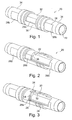
- the Figures 1 and 2 show, in isolation, the support tube 20 before it receives the flexible chip (the Figure 2 is a broken view of the Figure 1 , showing in section the internal structure of the tube).
- This tube is a tube of electrically insulating material, made by overmolding plastic material or by assembling ceramic components secured by high temperature reflow or gluing. It carries two elongated conductive strips 28, diametrically opposite (only one of these bands being visible in the figures) formed at the surface and extending in the axial direction over most of the length of the tube so as to form a crossing, with an apparent central region 28a and two end regions 28b.
- the support tube comprises a central region 30 of greater diameter, for example 1 mm, provided with a cavity 32 forming a receptacle for the flexible chip.
- the depth of this cavity corresponds substantially to the thickness of the chip so that it, when it is put in place, will be flush with the contour of the cavity (as illustrated Figure 3 ).
- the configuration of the tube is such that the central portion 28a of the traversing band 28 is visible at the bottom of the cavity 32.
- the support tube also comprises two end regions 34 of smaller diameter, for example 0.85 mm in the example shown, carrying the two respective ends 28b of the conductive strip through 28.
- the length of the tube is, for example order of 5 mm and the receptacle surface of the order of 1 to 2 mm 2 .
- central bore 22 is on the totally isolated electrical plane of the bushing strips 28 and of the cavity 32, thanks to a wall thickness 36 (FIG. Figure 2 ) of the support tube, which preserves the electrical insulation while maintaining a relatively large bore diameter, of the order of 0.55 mm.
- the Figure 3 illustrates the support tube after transfer of the chip 18 into the cavity 32.
- the next step consists in threading on the previously obtained assembly a sleeve 38 of conductive material, fitted on the central part of the support tube 20 and resting on all the extent, in the axial direction, of the cavity 32, so that this sleeve 38 covers the entire surface of the chip 18.
- a thermal reflow step makes it possible to establish the electrical connection between each of the inner conductive pads 26 of the chip and the central portion 28a of the conducting conductor strip 28, thus making it possible to ensure electrical continuity between each of these ranges and the two ends 28b parents of 28 at the ends 34 of the support tube 20.
- This heating also makes it possible to establish the electrical contact between the outer region 24 of the chip 18 and the conductive material of the sleeve 38, intended to constitute the annular electrode 16.
- the next step, illustrated Figure 5 consists in perfect sealing of the assembly with respect to the external environment, by injecting a mass 40 of material, for example polyurethane glue, into the gap between the sleeve 38 and the central region 30 of the tube support 20.
- a mass 40 of material for example polyurethane glue
- this mass of adhesive protects the assembly, and in particular the chip 18, with respect to all external mechanical stresses and stresses, thus ensuring a protective and durable encapsulation of all electrical and electronic components, including during assembly of the probe at the factory.
- the assembly obtained is ready for a visual inspection, a test of the electrical functionalities before assembly on the probe body that will now be described.
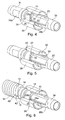
- the next step, illustrated Figure 6 consists in setting up electrical connections formed by the spiral conductors 12, 12 and 14, 14 and in soldering the conductors of each of these links to the corresponding area 28b, for example by means of a laser weld 42, 42 between the stripped end of the conductors 12,12 and the end region 28b proximal of the bushing conductor located there.
- the same weld is made in the diametrically opposed region (not visible in the figure) between the conductors 14, 14 of the other electrical connection and the other conductive crossing strip diametrically opposite to that visible on the Figure 6 .
- the next step, illustrated Figure 7 is to perform the same operation on the opposite side of the annular sleeve 38, that is to say distal side, for example by laser welding 44,44 conductors 12,12 on the end 28b distal side of the conductive strip of passage 28 (and in the same way for the conductors 14,14 in the diametrically opposite region).
- the final step, illustrated Figure 8 consists in coating the spiral conductors 12, 12 and 14, 14 on either side of the sleeve 38, with a cylindrical insulated sheath, for example made of polyurethane or silicone, of a constant diameter, identical to that of the sleeve 38.
- a cylindrical insulated sheath for example made of polyurethane or silicone, of a constant diameter, identical to that of the sleeve 38.
- a probe of the monodiameter type with a typical outside diameter of 1.6 mm (4.8 French) identical to that of conventional probes, for example an Xfine TX26D type probe manufactured by Sorin CRM, Clamart, France, and provided with an internal lumen 22 at least 0.55 mm (diameter of the central bore of the support tube 20).
- FIGs 9 to 11 illustrate a variant in which the conductive sleeve 38 which formed the annular electrode 16 of the previous embodiment is replaced by an insulating sleeve 48 of the same diameter, but provided with a plurality of cavities 50, for example four cavities 50 axially oriented, each revealing an outer conductive area 24 of the chip 18.
- a plurality of sectorial electrodes for example oriented in four quadrants, these electrodes being selectable at will at means of a multiplexing system integrated in the chip 18.
- the latter is therefore provided with a plurality of external conductive pads 24, in number equal to that of the sectoral electrodes, these ranges remaining apparent at the bottom of the cavities 50 of the sleeve 48 after placing it on the support tube 20 ( Figure 10 ).
- the sectoral electrodes 52 are formed for example by clipping a conductive micromechanical component coming into contact with the outer conductive pad 24 of the chip 18, and whose outer surface (which is flush with the cylindrical sleeve 48) constitutes the actual sectoral electrode.
- each of the sectoral electrodes it is easy to adjust the surface and the shape of each of the sectoral electrodes, simply by defining in a desired way the dimensions and the shape of the cavities 50 of the insulating sleeve 48.
Landscapes
- Health & Medical Sciences (AREA)
- Life Sciences & Earth Sciences (AREA)
- Heart & Thoracic Surgery (AREA)
- Engineering & Computer Science (AREA)
- Veterinary Medicine (AREA)
- Public Health (AREA)
- General Health & Medical Sciences (AREA)
- Animal Behavior & Ethology (AREA)
- Biomedical Technology (AREA)
- Cardiology (AREA)
- Surgery (AREA)
- Medical Informatics (AREA)
- Molecular Biology (AREA)
- Pathology (AREA)
- Biophysics (AREA)
- Physics & Mathematics (AREA)
- Nuclear Medicine, Radiotherapy & Molecular Imaging (AREA)
- Radiology & Medical Imaging (AREA)
- Physiology (AREA)
- Vascular Medicine (AREA)
- Manufacturing & Machinery (AREA)
- Electrotherapy Devices (AREA)
- Measurement And Recording Of Electrical Phenomena And Electrical Characteristics Of The Living Body (AREA)
Claims (6)
- Sonde für eine aktive implantierbare medizinische Vorrichtung, die Folgendes aufweist:- eine längliche flexible Hülle (10) mit einem zentralen Langloch;- mindestens eine leitende Verbindung (12, 14), die im Langloch der Hülle untergebracht ist;- ein steifes zylindrisches Tragrohr (20) aus Isoliermaterial mit einer zentralen Durchgangsbohrung (22), wobei die Hülle durch das Tragrohr unterbrochen wird, das so auf die Hülle zwischengeschoben wird, dass seine Bohrung mit dem Langloch der Hülle koaxial ist,- wobei das Tragrohr einen Hohlraum aufweist, der einen Aufnahmebehälter (32) für einen Chip formt, der in einer zentralen Zone (30) des Tragrohrs an dessen Oberfläche mündet;- mindestens eine Erfassungs-/Stimulationselektrode (16; 52), die vom Tragrohr (20) im Bereich der Oberfläche der Hülle getragen wird; und- mindestens eine elektronische Schaltung, die auf einem Substrat einen Chip (18) und mindestens zwei leitende Kontaktbereiche (26, 24) aufweist, die mit der leitenden Verbindung bzw. mit der Elektrode verbunden sind, wobei der Chip mit einer gekrümmten Gestaltung im Aufnahmebehälter (32) des Tragrohrs angeordnet ist,
wobei der Chip (18) auf einer Seite des Substrats einen äußeren leitenden Bereich (24) und auf der gegenüberliegenden Seite einen inneren leitenden Bereich (26) trägt, wobei die Erfassungs-/Stimulationselektrode (16; 52) elektrisch mit dem äußeren leitenden Bereich (24) des Chips verbunden ist; und- einen Durchgangsleiter (28), der in einer zentralen Zone (28a) mit dem inneren leitenden Bereich (26) des Chips verbunden ist,wobei die Sonde dadurch gekennzeichnet ist, dass:- das Substrat des Chips (18) ein flexibles Substrat ist,- die in der Hülle untergebrachte leitende Verbindung eine Unterbrechung an der Stelle des Tragrohrs aufweist; und- der Durchgangsleiter ein leitendes Band (28) ist, das an der Oberfläche des Tragrohrs geformt ist, es erstreckt sich in axialer Richtung entlang von diesem, und es ist an jedem seiner Enden (28b) mit der gegenüberliegenden leitenden Verbindung (12) verbunden, die in der Hülle untergebracht ist. - Sonde nach Anspruch 1, bei der das Isoliermaterial des Tragrohrs ein Keramikmaterial ist.
- Sonde nach Anspruch 1, die eine einzige Ringelektrode in Form einer leitenden Muffe (16) aufweist, die sich in Umfangsrichtung auf dem ganzen Umfang des Tragrohrs erstreckt und auf dessen zentrale Zone (30) aufgeschoben ist.
- Sonde nach Anspruch 1, die eine Vielzahl von Sektorelektroden (52) aufweist, die voneinander isoliert, in Umfangsrichtung auf dem Umfang des Tragrohrs verteilt und je mit einer entsprechenden Vielzahl von äußeren leitenden Bereichen (24) des Chips verbunden sind.
- Sonde nach Anspruch 1, bei der der Gesamtdurchmesser der Sonde in der Zone des Tragrohrs und der Elektrode konstant und gleich dem Durchmesser der flexiblen Hülle ist.
- Sonde nach Anspruch 1, die zwei unterschiedliche leitende Verbindungen (12, 14) aufweist, die im Langloch der Hülle untergebracht sind, wobei das Tragrohr zwei entsprechende unterschiedliche leitende Durchgangsbänder (28) aufweist, die zueinander isoliert und in diametral entgegengesetzten Zonen des Tragrohrs geformt sind.
Applications Claiming Priority (1)
| Application Number | Priority Date | Filing Date | Title |
|---|---|---|---|
| FR1060452 | 2010-12-14 |
Publications (2)
| Publication Number | Publication Date |
|---|---|
| EP2465425A1 EP2465425A1 (de) | 2012-06-20 |
| EP2465425B1 true EP2465425B1 (de) | 2013-01-23 |
Family
ID=44312298
Family Applications (1)
| Application Number | Title | Priority Date | Filing Date |
|---|---|---|---|
| EP20110182241 Active EP2465425B1 (de) | 2010-12-14 | 2011-09-21 | Leitung für ein aktives implantierbares medizinisches Gerät, umfassend einen Chip, insbesondere zum Multiplexen |
Country Status (2)
| Country | Link |
|---|---|
| US (3) | US9020574B2 (de) |
| EP (1) | EP2465425B1 (de) |
Families Citing this family (6)
| Publication number | Priority date | Publication date | Assignee | Title |
|---|---|---|---|---|
| EP2465425B1 (de) * | 2010-12-14 | 2013-01-23 | Sorin CRM SAS | Leitung für ein aktives implantierbares medizinisches Gerät, umfassend einen Chip, insbesondere zum Multiplexen |
| JP6229077B2 (ja) * | 2014-07-11 | 2017-11-08 | ボストン サイエンティフィック サイムド,インコーポレイテッドBoston Scientific Scimed,Inc. | アブレーション医療デバイス |
| US10603484B2 (en) | 2014-11-25 | 2020-03-31 | Medtronic Bakken Research Center B.V. | System and method for neurostimulation and/or neurorecording |
| EP3075411B1 (de) | 2015-04-03 | 2017-10-25 | Sorin CRM SAS | Multielektrodensonde mit multiplex-steuerung, insbesondere zur herzstimulation, und entsprechendes anschlussverfahren |
| EP3170574B1 (de) | 2015-11-19 | 2022-07-13 | Heraeus Deutschland GmbH & Co. KG | Verfahren zur herstellung einer hülse für eine elektrode für medizinische anwendungen |
| CN108463265B (zh) | 2016-01-19 | 2021-06-01 | 圣犹达医疗用品心脏病学部门有限公司 | 无损伤连接件和采用该无损伤连接件的导管 |
Family Cites Families (24)
| Publication number | Priority date | Publication date | Assignee | Title |
|---|---|---|---|---|
| US4628934A (en) * | 1984-08-07 | 1986-12-16 | Cordis Corporation | Method and means of electrode selection for pacemaker with multielectrode leads |
| US5046503A (en) * | 1989-04-26 | 1991-09-10 | Advanced Cardiovascular Systems, Inc. | Angioplasty autoperfusion catheter flow measurement method and apparatus |
| US5535752A (en) * | 1995-02-27 | 1996-07-16 | Medtronic, Inc. | Implantable capacitive absolute pressure and temperature monitor system |
| FR2796562B1 (fr) * | 1996-04-04 | 2005-06-24 | Medtronic Inc | Techniques de stimulation d'un tissu vivant et d'enregistrement avec commande locale de sites actifs |
| US6076012A (en) * | 1996-12-19 | 2000-06-13 | Ep Technologies, Inc. | Structures for supporting porous electrode elements |
| US6248080B1 (en) * | 1997-09-03 | 2001-06-19 | Medtronic, Inc. | Intracranial monitoring and therapy delivery control device, system and method |
| US6123675A (en) * | 1998-10-06 | 2000-09-26 | Trex Medical Corporation | Temperature gradient sensing probe for monitoring hyperthermic medical treatments |
| FR2790966B1 (fr) | 1999-03-17 | 2001-05-04 | Ela Medical Sa | Sonde de stimulation de l'oreillette gauche implantable dans le reseau veineux coronarien pour dispositif medical implantable actif, notamment stimulateur de type "multisite" |
| DE19930265A1 (de) * | 1999-06-25 | 2000-12-28 | Biotronik Mess & Therapieg | Elektrodenanordnung |
| WO2002058551A2 (en) * | 2001-01-22 | 2002-08-01 | Integrated Sensing Systems, Inc. | Wireless mems capacitive sensor for physiologic parameter measurement |
| US7194919B2 (en) * | 2003-05-29 | 2007-03-27 | Transonic Systems, Inc. | Acoustically coupled ultrasonic transit time flow sensors |
| US7930037B2 (en) * | 2003-09-30 | 2011-04-19 | Medtronic, Inc. | Field steerable electrical stimulation paddle, lead system, and medical device incorporating the same |
| US8948836B2 (en) * | 2003-12-26 | 2015-02-03 | Medtronic Minimed, Inc. | Implantable apparatus for sensing multiple parameters |
| US20080255647A1 (en) * | 2004-12-22 | 2008-10-16 | Marc Jensen | Implantable Addressable Segmented Electrodes |
| US20080077186A1 (en) * | 2006-04-18 | 2008-03-27 | Proteus Biomedical, Inc. | High phrenic, low capture threshold pacing devices and methods |
| JP4111523B2 (ja) * | 2004-12-27 | 2008-07-02 | 岩手県 | 家畜用胚移植器 |
| US20080114230A1 (en) * | 2006-11-14 | 2008-05-15 | Bruce Addis | Electrode support |
| FR2910818A1 (fr) | 2006-12-28 | 2008-07-04 | Ela Medical Soc Par Actions Si | Circuit de commutation controlee d'electrodes multiplexees, pour un dispositf medical implantable actif |
| EP2082684B1 (de) | 2008-01-25 | 2009-12-16 | Ela Medical | Aktives medizinisches Implantat, das bidirektionelle Kommunikationsmittel zwischen einem Generator und Sensoren oder Stellgliedern umfasst, die sich am Ende einer Sonde befinden |
| JP4452750B2 (ja) * | 2008-05-22 | 2010-04-21 | 並木精密宝石株式会社 | センサエレメント、センサシステム、カテーテルおよびセンサエレメントの製造方法 |
| JP2012508624A (ja) * | 2008-11-13 | 2012-04-12 | プロテウス バイオメディカル インコーポレイテッド | 多重化複数電極神経刺激装置 |
| US20120035684A1 (en) | 2009-02-09 | 2012-02-09 | Todd Thompson | Multiplexed, Multi-Electrode Neurostimulation Devices with Integrated Circuits Having Integrated Electrodes |
| US8744548B2 (en) * | 2009-06-10 | 2014-06-03 | Medtronic, Inc. | Lead apparatus |
| EP2465425B1 (de) * | 2010-12-14 | 2013-01-23 | Sorin CRM SAS | Leitung für ein aktives implantierbares medizinisches Gerät, umfassend einen Chip, insbesondere zum Multiplexen |
-
2011
- 2011-09-21 EP EP20110182241 patent/EP2465425B1/de active Active
- 2011-12-14 US US13/325,930 patent/US9020574B2/en active Active
-
2015
- 2015-04-24 US US14/696,064 patent/US10182730B2/en active Active
-
2019
- 2019-01-18 US US16/252,279 patent/US11564605B2/en active Active
Also Published As
| Publication number | Publication date |
|---|---|
| US9020574B2 (en) | 2015-04-28 |
| US20120150009A1 (en) | 2012-06-14 |
| US20190167138A1 (en) | 2019-06-06 |
| US11564605B2 (en) | 2023-01-31 |
| US10182730B2 (en) | 2019-01-22 |
| EP2465425A1 (de) | 2012-06-20 |
| US20150223713A1 (en) | 2015-08-13 |
Similar Documents
| Publication | Publication Date | Title |
|---|---|---|
| EP3173126B1 (de) | Implantierbare kapsel, insbesondere autonome kapsel zur stimulation der herzfunktion, und entsprechendes montageverfahren | |
| US11564605B2 (en) | Method of manufacturing a lead for an active implantable medical device with a chip for electrode multiplexing | |
| EP1903000B1 (de) | Implantierbares biokompatibles Bauteil, das ein aktives integriertes Element wie etwa einen Messfühler für einen physiologischen Parameter, ein elektromechanisches Mikrosystem oder einen elektronischen Schaltkreis umfasst | |
| EP2674190B1 (de) | Elektrodenstruktur für eine multipolare Detektions-/Stimulationsmikrosonde zur Implantation in ein Herz- oder Hirngefäß | |
| EP2878332B1 (de) | Detektions-/Stimulationsmikrosonde zur Implantation in ein Gefäß des Venen-, Arterien- oder Lymphsystems | |
| EP3069754B1 (de) | In-situ-implantationszubehör für autonome intrakardiale kapsel | |
| EP2647406B1 (de) | Elektrischer Anschlussstift für multipolare Sonde einer aktiven implantierbaren medizinischen Vorrichtung | |
| EP2572751B1 (de) | Sonde zur Stimulation einer ausgedehnten Zone in einem Hohlraum des Herzens, die per OTW-Katheterführung in das Netz der tiefen Herzkranzgefäße implantiert werden kann | |
| EP2537555A1 (de) | Autonomes Herzimplantat vom Typ leadless mit einem nicht ablösbaren Befestigungselement | |
| US20090270707A1 (en) | Sensor Assemblies for Implantable Medical Electrical Leads | |
| EP3075411A1 (de) | Multielektrodensonde mit multiplex-steuerung, insbesondere zur herzstimulation, und entsprechendes anschlussverfahren | |
| EP2664354A1 (de) | Ringelektrode zur Implantation in ein Herz- oder Hirngefäß und ein Verfahren zu deren Herstellung | |
| EP3476284B1 (de) | Biokompatibler integrierter monolithischer sensor, insbesondere für eine aktive implantierbare medizinische vorrichtung | |
| EP1938861A1 (de) | Über multiplexierte Elektroden gesteuerter Schaltkreis für ein implantierbares aktives medizinisches Gerät | |
| EP1641084A1 (de) | Elektrischer Steckverbinder, insbesondere für einstückige Defibrillationssonde | |
| FR3099696A1 (fr) | Systeme de surveillance corporelle comprenant une microaiguille | |
| EP2275170B1 (de) | Implantateinheit zum Einsetzen in das Koronarvenennetz, die eine Stimulationssonde mit Verankerungsschraube umfasst | |
| EP2719423B1 (de) | Atraumatische Mikrosonde zur Erfassung/Stimulation | |
| EP2660190B1 (de) | Bauteil mit eingekapseltem aktivem Element und implantierbare medizinische Vorrichtung, die ein solches Bauteil beinhaltet | |
| EP2873437B1 (de) | Elektrische Kabeldurchführung für Gehäuse einer aktiven medizinischen Vorrichtung | |
| EP1036572B1 (de) | In Koronarvenen implantierbare Leitung zur Stimulation eines linken Herzvorhofs | |
| EP2732848B1 (de) | Mikroleiter zur implantation in die tiefen herzkranzgefässe mit einem verformbaren proximalen teil | |
| FR3059476A1 (fr) | Dispositif de connexion electrique | |
| EP1557194A1 (de) | Einstückige Defibrillationssonde | |
| EP2581108B1 (de) | Über eine multiplexierte Sonde gesteuertes Schaltmodul für ein implantierbares aktives medizinisches Gerät |
Legal Events
| Date | Code | Title | Description |
|---|---|---|---|
| PUAI | Public reference made under article 153(3) epc to a published international application that has entered the european phase |
Free format text: ORIGINAL CODE: 0009012 |
|
| 17P | Request for examination filed |
Effective date: 20110921 |
|
| AK | Designated contracting states |
Kind code of ref document: A1 Designated state(s): AL AT BE BG CH CY CZ DE DK EE ES FI FR GB GR HR HU IE IS IT LI LT LU LV MC MK MT NL NO PL PT RO RS SE SI SK SM TR |
|
| AX | Request for extension of the european patent |
Extension state: BA ME |
|
| REG | Reference to a national code |
Ref country code: DE Ref legal event code: R079 Ref document number: 602011000846 Country of ref document: DE Free format text: PREVIOUS MAIN CLASS: A61B0005042000 Ipc: A61B0005021500 |
|
| GRAP | Despatch of communication of intention to grant a patent |
Free format text: ORIGINAL CODE: EPIDOSNIGR1 |
|
| RIC1 | Information provided on ipc code assigned before grant |
Ipc: A61B 5/042 20060101ALI20120710BHEP Ipc: A61B 5/0215 20060101AFI20120710BHEP Ipc: A61N 1/05 20060101ALI20120710BHEP |
|
| GRAS | Grant fee paid |
Free format text: ORIGINAL CODE: EPIDOSNIGR3 |
|
| GRAA | (expected) grant |
Free format text: ORIGINAL CODE: 0009210 |
|
| AK | Designated contracting states |
Kind code of ref document: B1 Designated state(s): AL AT BE BG CH CY CZ DE DK EE ES FI FR GB GR HR HU IE IS IT LI LT LU LV MC MK MT NL NO PL PT RO RS SE SI SK SM TR |
|
| REG | Reference to a national code |
Ref country code: GB Ref legal event code: FG4D Free format text: NOT ENGLISH |
|
| REG | Reference to a national code |
Ref country code: CH Ref legal event code: EP |
|
| REG | Reference to a national code |
Ref country code: AT Ref legal event code: REF Ref document number: 594510 Country of ref document: AT Kind code of ref document: T Effective date: 20130215 Ref country code: CH Ref legal event code: EP |
|
| REG | Reference to a national code |
Ref country code: IE Ref legal event code: FG4D Free format text: LANGUAGE OF EP DOCUMENT: FRENCH |
|
| REG | Reference to a national code |
Ref country code: DE Ref legal event code: R096 Ref document number: 602011000846 Country of ref document: DE Effective date: 20130321 |
|
| REG | Reference to a national code |
Ref country code: AT Ref legal event code: MK05 Ref document number: 594510 Country of ref document: AT Kind code of ref document: T Effective date: 20130123 |
|
| REG | Reference to a national code |
Ref country code: LT Ref legal event code: MG4D |
|
| REG | Reference to a national code |
Ref country code: NL Ref legal event code: VDEP Effective date: 20130123 |
|
| PG25 | Lapsed in a contracting state [announced via postgrant information from national office to epo] |
Ref country code: AT Free format text: LAPSE BECAUSE OF FAILURE TO SUBMIT A TRANSLATION OF THE DESCRIPTION OR TO PAY THE FEE WITHIN THE PRESCRIBED TIME-LIMIT Effective date: 20130123 Ref country code: SE Free format text: LAPSE BECAUSE OF FAILURE TO SUBMIT A TRANSLATION OF THE DESCRIPTION OR TO PAY THE FEE WITHIN THE PRESCRIBED TIME-LIMIT Effective date: 20130123 Ref country code: LT Free format text: LAPSE BECAUSE OF FAILURE TO SUBMIT A TRANSLATION OF THE DESCRIPTION OR TO PAY THE FEE WITHIN THE PRESCRIBED TIME-LIMIT Effective date: 20130123 Ref country code: BG Free format text: LAPSE BECAUSE OF FAILURE TO SUBMIT A TRANSLATION OF THE DESCRIPTION OR TO PAY THE FEE WITHIN THE PRESCRIBED TIME-LIMIT Effective date: 20130423 Ref country code: IS Free format text: LAPSE BECAUSE OF FAILURE TO SUBMIT A TRANSLATION OF THE DESCRIPTION OR TO PAY THE FEE WITHIN THE PRESCRIBED TIME-LIMIT Effective date: 20130523 Ref country code: ES Free format text: LAPSE BECAUSE OF FAILURE TO SUBMIT A TRANSLATION OF THE DESCRIPTION OR TO PAY THE FEE WITHIN THE PRESCRIBED TIME-LIMIT Effective date: 20130504 Ref country code: NO Free format text: LAPSE BECAUSE OF FAILURE TO SUBMIT A TRANSLATION OF THE DESCRIPTION OR TO PAY THE FEE WITHIN THE PRESCRIBED TIME-LIMIT Effective date: 20130423 |
|
| PG25 | Lapsed in a contracting state [announced via postgrant information from national office to epo] |
Ref country code: PT Free format text: LAPSE BECAUSE OF FAILURE TO SUBMIT A TRANSLATION OF THE DESCRIPTION OR TO PAY THE FEE WITHIN THE PRESCRIBED TIME-LIMIT Effective date: 20130523 Ref country code: FI Free format text: LAPSE BECAUSE OF FAILURE TO SUBMIT A TRANSLATION OF THE DESCRIPTION OR TO PAY THE FEE WITHIN THE PRESCRIBED TIME-LIMIT Effective date: 20130123 Ref country code: GR Free format text: LAPSE BECAUSE OF FAILURE TO SUBMIT A TRANSLATION OF THE DESCRIPTION OR TO PAY THE FEE WITHIN THE PRESCRIBED TIME-LIMIT Effective date: 20130424 Ref country code: LV Free format text: LAPSE BECAUSE OF FAILURE TO SUBMIT A TRANSLATION OF THE DESCRIPTION OR TO PAY THE FEE WITHIN THE PRESCRIBED TIME-LIMIT Effective date: 20130123 Ref country code: NL Free format text: LAPSE BECAUSE OF FAILURE TO SUBMIT A TRANSLATION OF THE DESCRIPTION OR TO PAY THE FEE WITHIN THE PRESCRIBED TIME-LIMIT Effective date: 20130123 Ref country code: SI Free format text: LAPSE BECAUSE OF FAILURE TO SUBMIT A TRANSLATION OF THE DESCRIPTION OR TO PAY THE FEE WITHIN THE PRESCRIBED TIME-LIMIT Effective date: 20130123 Ref country code: PL Free format text: LAPSE BECAUSE OF FAILURE TO SUBMIT A TRANSLATION OF THE DESCRIPTION OR TO PAY THE FEE WITHIN THE PRESCRIBED TIME-LIMIT Effective date: 20130123 |
|
| PG25 | Lapsed in a contracting state [announced via postgrant information from national office to epo] |
Ref country code: RS Free format text: LAPSE BECAUSE OF FAILURE TO SUBMIT A TRANSLATION OF THE DESCRIPTION OR TO PAY THE FEE WITHIN THE PRESCRIBED TIME-LIMIT Effective date: 20130123 Ref country code: HR Free format text: LAPSE BECAUSE OF FAILURE TO SUBMIT A TRANSLATION OF THE DESCRIPTION OR TO PAY THE FEE WITHIN THE PRESCRIBED TIME-LIMIT Effective date: 20130123 |
|
| PG25 | Lapsed in a contracting state [announced via postgrant information from national office to epo] |
Ref country code: DK Free format text: LAPSE BECAUSE OF FAILURE TO SUBMIT A TRANSLATION OF THE DESCRIPTION OR TO PAY THE FEE WITHIN THE PRESCRIBED TIME-LIMIT Effective date: 20130123 Ref country code: CZ Free format text: LAPSE BECAUSE OF FAILURE TO SUBMIT A TRANSLATION OF THE DESCRIPTION OR TO PAY THE FEE WITHIN THE PRESCRIBED TIME-LIMIT Effective date: 20130123 Ref country code: EE Free format text: LAPSE BECAUSE OF FAILURE TO SUBMIT A TRANSLATION OF THE DESCRIPTION OR TO PAY THE FEE WITHIN THE PRESCRIBED TIME-LIMIT Effective date: 20130123 Ref country code: RO Free format text: LAPSE BECAUSE OF FAILURE TO SUBMIT A TRANSLATION OF THE DESCRIPTION OR TO PAY THE FEE WITHIN THE PRESCRIBED TIME-LIMIT Effective date: 20130123 Ref country code: SK Free format text: LAPSE BECAUSE OF FAILURE TO SUBMIT A TRANSLATION OF THE DESCRIPTION OR TO PAY THE FEE WITHIN THE PRESCRIBED TIME-LIMIT Effective date: 20130123 |
|
| PG25 | Lapsed in a contracting state [announced via postgrant information from national office to epo] |
Ref country code: CY Free format text: LAPSE BECAUSE OF FAILURE TO SUBMIT A TRANSLATION OF THE DESCRIPTION OR TO PAY THE FEE WITHIN THE PRESCRIBED TIME-LIMIT Effective date: 20130123 |
|
| PLBE | No opposition filed within time limit |
Free format text: ORIGINAL CODE: 0009261 |
|
| STAA | Information on the status of an ep patent application or granted ep patent |
Free format text: STATUS: NO OPPOSITION FILED WITHIN TIME LIMIT |
|
| 26N | No opposition filed |
Effective date: 20131024 |
|
| REG | Reference to a national code |
Ref country code: DE Ref legal event code: R097 Ref document number: 602011000846 Country of ref document: DE Effective date: 20131024 |
|
| BERE | Be: lapsed |
Owner name: SORIN CRM SAS Effective date: 20130930 |
|
| PG25 | Lapsed in a contracting state [announced via postgrant information from national office to epo] |
Ref country code: MC Free format text: LAPSE BECAUSE OF FAILURE TO SUBMIT A TRANSLATION OF THE DESCRIPTION OR TO PAY THE FEE WITHIN THE PRESCRIBED TIME-LIMIT Effective date: 20130123 |
|
| REG | Reference to a national code |
Ref country code: IE Ref legal event code: MM4A |
|
| PG25 | Lapsed in a contracting state [announced via postgrant information from national office to epo] |
Ref country code: BE Free format text: LAPSE BECAUSE OF NON-PAYMENT OF DUE FEES Effective date: 20130930 Ref country code: IE Free format text: LAPSE BECAUSE OF NON-PAYMENT OF DUE FEES Effective date: 20130921 |
|
| REG | Reference to a national code |
Ref country code: CH Ref legal event code: PL |
|
| PG25 | Lapsed in a contracting state [announced via postgrant information from national office to epo] |
Ref country code: SM Free format text: LAPSE BECAUSE OF FAILURE TO SUBMIT A TRANSLATION OF THE DESCRIPTION OR TO PAY THE FEE WITHIN THE PRESCRIBED TIME-LIMIT Effective date: 20130123 |
|
| PG25 | Lapsed in a contracting state [announced via postgrant information from national office to epo] |
Ref country code: MT Free format text: LAPSE BECAUSE OF FAILURE TO SUBMIT A TRANSLATION OF THE DESCRIPTION OR TO PAY THE FEE WITHIN THE PRESCRIBED TIME-LIMIT Effective date: 20130123 Ref country code: TR Free format text: LAPSE BECAUSE OF FAILURE TO SUBMIT A TRANSLATION OF THE DESCRIPTION OR TO PAY THE FEE WITHIN THE PRESCRIBED TIME-LIMIT Effective date: 20130123 |
|
| PG25 | Lapsed in a contracting state [announced via postgrant information from national office to epo] |
Ref country code: CH Free format text: LAPSE BECAUSE OF NON-PAYMENT OF DUE FEES Effective date: 20140930 Ref country code: HU Free format text: LAPSE BECAUSE OF FAILURE TO SUBMIT A TRANSLATION OF THE DESCRIPTION OR TO PAY THE FEE WITHIN THE PRESCRIBED TIME-LIMIT; INVALID AB INITIO Effective date: 20110921 Ref country code: LI Free format text: LAPSE BECAUSE OF NON-PAYMENT OF DUE FEES Effective date: 20140930 Ref country code: MK Free format text: LAPSE BECAUSE OF FAILURE TO SUBMIT A TRANSLATION OF THE DESCRIPTION OR TO PAY THE FEE WITHIN THE PRESCRIBED TIME-LIMIT Effective date: 20130123 Ref country code: LU Free format text: LAPSE BECAUSE OF NON-PAYMENT OF DUE FEES Effective date: 20130921 |
|
| REG | Reference to a national code |
Ref country code: FR Ref legal event code: PLFP Year of fee payment: 6 |
|
| REG | Reference to a national code |
Ref country code: FR Ref legal event code: PLFP Year of fee payment: 7 |
|
| REG | Reference to a national code |
Ref country code: FR Ref legal event code: PLFP Year of fee payment: 8 |
|
| PG25 | Lapsed in a contracting state [announced via postgrant information from national office to epo] |
Ref country code: AL Free format text: LAPSE BECAUSE OF FAILURE TO SUBMIT A TRANSLATION OF THE DESCRIPTION OR TO PAY THE FEE WITHIN THE PRESCRIBED TIME-LIMIT Effective date: 20130123 |
|
| P01 | Opt-out of the competence of the unified patent court (upc) registered |
Effective date: 20230714 |
|
| PGFP | Annual fee paid to national office [announced via postgrant information from national office to epo] |
Ref country code: DE Payment date: 20250916 Year of fee payment: 15 |
|
| PGFP | Annual fee paid to national office [announced via postgrant information from national office to epo] |
Ref country code: IT Payment date: 20250910 Year of fee payment: 15 |
|
| PGFP | Annual fee paid to national office [announced via postgrant information from national office to epo] |
Ref country code: GB Payment date: 20250919 Year of fee payment: 15 |
|
| PGFP | Annual fee paid to national office [announced via postgrant information from national office to epo] |
Ref country code: FR Payment date: 20250930 Year of fee payment: 15 |
|
| REG | Reference to a national code |
Ref country code: DE Ref legal event code: R082 Ref document number: 602011000846 Country of ref document: DE Representative=s name: GULDE & PARTNER PATENT- UND RECHTSANWALTSKANZL, DE |