EP2468403A1 - Procédé pour la fabrication d'un dispositif microfluidique - Google Patents
Procédé pour la fabrication d'un dispositif microfluidique Download PDFInfo
- Publication number
- EP2468403A1 EP2468403A1 EP10196094A EP10196094A EP2468403A1 EP 2468403 A1 EP2468403 A1 EP 2468403A1 EP 10196094 A EP10196094 A EP 10196094A EP 10196094 A EP10196094 A EP 10196094A EP 2468403 A1 EP2468403 A1 EP 2468403A1
- Authority
- EP
- European Patent Office
- Prior art keywords
- plastic component
- metal layer
- micro fluidic
- fluidic device
- microfluidic
- Prior art date
- Legal status (The legal status is an assumption and is not a legal conclusion. Google has not performed a legal analysis and makes no representation as to the accuracy of the status listed.)
- Ceased
Links
- 238000000034 method Methods 0.000 title claims abstract description 36
- 238000004519 manufacturing process Methods 0.000 title claims abstract description 14
- 239000004033 plastic Substances 0.000 claims abstract description 91
- 229920003023 plastic Polymers 0.000 claims abstract description 91
- 239000002184 metal Substances 0.000 claims abstract description 50
- 229910052751 metal Inorganic materials 0.000 claims abstract description 50
- 238000000608 laser ablation Methods 0.000 claims abstract description 13
- 238000003466 welding Methods 0.000 claims abstract description 5
- 238000004026 adhesive bonding Methods 0.000 claims abstract description 4
- 238000000151 deposition Methods 0.000 claims abstract description 3
- 239000011888 foil Substances 0.000 claims description 16
- 239000010931 gold Substances 0.000 claims description 11
- 229920000139 polyethylene terephthalate Polymers 0.000 claims description 9
- 239000005020 polyethylene terephthalate Substances 0.000 claims description 9
- 229920000089 Cyclic olefin copolymer Polymers 0.000 claims description 8
- PCHJSUWPFVWCPO-UHFFFAOYSA-N gold Chemical compound [Au] PCHJSUWPFVWCPO-UHFFFAOYSA-N 0.000 claims description 6
- 229910052737 gold Inorganic materials 0.000 claims description 6
- 238000001746 injection moulding Methods 0.000 claims description 6
- BASFCYQUMIYNBI-UHFFFAOYSA-N platinum Chemical compound [Pt] BASFCYQUMIYNBI-UHFFFAOYSA-N 0.000 claims description 6
- -1 polyethylene terephthalate Polymers 0.000 claims description 6
- 238000005304 joining Methods 0.000 claims description 5
- 229920000106 Liquid crystal polymer Polymers 0.000 claims description 4
- 239000004952 Polyamide Substances 0.000 claims description 4
- 239000004698 Polyethylene Substances 0.000 claims description 4
- 239000004743 Polypropylene Substances 0.000 claims description 4
- 239000010949 copper Substances 0.000 claims description 4
- 239000000463 material Substances 0.000 claims description 4
- 238000007747 plating Methods 0.000 claims description 4
- 229920003229 poly(methyl methacrylate) Polymers 0.000 claims description 4
- 229920002647 polyamide Polymers 0.000 claims description 4
- 229920000573 polyethylene Polymers 0.000 claims description 4
- 239000004926 polymethyl methacrylate Substances 0.000 claims description 4
- 229920001155 polypropylene Polymers 0.000 claims description 4
- 238000007639 printing Methods 0.000 claims description 4
- 238000004544 sputter deposition Methods 0.000 claims description 4
- 238000007740 vapor deposition Methods 0.000 claims description 4
- RYGMFSIKBFXOCR-UHFFFAOYSA-N Copper Chemical compound [Cu] RYGMFSIKBFXOCR-UHFFFAOYSA-N 0.000 claims description 2
- 239000004793 Polystyrene Substances 0.000 claims description 2
- BQCADISMDOOEFD-UHFFFAOYSA-N Silver Chemical compound [Ag] BQCADISMDOOEFD-UHFFFAOYSA-N 0.000 claims description 2
- 239000004676 acrylonitrile butadiene styrene Substances 0.000 claims description 2
- 229910052782 aluminium Inorganic materials 0.000 claims description 2
- XAGFODPZIPBFFR-UHFFFAOYSA-N aluminium Chemical compound [Al] XAGFODPZIPBFFR-UHFFFAOYSA-N 0.000 claims description 2
- 229910052802 copper Inorganic materials 0.000 claims description 2
- 229910052697 platinum Inorganic materials 0.000 claims description 2
- 239000004417 polycarbonate Substances 0.000 claims description 2
- 229920000515 polycarbonate Polymers 0.000 claims description 2
- 229910052709 silver Inorganic materials 0.000 claims description 2
- 239000004332 silver Substances 0.000 claims description 2
- 238000007650 screen-printing Methods 0.000 claims 1
- 239000000758 substrate Substances 0.000 description 11
- 239000012530 fluid Substances 0.000 description 9
- 238000004377 microelectronic Methods 0.000 description 9
- 230000010354 integration Effects 0.000 description 6
- 239000007788 liquid Substances 0.000 description 6
- 238000011144 upstream manufacturing Methods 0.000 description 5
- 239000000446 fuel Substances 0.000 description 4
- OKKJLVBELUTLKV-UHFFFAOYSA-N Methanol Chemical compound OC OKKJLVBELUTLKV-UHFFFAOYSA-N 0.000 description 3
- 230000001419 dependent effect Effects 0.000 description 3
- 238000013461 design Methods 0.000 description 3
- 238000002347 injection Methods 0.000 description 3
- 239000007924 injection Substances 0.000 description 3
- 208000037265 diseases, disorders, signs and symptoms Diseases 0.000 description 2
- 238000010438 heat treatment Methods 0.000 description 2
- 238000000338 in vitro Methods 0.000 description 2
- 238000011065 in-situ storage Methods 0.000 description 2
- 238000002324 minimally invasive surgery Methods 0.000 description 2
- 239000000853 adhesive Substances 0.000 description 1
- 230000001070 adhesive effect Effects 0.000 description 1
- 239000000443 aerosol Substances 0.000 description 1
- 208000008784 apnea Diseases 0.000 description 1
- 238000013459 approach Methods 0.000 description 1
- 208000006673 asthma Diseases 0.000 description 1
- 238000005452 bending Methods 0.000 description 1
- 230000003851 biochemical process Effects 0.000 description 1
- 239000003153 chemical reaction reagent Substances 0.000 description 1
- 239000004020 conductor Substances 0.000 description 1
- 238000001816 cooling Methods 0.000 description 1
- 238000012864 cross contamination Methods 0.000 description 1
- 239000012502 diagnostic product Substances 0.000 description 1
- 238000010586 diagram Methods 0.000 description 1
- 239000003814 drug Substances 0.000 description 1
- 239000011521 glass Substances 0.000 description 1
- 238000012216 screening Methods 0.000 description 1
- 238000007789 sealing Methods 0.000 description 1
- 229910052710 silicon Inorganic materials 0.000 description 1
- 239000010703 silicon Substances 0.000 description 1
- 239000007787 solid Substances 0.000 description 1
- 238000012546 transfer Methods 0.000 description 1
Images


Classifications
-
- B—PERFORMING OPERATIONS; TRANSPORTING
- B01—PHYSICAL OR CHEMICAL PROCESSES OR APPARATUS IN GENERAL
- B01L—CHEMICAL OR PHYSICAL LABORATORY APPARATUS FOR GENERAL USE
- B01L3/00—Containers or dishes for laboratory use, e.g. laboratory glassware; Droppers
- B01L3/50—Containers for the purpose of retaining a material to be analysed, e.g. test tubes
- B01L3/502—Containers for the purpose of retaining a material to be analysed, e.g. test tubes with fluid transport, e.g. in multi-compartment structures
- B01L3/5027—Containers for the purpose of retaining a material to be analysed, e.g. test tubes with fluid transport, e.g. in multi-compartment structures by integrated microfluidic structures, i.e. dimensions of channels and chambers are such that surface tension forces are important, e.g. lab-on-a-chip
- B01L3/502707—Containers for the purpose of retaining a material to be analysed, e.g. test tubes with fluid transport, e.g. in multi-compartment structures by integrated microfluidic structures, i.e. dimensions of channels and chambers are such that surface tension forces are important, e.g. lab-on-a-chip characterised by the manufacture of the container or its components
-
- B—PERFORMING OPERATIONS; TRANSPORTING
- B81—MICROSTRUCTURAL TECHNOLOGY
- B81C—PROCESSES OR APPARATUS SPECIALLY ADAPTED FOR THE MANUFACTURE OR TREATMENT OF MICROSTRUCTURAL DEVICES OR SYSTEMS
- B81C1/00—Manufacture or treatment of devices or systems in or on a substrate
- B81C1/00015—Manufacture or treatment of devices or systems in or on a substrate for manufacturing microsystems
- B81C1/00023—Manufacture or treatment of devices or systems in or on a substrate for manufacturing microsystems without movable or flexible elements
- B81C1/00119—Arrangement of basic structures like cavities or channels, e.g. suitable for microfluidic systems
-
- B—PERFORMING OPERATIONS; TRANSPORTING
- B01—PHYSICAL OR CHEMICAL PROCESSES OR APPARATUS IN GENERAL
- B01L—CHEMICAL OR PHYSICAL LABORATORY APPARATUS FOR GENERAL USE
- B01L2200/00—Solutions for specific problems relating to chemical or physical laboratory apparatus
- B01L2200/10—Integrating sample preparation and analysis in single entity, e.g. lab-on-a-chip concept
-
- B—PERFORMING OPERATIONS; TRANSPORTING
- B01—PHYSICAL OR CHEMICAL PROCESSES OR APPARATUS IN GENERAL
- B01L—CHEMICAL OR PHYSICAL LABORATORY APPARATUS FOR GENERAL USE
- B01L2300/00—Additional constructional details
- B01L2300/06—Auxiliary integrated devices, integrated components
- B01L2300/0627—Sensor or part of a sensor is integrated
- B01L2300/0663—Whole sensors
-
- B—PERFORMING OPERATIONS; TRANSPORTING
- B01—PHYSICAL OR CHEMICAL PROCESSES OR APPARATUS IN GENERAL
- B01L—CHEMICAL OR PHYSICAL LABORATORY APPARATUS FOR GENERAL USE
- B01L2300/00—Additional constructional details
- B01L2300/08—Geometry, shape and general structure
- B01L2300/0809—Geometry, shape and general structure rectangular shaped
- B01L2300/0816—Cards, e.g. flat sample carriers usually with flow in two horizontal directions
-
- B—PERFORMING OPERATIONS; TRANSPORTING
- B01—PHYSICAL OR CHEMICAL PROCESSES OR APPARATUS IN GENERAL
- B01L—CHEMICAL OR PHYSICAL LABORATORY APPARATUS FOR GENERAL USE
- B01L2300/00—Additional constructional details
- B01L2300/08—Geometry, shape and general structure
- B01L2300/0887—Laminated structure
-
- B—PERFORMING OPERATIONS; TRANSPORTING
- B01—PHYSICAL OR CHEMICAL PROCESSES OR APPARATUS IN GENERAL
- B01L—CHEMICAL OR PHYSICAL LABORATORY APPARATUS FOR GENERAL USE
- B01L2300/00—Additional constructional details
- B01L2300/18—Means for temperature control
- B01L2300/1805—Conductive heating, heat from thermostatted solids is conducted to receptacles, e.g. heating plates, blocks
- B01L2300/1827—Conductive heating, heat from thermostatted solids is conducted to receptacles, e.g. heating plates, blocks using resistive heater
-
- B—PERFORMING OPERATIONS; TRANSPORTING
- B81—MICROSTRUCTURAL TECHNOLOGY
- B81B—MICROSTRUCTURAL DEVICES OR SYSTEMS, e.g. MICROMECHANICAL DEVICES
- B81B2201/00—Specific applications of microelectromechanical systems
- B81B2201/05—Microfluidics
- B81B2201/058—Microfluidics not provided for in B81B2201/051 - B81B2201/054
-
- B—PERFORMING OPERATIONS; TRANSPORTING
- B81—MICROSTRUCTURAL TECHNOLOGY
- B81C—PROCESSES OR APPARATUS SPECIALLY ADAPTED FOR THE MANUFACTURE OR TREATMENT OF MICROSTRUCTURAL DEVICES OR SYSTEMS
- B81C2201/00—Manufacture or treatment of microstructural devices or systems
- B81C2201/01—Manufacture or treatment of microstructural devices or systems in or on a substrate
- B81C2201/0174—Manufacture or treatment of microstructural devices or systems in or on a substrate for making multi-layered devices, film deposition or growing
- B81C2201/019—Bonding or gluing multiple substrate layers
Definitions
- the invention relates to a microfluidic device comprising metal structures and to a method for manufacturing such a device.
- microfluidic device that comprises microfluidic channels and electrical lines which constitute a heater.
- the method according to the present invention serves for manufacturing a "microfluidic device", i.e. a device with cavities (channels, chambers, inlets, outlets etc.) that can accommodate and/or transport a fluid and that have small characteristic dimensions (typically smaller than 1 mm).
- a microfluidic device i.e. a device with cavities (channels, chambers, inlets, outlets etc.) that can accommodate and/or transport a fluid and that have small characteristic dimensions (typically smaller than 1 mm).
- the method comprises the following steps, which can be executed in the listed or any other appropriate order:
- the described method allows to produce microfluidic devices cost-effectively in large numbers because it can be realized in a highly automated manner.
- the structuring of the metal layer by laser ablation is a flexible procedure in which (new) data coming from a CAD model can automatically be processed without a need for elaborate hardware changes.
- the invention further comprises a microfluidic device with the following components:
- first plastic component and the second plastic component are either identical or joined to each other.
- the microfluidic device may for instance be manufactured by the method described above.
- the first plastic component comprising the at least one microfluidic cavity can cost effectively be produced in large numbers by injection molding.
- the thickness of the first plastic component may typically range between about 10 ⁇ m and about 10 mm, depending on the application the microfluidic device is intended for.
- the metal layer may preferably comprise a metal selected from the group consisting of gold (Au), aluminum (A1), copper (Cu), platinum (Pt), and silver (Ag).
- the thickness of the metal layer preferably ranges between about 10 nm and about 1000 nm.
- the metal layer may be deposited on the second plastic component by any appropriate method.
- it may be deposited by sputtering, by electrochemical plating, by (screen) printing, or by vapor deposition.
- the second plastic component may for example be a foil or a plate.
- the thickness of the second plastic component may preferably range between about 10 ⁇ m and about 1000 ⁇ m Using thin plates or foils as the second plastic component has the advantage that three-dimensional shapes can readily be produced by bending the component accordingly.
- the first plastic component and/or the second plastic component preferably comprise a material that is selected from the group consisting of polyethylene terephthalate (PET), polystyrene (PS), polycarbonate (PC), cyclic-olefin polymer (COP), cyclic-olefin co-polymer (COC), polymethyl methacrylate (PMMA), liquid crystalline polymer (LCP), polypropylene (PP), polyethylene (PE), polyamide (PA), and acrylonitrile butadiene styrene (ABS).
- PET polyethylene terephthalate
- PS polystyrene
- PC polycarbonate
- COP cyclic-olefin polymer
- COC cyclic-olefin co-polymer
- PMMA polymethyl methacrylate
- LCP liquid crystalline polymer
- PP polypropylene
- PE polyethylene
- PA polyamide
- ABS acrylonitrile butadiene styrene
- the first plastic component and the second plastic component - if they are different - can be joined.
- the second plastic component with the structured metal layer is joined to the first plastic component by an in-mold assembly. This means that the accomplished second plastic component (i.e. with a structured metal layer) is put into the mold in which the first plastic component is then produced by injection molding.
- This approach has the advantage that two steps of the manufacturing procedure (steps a) and d)) can be integrated into one single step.
- the second plastic component with the structured metal layer is joined to the first plastic component by gluing or by thermal welding.
- the second plastic component with the structured metal layer may preferably be bent into a non-planar, three-dimensional shape when it is joined to the first plastic component.
- the metal layer is structured to comprise at least one heater and/or at least one heat sensor.
- a heater can be produced by providing electrically conductive lines with a sufficiently high resistance, for example by producing lines with a small width or height.
- a heat sensor can similarly be produced as a conductor with a resistance that is temperature dependent.
- the aforementioned heater and the at least one heat sensor may preferably be arranged adjacent to each other and adjacent to a microfluidic cavity such that they provide a flow sensor.
- a flow sensor may use the principle that heat produced by the heater is spatially distributed by convection depending on the flow of a fluid in the adjacent cavity. Measuring the temperature at one or (preferably) more locations will therefore allow to infer the direction and/or magnitude of the fluid flow.
- the invention further comprises a microfluidic device as it can be (or is) produced by one of the described methods.
- a microfluidic device therefore comprises a (second) plastic component with a structured metal layer that is integrated with or joined to a (first) plastic component with a microfluidic cavity.
- Microfluidic devices for use in in-vitro diagnostics are often disposable to prevent cross contamination when examining samples of multiple patients. Because of their single use, these disposables have to be manufactured at low unit costs. Sensors and actuators could improve the quality of the fluidic processes inside such microfluidic devices and indirectly could positively affect the bio-chemical process. However, sensors and actuators should be compatible for use in microfluidic channels having sub-millimeter dimensions typically created in plastics.
- Micro-electronic sensors and actuators can be created in silicon using photolithographic structuring methods or on glass using techniques as used in creation of LCD screens.
- the unit costs of such sensors typically range between about 10 and 100 Euro.
- the sensor or actuator of such devices should be in contact with the fluid flow inside the microfluidic channels. This poses considerable challenges with respect to micro-scale integration and sealing against fluid leakage. Since plastic microfluidic devices for IVD application are typically produced at 10 6 parts/year, the assembly process of sensors and actuators with the microfluidic parts should allow for mass manufacturability.
- Integration of the (disposable part of) sensors and actuators with the microfluidic circuit can be performed by one of the following techniques:
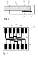
- FIG. 1 schematically shows a side view of a sensor architecture for screening of drugs-of-abuse comprising an electronic analyzer 10 which can process a sample provided in a disposable IVD cartridge 100.
- the electronic analyzer 10 comprises a PCB board 12 with a sensor driver, a controller etc. that carries a sensor interface 11. All components of the electronic analyzer 10 are reusable.
- the whole IVD cartridge 100 is disposable. It comprises a first plastic component 110 with micro fluidic cavities (not shown) and a disposable sensor located in a second plastic component 120.
- the sensor architecture of Figure 1 realizes a split of a micro-electronic sensor into a disposable part 100 and a reusable part 10.
- Many in-vitro diagnostic products consist of an electronic analyzer in combination with disposable cartridges and are therefore apt for such a split design.
- the manufacturing of a disposable micro fluidic device with electrical components will in the following be described with respect to an exemplary micro flow sensor.
- the flow sensor is based on the principle of providing heat using a centrally placed (resistive) heating element and measuring the difference in temperature on both sides of the heater resulting from convective heat transport by a fluid.
- Figure 2 shows a top view onto a plastic component 122 (referred to as "second plastic component” in this application) with a structured metal layer 121 on top.
- the metal layer 121 comprises a centrally placed resistive heater 123 with temperature sensing elements 124 on both sides. Temperature sensing in the heat sensors 124 is based on variation in electrical resistance due to variation in temperature.
- Figure 3 shows a top view onto the aforementioned second plastic component 122 with the structured metal layer 121 after it has been joined with a "first plastic component" 110 comprising microfluidic cavities, particularly a flow channel 111.
- first plastic component 110 comprising microfluidic cavities, particularly a flow channel 111.
- the micro electrical circuit of the flow sensor is realized in a single metal layer 121 on a plastic substrate 122. Therefore, heating and sensing elements are all made from the same metal, e.g. gold (Au). Initially, the gold is a continuous layer on the plastic substrate 122. This layer can be applied to the substrate either by sputtering, electrochemical plating, (screen) printing, or vapor deposition techniques. The actual layout of the flow sensor is realized by "isolating" the electrical circuit from its surroundings via laser ablation.
- Figures 4 and 5 show the result of the aforementioned procedure when the flow sensor is realized in a 30 nm gold layer 121 on a 20 micron thick PET plastic foil.
- This microfluidic device 200 comprises a 20 ⁇ m PET foil 222 ("second plastic component") with a laser-structured 30 nm Au layer 221 on top that constitutes a flow sensor.
- the foil 222 is stretched over a hole, cut out of a printed circuit board (PCB) 250 to monitor the thermal fluidic behavior of the sensor with an IR camera (not shown).
- the electrical connections from the PCB 250 to the metal layer 221 are made using electrically conducting wires that were soldered to the PCB 250 and connected using an electrically conducting adhesive to the Au layer 221.
- the foil 222 is joined with a plastic transparent substrate 213 providing the fluidic interconnection 214 using a patterned double-sided tape 212 to define the dimensions of the fluidic channel 211.
- the described thermal flow sensor is located at the side-wall of the channel 211 and is used for liquid flow sensing.
- Figures 7 and 8 show the resistance R as a function of time t for a flow rate of 2.5 ⁇ L/min, wherein letters "A" indicate times during which flow was "on", while letters "B" indicate times during which flow was “off”.
- the sensing element at the downstream location ( Figure 7 ) displays an increase in resistance in case liquid flow is applied (A). This is the result of increase in temperature due to convective heat transport from the heater located upstream. Contrary, the sensing element located upstream of the heater ( Figure 8 ) displays a decrease in resistance during flow (A) due to cooling.
- the enlarged diagram of Figure 10 shows that the flow sensor has a linear operating mode for flow rates up to about 15 ⁇ L/min.
- the present invention focuses on system architecture of sensors by splitting the physical embodiment of a sensor into a re-usable and a disposable part. It proposes the creation of the low cost disposable part of micro electronic sensors and actuators for use in plastic micro fluidic devices by structuring a thin and (initially) continuous or coarsely defined metal layer on a plastic substrate using laser ablation.
- the metal layer can be applied on a plastic substrate using sputtering, (screen) printing, electrochemical plating, or vapor deposition.
- the metal layer is initially a continuous layer or a metal layer with a coarsely defined outer contour.
- a structured micro-electronic circuit can be electrically isolated from its surroundings and/or final electrical layout can be fine tuned.
- the plastic substrate can be an injection molded part with a microstructured surface displaying a micro fluidic circuit. In this way the sensor or actuator is integrated with the microfluidic circuit and is created in-situ. Another possibility is to create the sensor or actuator on a thin plastic flexible foil.
- the plastic foil could be glued or thermally welded onto a plastic counter part, in this way creating a closed microfluidic channel.
- the flexible foil with micro-electronic circuit could be bend to follow the inner/outer contours of a (microfluidic) device or the inner diameter of a device used in minimally invasive surgery such as a catheter or endoscope.
- the materials and the production methods used to realize the micro-electronic sensors and actuators result in significant advantages for use in (disposable) plastic microfluidic devices.
- a micro flow sensor with overall dimensions in the order of several square millimeters has been realized on a thin plastic substrate, i.e. on a 20 micron thick PET foil.
- microfluidic channels can be part of larger devices with use in various applications:
Landscapes
- Chemical & Material Sciences (AREA)
- Engineering & Computer Science (AREA)
- Dispersion Chemistry (AREA)
- Health & Medical Sciences (AREA)
- Analytical Chemistry (AREA)
- Manufacturing & Machinery (AREA)
- General Health & Medical Sciences (AREA)
- Hematology (AREA)
- Clinical Laboratory Science (AREA)
- Chemical Kinetics & Catalysis (AREA)
- Microelectronics & Electronic Packaging (AREA)
- Micromachines (AREA)
Priority Applications (2)
| Application Number | Priority Date | Filing Date | Title |
|---|---|---|---|
| EP10196094A EP2468403A1 (fr) | 2010-12-21 | 2010-12-21 | Procédé pour la fabrication d'un dispositif microfluidique |
| PCT/IB2011/055568 WO2012085737A1 (fr) | 2010-12-21 | 2011-12-09 | Procédé de fabrication d'un dispositif microfluidique |
Applications Claiming Priority (1)
| Application Number | Priority Date | Filing Date | Title |
|---|---|---|---|
| EP10196094A EP2468403A1 (fr) | 2010-12-21 | 2010-12-21 | Procédé pour la fabrication d'un dispositif microfluidique |
Publications (1)
| Publication Number | Publication Date |
|---|---|
| EP2468403A1 true EP2468403A1 (fr) | 2012-06-27 |
Family
ID=43708886
Family Applications (1)
| Application Number | Title | Priority Date | Filing Date |
|---|---|---|---|
| EP10196094A Ceased EP2468403A1 (fr) | 2010-12-21 | 2010-12-21 | Procédé pour la fabrication d'un dispositif microfluidique |
Country Status (2)
| Country | Link |
|---|---|
| EP (1) | EP2468403A1 (fr) |
| WO (1) | WO2012085737A1 (fr) |
Cited By (5)
| Publication number | Priority date | Publication date | Assignee | Title |
|---|---|---|---|---|
| CN103011055A (zh) * | 2012-11-28 | 2013-04-03 | 苏州大学 | 一种微颗粒生产设备及生产方法 |
| CN104708800A (zh) * | 2013-12-11 | 2015-06-17 | 中国科学院深圳先进技术研究院 | 制作环烯烃类聚合物微流控芯片中微纳结构的软压印方法 |
| EP3164684A4 (fr) * | 2014-07-02 | 2018-01-10 | Canon U.S. Life Sciences, Inc. | Procédé pour produire un canal microfluidique enfoui doté d'élément chauffant intégré |
| CN109317228A (zh) * | 2018-11-01 | 2019-02-12 | 北京工业大学 | 一种基于激光内雕微加工的微流控芯片制备方法 |
| EP3912722A1 (fr) * | 2020-05-21 | 2021-11-24 | Biothink Technologies S.L. | Laboratoire intégré sur une puce et procédure de fabrication |
Families Citing this family (1)
| Publication number | Priority date | Publication date | Assignee | Title |
|---|---|---|---|---|
| CN110713168B (zh) * | 2018-07-13 | 2023-09-26 | 浙江清华柔性电子技术研究院 | 微流体器件的制备方法 |
Citations (8)
| Publication number | Priority date | Publication date | Assignee | Title |
|---|---|---|---|---|
| WO2000077509A1 (fr) * | 1999-06-16 | 2000-12-21 | Merck Patent Gmbh | Systeme d'analyse miniaturise |
| US20020122747A1 (en) * | 2000-09-19 | 2002-09-05 | Mingqi Zhao | Integrated microdevices for conducting chemical operations |
| EP1362827A1 (fr) * | 2002-05-16 | 2003-11-19 | Micronit Microfluidics B.V. | Méthode de fabrication d'un dispositif microfluidique |
| US20050130292A1 (en) | 2003-09-26 | 2005-06-16 | The University Of Cincinnati | Smart disposable plastic lab-on-a-chip for point-of-care testing |
| WO2005119200A1 (fr) * | 2004-06-01 | 2005-12-15 | Epocal Inc. | Dispositifs de diagnostic intégrant des éléments fluidiques et procédés de fabrication |
| WO2007029133A2 (fr) * | 2005-09-09 | 2007-03-15 | Koninklijke Philips Electronics N. V. | Procede de fabrication de microsysteme, microsysteme, empilement de feuilles comprenant ce microsysteme, dispositif electronique comprenant ce microsysteme et utilisation de ce dispositif electronique |
| WO2007085043A1 (fr) * | 2006-01-24 | 2007-08-02 | Mycrolab Pty Ltd | Procédés de fabrication bon marché de matériaux et dispositifs stratifiés complexes |
| US20080233011A1 (en) * | 2007-03-23 | 2008-09-25 | 3M Innovative Properties Company | Microfluidic devices |
-
2010
- 2010-12-21 EP EP10196094A patent/EP2468403A1/fr not_active Ceased
-
2011
- 2011-12-09 WO PCT/IB2011/055568 patent/WO2012085737A1/fr not_active Ceased
Patent Citations (8)
| Publication number | Priority date | Publication date | Assignee | Title |
|---|---|---|---|---|
| WO2000077509A1 (fr) * | 1999-06-16 | 2000-12-21 | Merck Patent Gmbh | Systeme d'analyse miniaturise |
| US20020122747A1 (en) * | 2000-09-19 | 2002-09-05 | Mingqi Zhao | Integrated microdevices for conducting chemical operations |
| EP1362827A1 (fr) * | 2002-05-16 | 2003-11-19 | Micronit Microfluidics B.V. | Méthode de fabrication d'un dispositif microfluidique |
| US20050130292A1 (en) | 2003-09-26 | 2005-06-16 | The University Of Cincinnati | Smart disposable plastic lab-on-a-chip for point-of-care testing |
| WO2005119200A1 (fr) * | 2004-06-01 | 2005-12-15 | Epocal Inc. | Dispositifs de diagnostic intégrant des éléments fluidiques et procédés de fabrication |
| WO2007029133A2 (fr) * | 2005-09-09 | 2007-03-15 | Koninklijke Philips Electronics N. V. | Procede de fabrication de microsysteme, microsysteme, empilement de feuilles comprenant ce microsysteme, dispositif electronique comprenant ce microsysteme et utilisation de ce dispositif electronique |
| WO2007085043A1 (fr) * | 2006-01-24 | 2007-08-02 | Mycrolab Pty Ltd | Procédés de fabrication bon marché de matériaux et dispositifs stratifiés complexes |
| US20080233011A1 (en) * | 2007-03-23 | 2008-09-25 | 3M Innovative Properties Company | Microfluidic devices |
Cited By (11)
| Publication number | Priority date | Publication date | Assignee | Title |
|---|---|---|---|---|
| CN103011055A (zh) * | 2012-11-28 | 2013-04-03 | 苏州大学 | 一种微颗粒生产设备及生产方法 |
| CN103011055B (zh) * | 2012-11-28 | 2015-07-15 | 苏州大学 | 一种微颗粒生产设备及生产方法 |
| CN104708800A (zh) * | 2013-12-11 | 2015-06-17 | 中国科学院深圳先进技术研究院 | 制作环烯烃类聚合物微流控芯片中微纳结构的软压印方法 |
| EP3164684A4 (fr) * | 2014-07-02 | 2018-01-10 | Canon U.S. Life Sciences, Inc. | Procédé pour produire un canal microfluidique enfoui doté d'élément chauffant intégré |
| CN109317228A (zh) * | 2018-11-01 | 2019-02-12 | 北京工业大学 | 一种基于激光内雕微加工的微流控芯片制备方法 |
| CN109317228B (zh) * | 2018-11-01 | 2021-02-26 | 北京工业大学 | 一种基于激光内雕微加工的微流控芯片制备方法 |
| EP3912722A1 (fr) * | 2020-05-21 | 2021-11-24 | Biothink Technologies S.L. | Laboratoire intégré sur une puce et procédure de fabrication |
| WO2021233814A1 (fr) * | 2020-05-21 | 2021-11-25 | Biothink Technologies, S.L. | Procédé de fabrication de laboratoire intégré sur une puce |
| CN115885589A (zh) * | 2020-05-21 | 2023-03-31 | 生物思维科技有限公司 | 集成在芯片上的实验室的制造过程 |
| JP2023527790A (ja) * | 2020-05-21 | 2023-06-30 | バイオシンク・テクノロジーズ・ソシエダッド・リミターダ | チップ上に統合されたラボラトリの製造方法 |
| CN115885589B (zh) * | 2020-05-21 | 2026-04-17 | 生物思维科技有限公司 | 集成在芯片上的实验室的制造过程 |
Also Published As
| Publication number | Publication date |
|---|---|
| WO2012085737A1 (fr) | 2012-06-28 |
Similar Documents
| Publication | Publication Date | Title |
|---|---|---|
| Fallahi et al. | Flexible microfluidics: Fundamentals, recent developments, and applications | |
| WO2012085737A1 (fr) | Procédé de fabrication d'un dispositif microfluidique | |
| Kamat et al. | Biomimetic soft polymer microstructures and piezoresistive graphene MEMS sensors using sacrificial metal 3D printing | |
| JP5579443B2 (ja) | マイクロ流体デバイス | |
| Papamatthaiou et al. | Recent advances in bio-microsystem integration and Lab-on-PCB technology | |
| WO2007064117A1 (fr) | Microdispositif de chromatographie par affinite et procede de fabrication correspondant | |
| US7652370B2 (en) | Plastic microfabricated structure for biochip, microfabricated thermal device, microfabricated reactor, microfabricated reactor array, and micro array using the same | |
| Mohammadzadeh et al. | Rapid and inexpensive method for fabrication and integration of electrodes in microfluidic devices | |
| WO2012085728A1 (fr) | Dispositif microfluidique comprenant un moyen de commande du flux de fluide | |
| Heckele et al. | Replication and bonding techniques for integrated microfluidic systems | |
| He et al. | Automating fluid delivery in a capillary microfluidic device using low-voltage electrowetting valves | |
| Farooq et al. | Thin flexible lab-on-a-film for impedimetric sensing in biomedical applications | |
| Attia et al. | Integration of functionality into polymer-based microfluidic devices produced by high-volume micro-moulding techniques | |
| JP6240615B2 (ja) | 流体を処理するカートリッジ | |
| Zhao et al. | Heavily-doped bulk silicon sidewall electrodes embedded between free-hanging microfluidic channels by modified surface channel technology | |
| Salvador et al. | Fabrication process for inexpensive, biocompatible and transparent PCBs. Application to a flow meter | |
| EP4153353B1 (fr) | Procédure de fabrication pour un laboratoire intégré sur une puce | |
| Boustheen et al. | A layered modular polymeric μ-valve suitable for lab-on-foil: design, fabrication, and characterization | |
| KR100779083B1 (ko) | 플라스틱 미세가열 시스템, 그 미세가열 시스템을 이용한랩온어칩, 및 그 미세가열 시스템의 제조방법 | |
| JP2006300145A (ja) | マイクロバルブ及び該マイクロバルブを有するマイクロチップ | |
| Toh et al. | Modular membrane valves for universal integration within thermoplastic devices | |
| Gray | Bio-microinstrumentation technology: discrete components to modular systems | |
| KR20060065456A (ko) | 플라스틱 기판을 이용한 미소 가열기 및 그의 제조 방법 | |
| HK40090522A (en) | Manufacturing procedure for laboratory integrated on a chip | |
| HK40090522B (en) | Manufacturing procedure for laboratory integrated on a chip |
Legal Events
| Date | Code | Title | Description |
|---|---|---|---|
| AK | Designated contracting states |
Kind code of ref document: A1 Designated state(s): AL AT BE BG CH CY CZ DE DK EE ES FI FR GB GR HR HU IE IS IT LI LT LU LV MC MK MT NL NO PL PT RO RS SE SI SK SM TR |
|
| AX | Request for extension of the european patent |
Extension state: BA ME |
|
| PUAI | Public reference made under article 153(3) epc to a published international application that has entered the european phase |
Free format text: ORIGINAL CODE: 0009012 |
|
| STAA | Information on the status of an ep patent application or granted ep patent |
Free format text: STATUS: THE APPLICATION HAS BEEN REFUSED |
|
| 18R | Application refused |
Effective date: 20120721 |