EP2469598A2 - Sensorchip, Erfassungsvorrichtung und Verfahren zur Herstellung eines Sensorchips - Google Patents
Sensorchip, Erfassungsvorrichtung und Verfahren zur Herstellung eines Sensorchips Download PDFInfo
- Publication number
- EP2469598A2 EP2469598A2 EP20110195171 EP11195171A EP2469598A2 EP 2469598 A2 EP2469598 A2 EP 2469598A2 EP 20110195171 EP20110195171 EP 20110195171 EP 11195171 A EP11195171 A EP 11195171A EP 2469598 A2 EP2469598 A2 EP 2469598A2
- Authority
- EP
- European Patent Office
- Prior art keywords
- sensor chip
- metal particles
- fine metal
- relief structure
- substrate
- Prior art date
- Legal status (The legal status is an assumption and is not a legal conclusion. Google has not performed a legal analysis and makes no representation as to the accuracy of the status listed.)
- Withdrawn
Links
- 238000001514 detection method Methods 0.000 title claims description 61
- 238000004519 manufacturing process Methods 0.000 title claims description 20
- 239000002923 metal particle Substances 0.000 claims abstract description 129
- 229910001111 Fine metal Inorganic materials 0.000 claims abstract description 128
- 239000000758 substrate Substances 0.000 claims abstract description 52
- 238000002198 surface plasmon resonance spectroscopy Methods 0.000 claims abstract description 37
- 238000004416 surface enhanced Raman spectroscopy Methods 0.000 claims abstract description 21
- 238000000034 method Methods 0.000 claims description 47
- 239000007788 liquid Substances 0.000 claims description 33
- 239000006185 dispersion Substances 0.000 claims description 31
- 239000002612 dispersion medium Substances 0.000 claims description 29
- 230000005684 electric field Effects 0.000 claims description 29
- 239000013076 target substance Substances 0.000 claims description 28
- 238000001069 Raman spectroscopy Methods 0.000 claims description 26
- 230000008569 process Effects 0.000 claims description 22
- 239000002245 particle Substances 0.000 claims description 18
- KDLHZDBZIXYQEI-UHFFFAOYSA-N Palladium Chemical compound [Pd] KDLHZDBZIXYQEI-UHFFFAOYSA-N 0.000 claims description 13
- BASFCYQUMIYNBI-UHFFFAOYSA-N platinum Chemical compound [Pt] BASFCYQUMIYNBI-UHFFFAOYSA-N 0.000 claims description 13
- 229910052709 silver Inorganic materials 0.000 claims description 13
- 239000010931 gold Substances 0.000 claims description 12
- BQCADISMDOOEFD-UHFFFAOYSA-N Silver Chemical compound [Ag] BQCADISMDOOEFD-UHFFFAOYSA-N 0.000 claims description 11
- 239000011651 chromium Substances 0.000 claims description 9
- 239000010949 copper Substances 0.000 claims description 9
- 238000012545 processing Methods 0.000 claims description 9
- 239000004332 silver Substances 0.000 claims description 9
- 229910052737 gold Inorganic materials 0.000 claims description 8
- 230000003287 optical effect Effects 0.000 claims description 8
- 239000003989 dielectric material Substances 0.000 claims description 6
- 229910052751 metal Inorganic materials 0.000 claims description 6
- 239000002184 metal Substances 0.000 claims description 6
- 229910052804 chromium Inorganic materials 0.000 claims description 5
- 229910052802 copper Inorganic materials 0.000 claims description 5
- 229910052763 palladium Inorganic materials 0.000 claims description 5
- 229910052697 platinum Inorganic materials 0.000 claims description 5
- VYZAMTAEIAYCRO-UHFFFAOYSA-N Chromium Chemical compound [Cr] VYZAMTAEIAYCRO-UHFFFAOYSA-N 0.000 claims description 4
- RYGMFSIKBFXOCR-UHFFFAOYSA-N Copper Chemical compound [Cu] RYGMFSIKBFXOCR-UHFFFAOYSA-N 0.000 claims description 4
- ZOKXTWBITQBERF-UHFFFAOYSA-N Molybdenum Chemical compound [Mo] ZOKXTWBITQBERF-UHFFFAOYSA-N 0.000 claims description 4
- 229910045601 alloy Inorganic materials 0.000 claims description 4
- 239000000956 alloy Substances 0.000 claims description 4
- 229910052782 aluminium Inorganic materials 0.000 claims description 4
- XAGFODPZIPBFFR-UHFFFAOYSA-N aluminium Chemical compound [Al] XAGFODPZIPBFFR-UHFFFAOYSA-N 0.000 claims description 4
- PCHJSUWPFVWCPO-UHFFFAOYSA-N gold Chemical compound [Au] PCHJSUWPFVWCPO-UHFFFAOYSA-N 0.000 claims description 4
- 150000002739 metals Chemical class 0.000 claims description 4
- 229910052750 molybdenum Inorganic materials 0.000 claims description 4
- 239000011733 molybdenum Substances 0.000 claims description 4
- 230000001678 irradiating effect Effects 0.000 abstract description 14
- 230000035945 sensitivity Effects 0.000 abstract description 14
- 239000000126 substance Substances 0.000 abstract description 12
- 238000010586 diagram Methods 0.000 description 21
- 238000001228 spectrum Methods 0.000 description 13
- 239000000463 material Substances 0.000 description 12
- SQGYOTSLMSWVJD-UHFFFAOYSA-N silver(1+) nitrate Chemical compound [Ag+].[O-]N(=O)=O SQGYOTSLMSWVJD-UHFFFAOYSA-N 0.000 description 12
- 239000000243 solution Substances 0.000 description 9
- 238000001704 evaporation Methods 0.000 description 8
- 239000010453 quartz Substances 0.000 description 7
- VYPSYNLAJGMNEJ-UHFFFAOYSA-N silicon dioxide Inorganic materials O=[Si]=O VYPSYNLAJGMNEJ-UHFFFAOYSA-N 0.000 description 7
- IKHGUXGNUITLKF-UHFFFAOYSA-N Acetaldehyde Chemical group CC=O IKHGUXGNUITLKF-UHFFFAOYSA-N 0.000 description 6
- CSCPPACGZOOCGX-UHFFFAOYSA-N Acetone Chemical compound CC(C)=O CSCPPACGZOOCGX-UHFFFAOYSA-N 0.000 description 6
- UHOVQNZJYSORNB-UHFFFAOYSA-N Benzene Chemical compound C1=CC=CC=C1 UHOVQNZJYSORNB-UHFFFAOYSA-N 0.000 description 6
- FOIXSVOLVBLSDH-UHFFFAOYSA-N Silver ion Chemical compound [Ag+] FOIXSVOLVBLSDH-UHFFFAOYSA-N 0.000 description 6
- YXFVVABEGXRONW-UHFFFAOYSA-N Toluene Chemical compound CC1=CC=CC=C1 YXFVVABEGXRONW-UHFFFAOYSA-N 0.000 description 6
- 230000009471 action Effects 0.000 description 6
- 230000008020 evaporation Effects 0.000 description 6
- 239000003574 free electron Substances 0.000 description 6
- 229910001961 silver nitrate Inorganic materials 0.000 description 6
- -1 alkyl naphthalene Chemical compound 0.000 description 5
- 239000007789 gas Substances 0.000 description 5
- 238000005530 etching Methods 0.000 description 4
- 229910000358 iron sulfate Inorganic materials 0.000 description 4
- BAUYGSIQEAFULO-UHFFFAOYSA-L iron(2+) sulfate (anhydrous) Chemical compound [Fe+2].[O-]S([O-])(=O)=O BAUYGSIQEAFULO-UHFFFAOYSA-L 0.000 description 4
- 238000005259 measurement Methods 0.000 description 4
- 239000002609 medium Substances 0.000 description 4
- NLJMYIDDQXHKNR-UHFFFAOYSA-K sodium citrate Chemical compound O.O.[Na+].[Na+].[Na+].[O-]C(=O)CC(O)(CC([O-])=O)C([O-])=O NLJMYIDDQXHKNR-UHFFFAOYSA-K 0.000 description 4
- 239000001509 sodium citrate Substances 0.000 description 4
- 239000012855 volatile organic compound Substances 0.000 description 4
- ZWEHNKRNPOVVGH-UHFFFAOYSA-N 2-Butanone Chemical compound CCC(C)=O ZWEHNKRNPOVVGH-UHFFFAOYSA-N 0.000 description 3
- WEVYAHXRMPXWCK-UHFFFAOYSA-N Acetonitrile Chemical compound CC#N WEVYAHXRMPXWCK-UHFFFAOYSA-N 0.000 description 3
- YMWUJEATGCHHMB-UHFFFAOYSA-N Dichloromethane Chemical compound ClCCl YMWUJEATGCHHMB-UHFFFAOYSA-N 0.000 description 3
- QMMFVYPAHWMCMS-UHFFFAOYSA-N Dimethyl sulfide Chemical compound CSC QMMFVYPAHWMCMS-UHFFFAOYSA-N 0.000 description 3
- LFQSCWFLJHTTHZ-UHFFFAOYSA-N Ethanol Chemical compound CCO LFQSCWFLJHTTHZ-UHFFFAOYSA-N 0.000 description 3
- XEKOWRVHYACXOJ-UHFFFAOYSA-N Ethyl acetate Chemical compound CCOC(C)=O XEKOWRVHYACXOJ-UHFFFAOYSA-N 0.000 description 3
- LYCAIKOWRPUZTN-UHFFFAOYSA-N Ethylene glycol Chemical compound OCCO LYCAIKOWRPUZTN-UHFFFAOYSA-N 0.000 description 3
- OKKJLVBELUTLKV-UHFFFAOYSA-N Methanol Chemical compound OC OKKJLVBELUTLKV-UHFFFAOYSA-N 0.000 description 3
- ZMXDDKWLCZADIW-UHFFFAOYSA-N N,N-Dimethylformamide Chemical compound CN(C)C=O ZMXDDKWLCZADIW-UHFFFAOYSA-N 0.000 description 3
- 238000007605 air drying Methods 0.000 description 3
- 230000008901 benefit Effects 0.000 description 3
- 238000009835 boiling Methods 0.000 description 3
- 239000005388 borosilicate glass Substances 0.000 description 3
- 239000013078 crystal Substances 0.000 description 3
- MTHSVFCYNBDYFN-UHFFFAOYSA-N diethylene glycol Chemical compound OCCOCCO MTHSVFCYNBDYFN-UHFFFAOYSA-N 0.000 description 3
- 239000000428 dust Substances 0.000 description 3
- 239000011521 glass Substances 0.000 description 3
- 239000000203 mixture Substances 0.000 description 3
- VLKZOEOYAKHREP-UHFFFAOYSA-N n-Hexane Chemical compound CCCCCC VLKZOEOYAKHREP-UHFFFAOYSA-N 0.000 description 3
- 230000000149 penetrating effect Effects 0.000 description 3
- 238000002360 preparation method Methods 0.000 description 3
- 229910052710 silicon Inorganic materials 0.000 description 3
- 239000010703 silicon Substances 0.000 description 3
- KBPLFHHGFOOTCA-UHFFFAOYSA-N 1-Octanol Chemical compound CCCCCCCCO KBPLFHHGFOOTCA-UHFFFAOYSA-N 0.000 description 2
- SYBYTAAJFKOIEJ-UHFFFAOYSA-N 3-Methylbutan-2-one Chemical compound CC(C)C(C)=O SYBYTAAJFKOIEJ-UHFFFAOYSA-N 0.000 description 2
- HEDRZPFGACZZDS-UHFFFAOYSA-N Chloroform Chemical compound ClC(Cl)Cl HEDRZPFGACZZDS-UHFFFAOYSA-N 0.000 description 2
- YNQLUTRBYVCPMQ-UHFFFAOYSA-N Ethylbenzene Chemical compound CCC1=CC=CC=C1 YNQLUTRBYVCPMQ-UHFFFAOYSA-N 0.000 description 2
- YLQBMQCUIZJEEH-UHFFFAOYSA-N Furan Chemical compound C=1C=COC=1 YLQBMQCUIZJEEH-UHFFFAOYSA-N 0.000 description 2
- PEDCQBHIVMGVHV-UHFFFAOYSA-N Glycerine Chemical compound OCC(O)CO PEDCQBHIVMGVHV-UHFFFAOYSA-N 0.000 description 2
- LTEQMZWBSYACLV-UHFFFAOYSA-N Hexylbenzene Chemical compound CCCCCCC1=CC=CC=C1 LTEQMZWBSYACLV-UHFFFAOYSA-N 0.000 description 2
- RRHGJUQNOFWUDK-UHFFFAOYSA-N Isoprene Chemical compound CC(=C)C=C RRHGJUQNOFWUDK-UHFFFAOYSA-N 0.000 description 2
- KFZMGEQAYNKOFK-UHFFFAOYSA-N Isopropanol Chemical compound CC(C)O KFZMGEQAYNKOFK-UHFFFAOYSA-N 0.000 description 2
- LSDPWZHWYPCBBB-UHFFFAOYSA-N Methanethiol Chemical compound SC LSDPWZHWYPCBBB-UHFFFAOYSA-N 0.000 description 2
- LRHPLDYGYMQRHN-UHFFFAOYSA-N N-Butanol Chemical compound CCCCO LRHPLDYGYMQRHN-UHFFFAOYSA-N 0.000 description 2
- OFBQJSOFQDEBGM-UHFFFAOYSA-N Pentane Chemical compound CCCCC OFBQJSOFQDEBGM-UHFFFAOYSA-N 0.000 description 2
- XBDQKXXYIPTUBI-UHFFFAOYSA-M Propionate Chemical compound CCC([O-])=O XBDQKXXYIPTUBI-UHFFFAOYSA-M 0.000 description 2
- KYQCOXFCLRTKLS-UHFFFAOYSA-N Pyrazine Chemical compound C1=CN=CC=N1 KYQCOXFCLRTKLS-UHFFFAOYSA-N 0.000 description 2
- JUJWROOIHBZHMG-UHFFFAOYSA-N Pyridine Chemical compound C1=CC=NC=C1 JUJWROOIHBZHMG-UHFFFAOYSA-N 0.000 description 2
- KAESVJOAVNADME-UHFFFAOYSA-N Pyrrole Chemical compound C=1C=CNC=1 KAESVJOAVNADME-UHFFFAOYSA-N 0.000 description 2
- PPBRXRYQALVLMV-UHFFFAOYSA-N Styrene Chemical compound C=CC1=CC=CC=C1 PPBRXRYQALVLMV-UHFFFAOYSA-N 0.000 description 2
- YTPLMLYBLZKORZ-UHFFFAOYSA-N Thiophene Chemical compound C=1C=CSC=1 YTPLMLYBLZKORZ-UHFFFAOYSA-N 0.000 description 2
- IKHGUXGNUITLKF-XPULMUKRSA-N acetaldehyde Chemical group [14CH]([14CH3])=O IKHGUXGNUITLKF-XPULMUKRSA-N 0.000 description 2
- OCKPCBLVNKHBMX-UHFFFAOYSA-N butylbenzene Chemical compound CCCCC1=CC=CC=C1 OCKPCBLVNKHBMX-UHFFFAOYSA-N 0.000 description 2
- HVYWMOMLDIMFJA-DPAQBDIFSA-N cholesterol Chemical compound C1C=C2C[C@@H](O)CC[C@]2(C)[C@@H]2[C@@H]1[C@@H]1CC[C@H]([C@H](C)CCCC(C)C)[C@@]1(C)CC2 HVYWMOMLDIMFJA-DPAQBDIFSA-N 0.000 description 2
- 239000000470 constituent Substances 0.000 description 2
- 230000007423 decrease Effects 0.000 description 2
- UZILCZKGXMQEQR-UHFFFAOYSA-N decyl-Benzene Chemical compound CCCCCCCCCCC1=CC=CC=C1 UZILCZKGXMQEQR-UHFFFAOYSA-N 0.000 description 2
- 238000001035 drying Methods 0.000 description 2
- 238000010894 electron beam technology Methods 0.000 description 2
- 238000005516 engineering process Methods 0.000 description 2
- 239000012530 fluid Substances 0.000 description 2
- 238000012388 gravitational sedimentation Methods 0.000 description 2
- 230000005484 gravity Effects 0.000 description 2
- 229930195733 hydrocarbon Natural products 0.000 description 2
- 230000006872 improvement Effects 0.000 description 2
- 230000001965 increasing effect Effects 0.000 description 2
- 238000007689 inspection Methods 0.000 description 2
- 239000002082 metal nanoparticle Substances 0.000 description 2
- UAEPNZWRGJTJPN-UHFFFAOYSA-N methylcyclohexane Chemical compound CC1CCCCC1 UAEPNZWRGJTJPN-UHFFFAOYSA-N 0.000 description 2
- FDPIMTJIUBPUKL-UHFFFAOYSA-N pentan-3-one Chemical compound CCC(=O)CC FDPIMTJIUBPUKL-UHFFFAOYSA-N 0.000 description 2
- 238000001179 sorption measurement Methods 0.000 description 2
- 238000003892 spreading Methods 0.000 description 2
- 230000007480 spreading Effects 0.000 description 2
- VZGDMQKNWNREIO-UHFFFAOYSA-N tetrachloromethane Chemical compound ClC(Cl)(Cl)Cl VZGDMQKNWNREIO-UHFFFAOYSA-N 0.000 description 2
- MCVUKOYZUCWLQQ-UHFFFAOYSA-N tridecylbenzene Chemical compound CCCCCCCCCCCCCC1=CC=CC=C1 MCVUKOYZUCWLQQ-UHFFFAOYSA-N 0.000 description 2
- 239000002699 waste material Substances 0.000 description 2
- WSLDOOZREJYCGB-UHFFFAOYSA-N 1,2-Dichloroethane Chemical compound ClCCCl WSLDOOZREJYCGB-UHFFFAOYSA-N 0.000 description 1
- XNWFRZJHXBZDAG-UHFFFAOYSA-N 2-METHOXYETHANOL Chemical compound COCCO XNWFRZJHXBZDAG-UHFFFAOYSA-N 0.000 description 1
- ZNQVEEAIQZEUHB-UHFFFAOYSA-N 2-ethoxyethanol Chemical compound CCOCCO ZNQVEEAIQZEUHB-UHFFFAOYSA-N 0.000 description 1
- QCDWFXQBSFUVSP-UHFFFAOYSA-N 2-phenoxyethanol Chemical compound OCCOC1=CC=CC=C1 QCDWFXQBSFUVSP-UHFFFAOYSA-N 0.000 description 1
- NLHHRLWOUZZQLW-UHFFFAOYSA-N Acrylonitrile Chemical compound C=CC#N NLHHRLWOUZZQLW-UHFFFAOYSA-N 0.000 description 1
- DKPFZGUDAPQIHT-UHFFFAOYSA-N Butyl acetate Natural products CCCCOC(C)=O DKPFZGUDAPQIHT-UHFFFAOYSA-N 0.000 description 1
- UGFAIRIUMAVXCW-UHFFFAOYSA-N Carbon monoxide Chemical compound [O+]#[C-] UGFAIRIUMAVXCW-UHFFFAOYSA-N 0.000 description 1
- 208000035473 Communicable disease Diseases 0.000 description 1
- XDTMQSROBMDMFD-UHFFFAOYSA-N Cyclohexane Chemical compound C1CCCCC1 XDTMQSROBMDMFD-UHFFFAOYSA-N 0.000 description 1
- RWSOTUBLDIXVET-UHFFFAOYSA-N Dihydrogen sulfide Chemical compound S RWSOTUBLDIXVET-UHFFFAOYSA-N 0.000 description 1
- NTIZESTWPVYFNL-UHFFFAOYSA-N Methyl isobutyl ketone Chemical compound CC(C)CC(C)=O NTIZESTWPVYFNL-UHFFFAOYSA-N 0.000 description 1
- UIHCLUNTQKBZGK-UHFFFAOYSA-N Methyl isobutyl ketone Natural products CCC(C)C(C)=O UIHCLUNTQKBZGK-UHFFFAOYSA-N 0.000 description 1
- FXHOOIRPVKKKFG-UHFFFAOYSA-N N,N-Dimethylacetamide Chemical compound CN(C)C(C)=O FXHOOIRPVKKKFG-UHFFFAOYSA-N 0.000 description 1
- SECXISVLQFMRJM-UHFFFAOYSA-N N-Methylpyrrolidone Chemical compound CN1CCCC1=O SECXISVLQFMRJM-UHFFFAOYSA-N 0.000 description 1
- 206010028980 Neoplasm Diseases 0.000 description 1
- CTQNGGLPUBDAKN-UHFFFAOYSA-N O-Xylene Chemical compound CC1=CC=CC=C1C CTQNGGLPUBDAKN-UHFFFAOYSA-N 0.000 description 1
- PCNDJXKNXGMECE-UHFFFAOYSA-N Phenazine Natural products C1=CC=CC2=NC3=CC=CC=C3N=C21 PCNDJXKNXGMECE-UHFFFAOYSA-N 0.000 description 1
- 241000700605 Viruses Species 0.000 description 1
- 229910009372 YVO4 Inorganic materials 0.000 description 1
- 238000002835 absorbance Methods 0.000 description 1
- 238000010521 absorption reaction Methods 0.000 description 1
- 238000000862 absorption spectrum Methods 0.000 description 1
- 238000009825 accumulation Methods 0.000 description 1
- KXKVLQRXCPHEJC-UHFFFAOYSA-N acetic acid trimethyl ester Natural products COC(C)=O KXKVLQRXCPHEJC-UHFFFAOYSA-N 0.000 description 1
- 150000001298 alcohols Chemical class 0.000 description 1
- 150000001338 aliphatic hydrocarbons Chemical class 0.000 description 1
- 150000004997 alkyl benzene derivatives Chemical class 0.000 description 1
- 125000000217 alkyl group Chemical group 0.000 description 1
- 150000001408 amides Chemical class 0.000 description 1
- 125000006615 aromatic heterocyclic group Chemical group 0.000 description 1
- 150000004945 aromatic hydrocarbons Chemical class 0.000 description 1
- 208000006673 asthma Diseases 0.000 description 1
- 238000010923 batch production Methods 0.000 description 1
- 239000011324 bead Substances 0.000 description 1
- 150000001555 benzenes Chemical class 0.000 description 1
- BJQHLKABXJIVAM-UHFFFAOYSA-N bis(2-ethylhexyl) phthalate Chemical compound CCCCC(CC)COC(=O)C1=CC=CC=C1C(=O)OCC(CC)CCCC BJQHLKABXJIVAM-UHFFFAOYSA-N 0.000 description 1
- 230000000903 blocking effect Effects 0.000 description 1
- 201000011510 cancer Diseases 0.000 description 1
- 238000006243 chemical reaction Methods 0.000 description 1
- 235000012000 cholesterol Nutrition 0.000 description 1
- 230000008602 contraction Effects 0.000 description 1
- 230000008878 coupling Effects 0.000 description 1
- 238000010168 coupling process Methods 0.000 description 1
- 238000005859 coupling reaction Methods 0.000 description 1
- JHIVVAPYMSGYDF-UHFFFAOYSA-N cyclohexanone Chemical compound O=C1CCCCC1 JHIVVAPYMSGYDF-UHFFFAOYSA-N 0.000 description 1
- 230000003247 decreasing effect Effects 0.000 description 1
- 230000008021 deposition Effects 0.000 description 1
- 238000011161 development Methods 0.000 description 1
- 238000007599 discharging Methods 0.000 description 1
- KWKXNDCHNDYVRT-UHFFFAOYSA-N dodecylbenzene Chemical compound CCCCCCCCCCCCC1=CC=CC=C1 KWKXNDCHNDYVRT-UHFFFAOYSA-N 0.000 description 1
- 239000003814 drug Substances 0.000 description 1
- 229940079593 drug Drugs 0.000 description 1
- 230000002708 enhancing effect Effects 0.000 description 1
- 150000002148 esters Chemical class 0.000 description 1
- 239000002360 explosive Substances 0.000 description 1
- 239000010419 fine particle Substances 0.000 description 1
- 235000013305 food Nutrition 0.000 description 1
- WBJINCZRORDGAQ-UHFFFAOYSA-N formic acid ethyl ester Natural products CCOC=O WBJINCZRORDGAQ-UHFFFAOYSA-N 0.000 description 1
- 235000011187 glycerol Nutrition 0.000 description 1
- 150000008282 halocarbons Chemical class 0.000 description 1
- 239000000383 hazardous chemical Substances 0.000 description 1
- 238000010438 heat treatment Methods 0.000 description 1
- FUZZWVXGSFPDMH-UHFFFAOYSA-M hexanoate Chemical compound CCCCCC([O-])=O FUZZWVXGSFPDMH-UHFFFAOYSA-M 0.000 description 1
- 150000002430 hydrocarbons Chemical class 0.000 description 1
- 229910000037 hydrogen sulfide Inorganic materials 0.000 description 1
- 230000001976 improved effect Effects 0.000 description 1
- 230000001939 inductive effect Effects 0.000 description 1
- 230000010354 integration Effects 0.000 description 1
- 150000002576 ketones Chemical class 0.000 description 1
- 230000008018 melting Effects 0.000 description 1
- 238000002844 melting Methods 0.000 description 1
- WSFSSNUMVMOOMR-NJFSPNSNSA-N methanone Chemical compound O=[14CH2] WSFSSNUMVMOOMR-NJFSPNSNSA-N 0.000 description 1
- GYNNXHKOJHMOHS-UHFFFAOYSA-N methyl-cycloheptane Natural products CC1CCCCCC1 GYNNXHKOJHMOHS-UHFFFAOYSA-N 0.000 description 1
- 239000011259 mixed solution Substances 0.000 description 1
- UFWIBTONFRDIAS-UHFFFAOYSA-N naphthalene-acid Natural products C1=CC=CC2=CC=CC=C21 UFWIBTONFRDIAS-UHFFFAOYSA-N 0.000 description 1
- 230000003533 narcotic effect Effects 0.000 description 1
- 150000002825 nitriles Chemical class 0.000 description 1
- LIXVMPBOGDCSRM-UHFFFAOYSA-N nonylbenzene Chemical compound CCCCCCCCCC1=CC=CC=C1 LIXVMPBOGDCSRM-UHFFFAOYSA-N 0.000 description 1
- TVMXDCGIABBOFY-UHFFFAOYSA-N octane Chemical compound CCCCCCCC TVMXDCGIABBOFY-UHFFFAOYSA-N 0.000 description 1
- VXNSQGRKHCZUSU-UHFFFAOYSA-N octylbenzene Chemical compound [CH2]CCCCCCCC1=CC=CC=C1 VXNSQGRKHCZUSU-UHFFFAOYSA-N 0.000 description 1
- 208000028169 periodontal disease Diseases 0.000 description 1
- 229920000768 polyamine Polymers 0.000 description 1
- 239000000843 powder Substances 0.000 description 1
- 230000001737 promoting effect Effects 0.000 description 1
- 230000001902 propagating effect Effects 0.000 description 1
- FVSKHRXBFJPNKK-UHFFFAOYSA-N propionitrile Chemical compound CCC#N FVSKHRXBFJPNKK-UHFFFAOYSA-N 0.000 description 1
- UMJSCPRVCHMLSP-UHFFFAOYSA-N pyridine Natural products COC1=CC=CN=C1 UMJSCPRVCHMLSP-UHFFFAOYSA-N 0.000 description 1
- 238000012216 screening Methods 0.000 description 1
- 238000007789 sealing Methods 0.000 description 1
- 238000000926 separation method Methods 0.000 description 1
- 239000010944 silver (metal) Substances 0.000 description 1
- 239000002356 single layer Substances 0.000 description 1
- 239000007787 solid Substances 0.000 description 1
- 230000003068 static effect Effects 0.000 description 1
- 239000004094 surface-active agent Substances 0.000 description 1
- 238000012360 testing method Methods 0.000 description 1
- JZALLXAUNPOCEU-UHFFFAOYSA-N tetradecylbenzene Chemical compound CCCCCCCCCCCCCCC1=CC=CC=C1 JZALLXAUNPOCEU-UHFFFAOYSA-N 0.000 description 1
- 229930192474 thiophene Natural products 0.000 description 1
- 239000011882 ultra-fine particle Substances 0.000 description 1
- XBEADGFTLHRJRB-UHFFFAOYSA-N undecylbenzene Chemical compound CCCCCCCCCCCC1=CC=CC=C1 XBEADGFTLHRJRB-UHFFFAOYSA-N 0.000 description 1
- 239000008096 xylene Substances 0.000 description 1
Images





Classifications
-
- G—PHYSICS
- G01—MEASURING; TESTING
- G01N—INVESTIGATING OR ANALYSING MATERIALS BY DETERMINING THEIR CHEMICAL OR PHYSICAL PROPERTIES
- G01N21/00—Investigating or analysing materials by the use of optical means, i.e. using sub-millimetre waves, infrared, visible or ultraviolet light
- G01N21/17—Systems in which incident light is modified in accordance with the properties of the material investigated
- G01N21/55—Specular reflectivity
- G01N21/552—Attenuated total reflection
- G01N21/553—Attenuated total reflection and using surface plasmons
- G01N21/554—Attenuated total reflection and using surface plasmons detecting the surface plasmon resonance of nanostructured metals, e.g. localised surface plasmon resonance
-
- G—PHYSICS
- G01—MEASURING; TESTING
- G01N—INVESTIGATING OR ANALYSING MATERIALS BY DETERMINING THEIR CHEMICAL OR PHYSICAL PROPERTIES
- G01N21/00—Investigating or analysing materials by the use of optical means, i.e. using sub-millimetre waves, infrared, visible or ultraviolet light
- G01N21/17—Systems in which incident light is modified in accordance with the properties of the material investigated
- G01N21/25—Colour; Spectral properties, i.e. comparison of effect of material on the light at two or more different wavelengths or wavelength bands
- G01N21/27—Colour; Spectral properties, i.e. comparison of effect of material on the light at two or more different wavelengths or wavelength bands using photo-electric detection ; circuits for computing concentration
-
- G—PHYSICS
- G01—MEASURING; TESTING
- G01J—MEASUREMENT OF INTENSITY, VELOCITY, SPECTRAL CONTENT, POLARISATION, PHASE OR PULSE CHARACTERISTICS OF INFRARED, VISIBLE OR ULTRAVIOLET LIGHT; COLORIMETRY; RADIATION PYROMETRY
- G01J3/00—Spectrometry; Spectrophotometry; Monochromators; Measuring colours
- G01J3/28—Investigating the spectrum
- G01J3/44—Raman spectrometry; Scattering spectrometry ; Fluorescence spectrometry
-
- G—PHYSICS
- G01—MEASURING; TESTING
- G01N—INVESTIGATING OR ANALYSING MATERIALS BY DETERMINING THEIR CHEMICAL OR PHYSICAL PROPERTIES
- G01N21/00—Investigating or analysing materials by the use of optical means, i.e. using sub-millimetre waves, infrared, visible or ultraviolet light
- G01N21/17—Systems in which incident light is modified in accordance with the properties of the material investigated
- G01N21/55—Specular reflectivity
-
- G—PHYSICS
- G01—MEASURING; TESTING
- G01N—INVESTIGATING OR ANALYSING MATERIALS BY DETERMINING THEIR CHEMICAL OR PHYSICAL PROPERTIES
- G01N21/00—Investigating or analysing materials by the use of optical means, i.e. using sub-millimetre waves, infrared, visible or ultraviolet light
- G01N21/62—Systems in which the material investigated is excited whereby it emits light or causes a change in wavelength of the incident light
- G01N21/63—Systems in which the material investigated is excited whereby it emits light or causes a change in wavelength of the incident light optically excited
- G01N21/65—Raman scattering
-
- G—PHYSICS
- G01—MEASURING; TESTING
- G01N—INVESTIGATING OR ANALYSING MATERIALS BY DETERMINING THEIR CHEMICAL OR PHYSICAL PROPERTIES
- G01N21/00—Investigating or analysing materials by the use of optical means, i.e. using sub-millimetre waves, infrared, visible or ultraviolet light
- G01N21/62—Systems in which the material investigated is excited whereby it emits light or causes a change in wavelength of the incident light
- G01N21/63—Systems in which the material investigated is excited whereby it emits light or causes a change in wavelength of the incident light optically excited
- G01N21/65—Raman scattering
- G01N21/658—Raman scattering enhancement Raman, e.g. surface plasmons
-
- H—ELECTRICITY
- H10—SEMICONDUCTOR DEVICES; ELECTRIC SOLID-STATE DEVICES NOT OTHERWISE PROVIDED FOR
- H10F—INORGANIC SEMICONDUCTOR DEVICES SENSITIVE TO INFRARED RADIATION, LIGHT, ELECTROMAGNETIC RADIATION OF SHORTER WAVELENGTH OR CORPUSCULAR RADIATION
- H10F39/00—Integrated devices, or assemblies of multiple devices, comprising at least one element covered by group H10F30/00, e.g. radiation detectors comprising photodiode arrays
- H10F39/10—Integrated devices
- H10F39/107—Integrated devices having multiple elements covered by H10F30/00 in a repetitive configuration, e.g. radiation detectors comprising photodiode arrays
Definitions
- the present invention relates to a sensor chip, a detection device using the sensor chip, and a method of manufacturing the sensor chip.
- LSPR localized surface plasmon resonance
- An advantage of some aspects of the invention is to solve at least a part of the problem described above, and the invention can be implemented as the following forms pr application examples.
- This application example of the invention is directed to a sensor chip including a substrate, a relief structure formed on a surface of the substrate so as to be arranged to form a lattice shape, and a plurality of fine metal particles supported so as to have contact with upper ridgelines of protruding sections of the relief structure, the protruding sections being adjacent to each other, wherein at least a part of the plurality of fine metal particles has a gap between the fine metal particles adjacent to each other.
- This application example of the invention is for measuring the Raman scattering using the surface plasmon resonance occurring by irradiating the fine metal particles having the size in the order of several nanometers with the laser beam.
- the fine metal particles are arranged in accordance with the distance between the protruding sections formed on the substrate surface, so that the directions of the minute gaps formed between the fine metal particles are aligned with each other. Therefore, by irradiating the gaps between the fine metal particles with the laser beam, the surface enhanced plasmon resonance is developed, and thus the sensor chip capable of detecting the substance with sensitivity can be realized.
- the gap is a minute gap causing surface plasmon resonance
- the substrate is made of a dielectric material.
- the dielectric material quartz, quartz crystal, glass such as borosilicate glass, silicon, and so on are suitable. It should be noted that in the case of setting the incident light to the substrate side, the substrate which is transparent with respect to the incident light is suitable, and in the case of setting the incident light to the fine metal particle side, the substrate is not necessarily required to be transparent.
- the minute gap of causing the surface plasmon resonance is formed between the fine metal particles, and it is possible to enhance the Raman scattered light by the enhanced electric field due to the localized surface plasmon resonance occurring in the periphery of the fine metal particles to thereby further improve the detection sensitivity. Further, by using a dielectric material as the material of the substrate, the influence of the medium in the periphery of the fine metal particles on the electric field can be eliminated to thereby prevent the peak intensity of the spectrum from being deteriorated.
- an average particle diameter of the fine metal particles is smaller than a wavelength of an incident light, and has a size with which an enhanced electric field due to the surface plasmon resonance is formed.
- the distance between the protruding sections of the relief structure, the protruding sections being adjacent to each other is smaller than the average particle diameter of the fine metal particles.
- the fine metal particles are each made of one of gold (Au), silver (Ag), copper (Cu), aluminum (Al), platinum (Pt), palladium (Pd), molybdenum (Mo), and chromium (Cr), and alloys and complexes of any of these metals.
- SPR surface plasmon resonance
- LSPR localized surface plasmon resonance
- SERS surface enhanced Raman scattering
- This application example of the invention is directed to a method of manufacturing a sensor chip, including: forming a relief structure arranged on a substrate surface to have a lattice shape, ejecting a dispersion liquid having fine metal particles dispersed in a dispersion medium on an upper part of the relief structure, and removing the dispersion medium.
- the relief structure is formed using, for example, a laser interference exposure process and an etching process.
- the arrangement of the relief pattern can be formed as, for example, a pattern of a one-dimensional structure or a pattern of a two-dimensional structure.
- the fine metal particles when ejecting the dispersion liquid to the upper part of the relief shape, the fine metal particles are arranged along the upper ridgelines of the projecting sections, and during the process of evaporating (drying or heated-air drying) to remove the dispersion medium, the fine metal particles can be arranged along the pattern of the relief structure thus formed.
- the ejecting is performed using an inkjet process.
- a size of spread after ejecting the dispersion liquid is smaller than a forming area of the relief structure.
- the area located at roughly central portion of the substrate and provided with the relief structure corresponds to the sensor section, and the dispersion liquid including the fine metal particles is ejected on the roughly central portion of the sensor section as a droplet.
- the droplet is attached so as to rise with respect to the sensor section due to the surface tension.
- the dispersion medium is gradually dried while penetrating into the recessed sections of the relief structure.
- a large proportion of the fine metal particles dispersed therein is captured by the recessed sections in the relief structure. This is caused by the evaporation of the dispersion medium and the action of the dispersion medium percolating through the recessed sections of the relief structure to seep outside.
- most of the fine metal particles included in the dispersion liquid can be left in the relief structure, and thus the sensor chips can efficiently be manufactured without incurring waste.
- This application example of the invention is directed to a detection device including a suction section and a discharge section adapted to transport a gaseous detection target substance on a sensor chip, a section adapted to excite Raman scattering, an optical section adapted to remove Rayleigh scattered light, a spectroscopic section adapted to disperse the Raman scattered light, a light receiving section adapted to convert the light dispersed into an electric signal, and a signal processing/control section adapted to perform signal processing and control on Raman information converted into the electric signal, wherein the detection target substance is detected using localized surface plasmon resonance and surface enhanced Raman scattering occurring between fine metal particles on the sensor chip.
- the fine metal particles having the size in the order of several nanometers are arranged on the sensor chip so as to be aligned with minute gaps, and it results that the localized surface plasmon resonance excited by irradiating the fine metal particles with the laser beam occurs more efficiently.
- the surface enhanced Raman scattering is performed, and thus, the detection device capable of detecting the substance with high sensitivity can be realized.
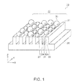
- Fig. 1 is a perspective view showing a part of a sensor chip according to a first embodiment of the invention.
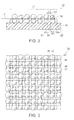
- Fig. 2 is a cross-sectional view of the sensor chip according to the first embodiment.
- Fig. 3 is a plan view showing a part of a sensor chip according to a second embodiment of the invention.
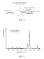
- Fig. 4 is an explanatory diagram of Raman spectroscopy.
- Fig. 5 is a spectrum chart showing a measurement example assuming that the detection target substance is acetaldehyde.
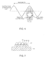
- Fig. 6 is an explanatory diagram of an enhanced electric field formed when irradiating the fine metal particles with light.
- Fig. 7 is a cross-sectional view showing a part of a sensor chip according to a third embodiment of the invention.
- Fig. 8 is an explanatory diagram of an enhanced electric field formed when irradiating the metal nano-particles according to a modified example with light.
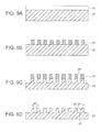
- Figs. 9A through 9D are cross-sectional diagrams showing a principal manufacturing process of the sensor chip.
- Figs. 10E and 10F are cross-sectional diagrams showing the principal manufacturing process of the sensor chip.
- Fig. 11 is a system explanatory diagram showing a rough outline of an optical interference exposure device using an ultraviolet laser.
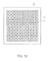
- Fig. 12 is a layout diagram showing a layout configuration of the sensor chip on a sensor substrate.
- Fig. 13 is a configuration diagram showing an example of a configuration of a detection device.
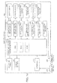
- Fig. 14 is a block diagram showing a configuration of a control system of the detection device.
- Fig. 15 is a diagram showing a state of fine metal particles disposed on a sensor chip using the related art technology.
- Fig. 1 is a perspective view showing a part of a sensor chip according to a first embodiment of the invention
- Fig. 2 is a cross-sectional view of the sensor chip.
- the sensor chip 10 is composed of a relief structure formed on a surface of a substrate 20, and an aggregate of a number of fine metal particles 30.
- the area composed of the relief structure and the fine metal particles is defined as a sensor section 11.
- the material of the substrate 20 is made of a dielectric substance, and quartz, quartz crystal, glass such as borosilicate glass, silicon, and so on are suitable therefor.
- the substrate which is transparent with respect to the incident light is suitable, and in the case of setting the incident light to the fine metal particle side, the transparent substrate is not necessarily required.
- the relief structure is formed to have a linear grating shape, and is formed by forming protruding sections 22, 23, ..., by digging down recessed sections 24 from the upper surface 21 of the substrate 20 using an etching process.
- the protruding sections 22, 23, ... form a single-dimensional structure in which the protruding sections 22, 23, ..., are each disposed linearly in the Y direction, arranged in the X direction in parallel to each other, and protrude so as to be roughly perpendicular to the upper surface of the substrate 20 (Z direction).
- the relief structure is not limited to the linear arrangement as shown in the drawing, but can also have a concentric circular shape or a spiral shape.
- the average particle diameter of the fine metal particles 30 is preferably equal to or smaller than 200nm with which gravitational sedimentation in the mixture with the dispersion medium described later is hard to occur and which is smaller than the wavelength of the incident light, and is more preferably in a range of 10nm through 100nm.
- the fine metal particles 30 are not required to have particle sizes equal to each other providing the particle sizes are in a range of 10nm through 100nm.
- the distance W1 (the width of the recessed section 24) between the protruding sections adjacent to each other in the relief structure is set to be smaller than the average particle size D1 of the fine metal particles 30. Therefore, there is adopted a structure in which most of the fine metal particles 30 are supported by upper ridgelines 22a, 23a of the respective protruding sections 22, 23 adjacent to each other instead of being disposed inside the recessed section 24.
- the fine metal particles 30 are arranged in the Y direction along the recessed sections as shown in Fig. 1 .
- the average particle diameter D1 of the fine metal particles 30 and the distance W1 between the protruding sections are set so that the gap L1 between the fine metal particles 30 adjacent to each other in the X direction has a dimension suitable for forming an enhanced electric field due to the surface plasmon resonance.
- the second embodiment is characterized in that the relief structure is formed to have a grid shape having a two-dimensional structure.
- Fig. 3 is a plan view showing a part of the sensor chip according to the second embodiment. It should be noted that the cross-sectional structure can be expressed similarly to Fig. 2 , and is therefore omitted.
- the relief structure has the protruding sections and the recessed sections arranged in each of the vertical and horizontal directions.
- the fine metal particles 30 is arranged to be supported by four apexes at which respective ridgelines of the columnar protruding sections 25, 26, 27, and 28 intersect each other.
- the units are arranged in the vertical and horizontal directions of the substrate 20.
- the portions (white portions in the drawing) other than the protruding sections 25, 26, 27, and 28 are the recessed sections in the present embodiment, it is also possible to adopt the relief structure obtained by exchanging the protruding section and the recessed sections with each other. In such a configuration, the fine metal particles 30 are each supported by the ridgelines of the protruding sections 25, 26, 27, and 28.
- the planar shape of each of the protruding sections can be a rectangle or a circle.
- the average particle diameter D1 of the fine metal particles, the distance W1 between the protruding sections, and the distance L1 between the fine metal particles are set to have the same relationship as in the first embodiment described above.
- Fig. 4 is an explanatory diagram of the Raman spectroscopy
- Fig. 5 is a spectrum chart showing a measurement example assuming that the detection target substance is acetaldehyde
- Fig. 6 is an explanatory diagram of an enhanced electric field formed when irradiating the fine metal particles with light.
- a most part thereof is scattered without being varied in the wavelength as the Rayleigh scattered light.
- a part thereof is scattered as the Raman scattered light (with a wavelength ⁇ - ⁇ ') including information of the molecular vibration of the target molecules. It results that "fingerprint" spectrum of the target molecules (here the acetaldehyde molecules are shown as an example) shown in Fig. 5 can be obtained in the Raman scattered light.
- Fig. 5 shows a measurement example of the spectrum when setting the detection target substance to acetaldehyde, with the lateral axis representing Raman shift (unit: cm-1), and the vertical axis representing signal intensity. Due to the fingerprint spectrum, it is possible to identify the substance thus detected as the acetaldehyde molecules. However, the Raman scattered light (the Raman signal) is extremely faint, and therefore, it is difficult to detect the substance present in only minute amounts. Therefore, the surface plasmon resonance is used for generating the enhanced electric field to thereby enhance the Raman signal.
- Fig. 6 is an explanatory diagram of an enhanced electric field formed when irradiating the fine metal particles with light.
- the surface plasmon resonance denotes the vibration mode of the electron wave causing the coupling with light under the boundary condition unique to the surface of the substance.
- the free electrons existing on the surface of each of the fine metal particles resonate due to the action caused by the electric field of the incident light.
- an enhanced electric field stronger than the electric field of the incident light is formed in the vicinity of the fine metal particles.
- This phenomenon is a phenomenon unique to the metal particles smaller than the wavelength of the light.
- the propagating surface plasmon exists on the metal surface on the one hand
- the localized surface plasmon exists on the metal nanoparticle on the other hand when the localized surface plasmon, namely the surface plasmon localized on the microstructure of the surface, is excited, a remarkably enhanced electric field is induced.
- the phenomenon described above is called localized surface plasmon resonance.
- the fine metal particles are aligned on the substrate 20 to thereby be arranged so as to form the enhanced electric field in the gap between the fine metal particles.
- the Raman scattered light is enhanced in the enhanced electric field, and thus a strong Raman signal can be obtained.
- Such Raman scattered light is referred to as surface enhanced Raman scattered light.
- the Raman spectroscopy can be performed even on the target molecules present in minute amounts. This is the principle of making it possible to detect minute amount of target molecules with high sensitivity.
- the sensor chip 10 is a sensor for detecting the detection target substance using the localized surface plasmon resonance and the surface enhanced Raman scattering. Therefore, according to the first and second embodiments, the fine metal particles 30 are arranged with the directions of the minute gaps formed between the fine metal particles aligned in accordance with the distance between the protruding sections 22, 23 (or the protruding sections 25, 26, 27, and 28) formed on the surface 20a of the substrate 20. Therefore, it results that the localized surface plasmon resonance occurs more efficiently. As a result, the surface enhanced Raman scattering for realizing the high sensitivity is performed, and thus, the sensor chip capable of detecting the substance with high sensitivity can be realized.
- the substrate 20 is made of a dielectric material.
- the sensor chip according to any of the embodiments described above is for enhancing the surface enhanced Raman scattering by the enhanced electric field due to the localized surface plasmon resonance occurring in the periphery thereof in the gap between the fine metal particles to thereby detect the fingerprint spectrum of the detection target substance. Therefore, by using a dielectric material as the material of the substrate 20, the influence of the medium in the periphery of the fine metal particles on the electric field can be eliminated to thereby prevent the peak intensity of the spectrum from being deteriorated.
- the average particle diameter D1 of the fine metal particles 30 is smaller than the wavelength of the incident light, and has a size suitable for forming the enhanced electric field due to the surface plasmon resonance.
- the free electrons existing on the surface of each of the fine metal particles are subjected to the action of the electric field of the incident light to thereby resonate.
- the condition in which the electric dipoles due to the free electrons are aligned is created in the periphery of each of the fine metal particles, and the enhanced electric field stronger than the electric field of the incident light can be formed.
- the distance W1 between the protruding sections adjacent to each other in the relief structure is smaller than the average particle size D1 of the fine metal particles 30.
- the fine metal particles can be arranged with appropriate gaps by the upper ridgelines 22a, 23a of the protruding sections 22, 23 without dropping off in the recessed sections 24.
- the fine metal particles are each made of gold (Au), silver (Ag), copper (Cu), aluminum (Al), platinum (Pt), palladium (Pd), molybdenum (Mo), or chromium (Cr), or alloys or complexes of any of these metals. If those made of the material described above are used as the fine metal particles, it is possible to develop the surface plasmon resonance (SPR), the localized surface plasmon resonance (LSPR), and the surface enhanced Raman scattering (SERS), and in particular, Au or Ag can develop these phenomena strongly, and thus it becomes possible to detect the detection target substance with high sensitivity.
- SPR surface plasmon resonance
- LSPR localized surface plasmon resonance
- SERS surface enhanced Raman scattering
- the third embodiment is characterized by being different from the first and second embodiments in the cross-sectional shape of the relief structure. Therefore, the different point will be explained.
- Fig. 7 is a cross-sectional view showing a part of the sensor chip according to the third embodiment.
- the recessed sections of the relief structure are each formed having tilted walls (a tapered shape) with the bottom width narrower than the width on the upper surface 21 of the substrate 20.
- tilted walls a tapered shape
- Such a shape can be applied to both of the one-dimensional structure of the first embodiment and the two-dimensional structure of the second embodiment described above (the case of the first embodiment is shown in the drawing).
- the fine metal particles 30 are each held by the protruding sections 22, 23 to thereby form a predetermined arrangement structure.
- the recessed sections 24 each have the tapered shape in some cases.
- the recessed sections 24 become easy to manufacture by setting the relationship between the distance W1 between the protruding sections adjacent to each other in the relief structure, the average particle diameter D1 of the fine metal particles 30, and the distance L1 between the fine metal particles similar to the cases of the first and second embodiments described above.
- the modified example is characterized in that the fine metal particles are arranged on the upper surface 21 of the substrate 20 using an inkjet process.
- Fig. 8 is an explanatory diagram of an enhanced electric field formed when irradiating the fine metal particles according to the modified example with the light.
- the sensor chip 10 has the fine metal particles 30 arranged on the substrate surface 20a so as to form a single layer.
- the fine metal particles 30 can be adsorbed to the substrate 20 by dropping a dispersion liquid including the fine metal particles 30 mixed with the dispersion medium onto the substrate surface 20a using the inkjet process, and then evaporate the dispersion medium.
- the fine metal particles 30 are formed on the substrate 20 in an arrangement capable of forming the enhanced electric field in the gaps therebetween in advance.
- the detection target substance the target molecules
- the Raman scattered light is enhanced in the enhanced electric field, and thus a strong Raman signal can be obtained.
- the detection sensitivity is slightly degraded compared to the case of arranging the fine metal particles using the relief structure as in the first and second embodiments, it becomes possible to arrange the fine metal particles to have the distance L1 therebetween suitable for developing the localized surface plasmon resonance.
- Figs. 9A through 9D , 10E, and 10F are cross-sectional diagrams showing a principal manufacturing process of the sensor chip.
- the material of the substrate 20 there can be used quartz, quartz crystal, glass such as borosilicate glass, silicon, and so on.
- the explanation will be presented showing a quartz plate as an example.
- a resist 40 is applied to a surface of the clean substrate 20 with a device such as a spin coater, and is then dried.
- the laser interference exposure is performed thereon for forming a desired relief pattern.
- the optical interference exposure method with an ultraviolet lase can be used.
- the electron beam exposure method offers high flexibility of exposure, but has limitations in mass productivity on the negative side. Therefore, the optical interference exposure device using the ultraviolet laser superior in mass productivity is used here.
- Fig. 11 is a system explanatory diagram showing a rough outline of the optical interference exposure device using the ultraviolet laser.
- the laser beam output from the laser device is folded by a mirror 102 after passing through a shutter 101, and is then branched into two directions by a half mirror 103.
- the ultraviolet laser beams thus branched are folded by mirrors 104, 105, and are then spread by passing through field lenses 106, 107 and pinholes, respectively.
- masks 108, 109 are irradiated with the respective ultraviolet laser beams thus spread to thereby form an interference pattern, and then the substrate 20 (a sensor substrate 70) coated with a resist 40 (see Fig. 9A ) with the interference pattern.
- a variety of patterns of exposure become possible in accordance with the exposure configuration of the interference pattern.
- a continuous-wave YVO4 laser (wavelength of 266nm, maximum power of 200mW) is used as the light source of the interference exposure.
- a positive resist is used, and the film thickness of the resist is set to 10m.
- the exposure pattern of the resist by forming one of the patterns to have a grating shape and forming the other of the patterns to have also a grating shape, a variety of patterns can be formed in accordance with the angle at which the both patterns intersect each other, and the size thereof can be made as small as a half of the laser wavelength.
- a latent image of the interference pattern of the both patterns is formed on the resist 40, and the resist is developed to thereby form a desired pattern ( Fig. 9B ).
- the portions not protected by the resist pattern are etched to thereby form the recessed sections 24 on the substrate 20 ( Fig. 9C ). Further, the resist 40 remaining on the substrate 20 is removed ( Fig. 9D ) .
- the relief structure composed of the protruding sections 22, 23, ..., and the recessed sections 24 is formed.
- the distance W1 (the width of the recessed section 24) between the protruding sections adjacent to each other is set to be smaller than the average particle size D1 of the fine metal particles 30.
- the fine metal particles 30 are arranged on the relief structure using the inkjet process.
- the portion provided with the relief structure located at roughly central part of the substrate 20 corresponds to the sensor section 11, and the dispersion liquid 80 including the fine metal particles is ejected on the roughly central portion thereof using an inkjet device. It should be noted that the ejection is performed so that the size of the spread of the dispersion liquid after ejected on the relief structure becomes smaller than the forming area of the relief structure.
- the dispersion liquid is landed on the sensor section 11 so as to rise therefrom due to the surface tension. Subsequently, the dispersion medium is gradually dried while penetrating into the recessed sections 24 of the relief structure, and is thus removed.
- the dispersion medium can be removed by heated-air drying.
- the evaporation process of the dispersion medium most of the fine metal particles dispersed therein are captured by the recessed sections 24 with the upper ridgelines 22a, 23a of the protruding sections 22, 23 of the relief structure.
- the adsorption of the fine metal particles 30 to the relief structure is caused by the evaporation of the dispersion medium from the upper surface, and the action of the dispersion medium percolating through the recessed sections 24 of the relief structure to seep outside.
- a rotatable vacuum chamber is made vacuum while circulating the liquid composed of alkyl naphthalene with low vapor pressure and polyamine as a lipophilic surfactant on the inside wall of the vacuum chamber.
- the degree of vacuum is about 102 (Pa).
- the fine metal particles are evaporated from the evaporation source capable of evaporating the metal contained in a melting pot with a heater (a resistive heater or an inductive heater) existing therein, then captured by the liquid circulated on the inner wall of the vacuum chamber, and then accumulated in the lower part of the vacuum chamber with the rotation as a liquid.
- the material of the fine metal particles Au, Ag, A1, Cu, Pd, Cr, Pt, and so on are suitable.
- the particle diameter thereof is preferably equal to or smaller than 200nm with which gravitational sedimentation is hard to occur and which is smaller than the wavelength of the incident light, and is more preferably in a range of 10nm through 100nm.
- silver nano-particles having a property of strongly developing the SPR, LSPR, and SERS will be explained.
- the silver nano-particles it is preferable to use silver nano-particles having an average particle diameter of no larger than 100nm generated by adding iron sulfate to a silver nitrate solution under existence of sodium citrate to thereby reduce the silver ions. It is preferable that iron sulfate and sodium citrate are mixed with each other in advance, and then the silver nitrate solution is poured in the mixed solution under the room temperature to thereby reduce the silver nitrate.
- the silver concentration in the silver nitrate solution is appropriately in a range of 1g/L through 200g/L, and the amount of iron sulfate is only required to be an amount with which the silver nitrate can sufficiently be reduced.
- the amount of sodium citrate is preferably in a range of 2 through 7 times of the number of moles of silver.
- the mixture of the silver nitrate solution and the iron sulfate solution is preferably performed by pouring the solution at 5 through 20ml/min in every supply nozzle. After the mixture, the solutions are agitated to thereby be reacted each other evenly. Silver is reduced due to the reaction, and a silver colloidal solution including silver ultrafine particles (silver nano-particles) having a particle diameter of nanometer size can be obtained. By performing solid-liquid separation on the silver colloidal solution, and then cleansing the solid content thus separated with sodium citrate, a silver colloidal liquid having the silver nano-particles dispersed can be obtained.
- the dispersion liquid of the silver nano-particles can be manufactured by, for example, dispersing material fine particles in an appropriate dispersion medium to thereby obtain the dispersion liquid, and then adding thiol compound into the dispersion liquid.
- concentration of the fine metal particles to the dispersion medium is preferably in a range of 1 through 50% by weight, and is more preferably in a range of 4 through 20% by weight. If the percentage by weight of the fine metal particles is too low, the density of the fine metal particles formed becomes lower, and the enhanced electric field due to the localized surface plasmon resonance becomes weaker. If it is too high, in contrast, ejection of the droplets becomes unstable.
- the dispersion medium there can be cited, for example, alcohols such as methanol, ethanol or isopropanol, butanol, octanol, ethylene glycol, diethylene glycol, or glycerine, cellosolveTM such as methyl cellosolve, ethyl cellosolve, or phenyl cellosolve, esters such as methyl acetate, ethyl acetate, butyl acetate, or ethyl formate, ketones such as acetone, methyl ethyl ketone, diethyl ketone, methyl isobutyl ketone, methyl isopropyl ketone, or cyclohexanon, aliphatic hydrocarbons (paraffinic hydrocarbons) such as pentane, hexane, or octane, alicyclic hydrocarbons such as cyclohexane or methyl cyclohexane, aromatic
- the dispersion medium with high vapor pressure easily evaporates in the vicinity of the nozzle to easily cause clogging of the nozzle, it is required to take a device of, for example, covering the nozzle with a cap for preventing the evaporation except the period of ejecting the droplets.
- the method of dispersing the fine metal particles into the dispersion medium described above there can be cited, for example, a method of dispersing them by mechanical impact or shear using a beads mill, a rocking mill, a homogenizer, and so on, and a method of dispersing them by a cavitation force of an ultrasonic wave, a high-pressure homogenizer and so on.
- the dispersion method using an ultrasonic device, in particular, an ultrasonic homogenizer is frequently used.
- the frequency range a range of 2 through 100kHz is preferable, a range of 2 through 50kHz is more preferable, and a range of 10 through 40kHz is particularly preferable.
- the irradiation of the ultrasonic wave can be performed continuously or intermittently, if the irradiation time is long, the intermittent irradiation is more preferable. This is because there is concern that the heating due to the continuous irradiation of the ultrasonic wave for a long time exerts a harmful influence on the dispersion of the particles.
- the inkjet method there are proposed a variety of types of methods. Broadly, they are classified into an electrostatic method, a piezoelectric method, and a film boiling inkjet method.
- the principle of the electrostatic method is that when a drive signal is provided to an electrostatic gap as an actuator, a diaphragm in a cavity is displaced to cause pressure variation in the cavity, and an ink droplet is ejected from the nozzle due to the pressure variation.
- the principle of the piezoelectric method is that when a drive signal is provided to a piezoelectric element as an actuator, a diaphragm in a cavity is displaced to cause pressure variation in the cavity, and an ink droplet is ejected from the nozzle due to the pressure variation.
- the principle of the film boiling inkjet method is that a microscopic heater is provided inside the cavity, and is instantaneously heated to 300[] C or higher to thereby make the ink become in the film boiling state to generate a bubble, thus causing the pressure variation which makes the ink droplet be ejected from the nozzle.
- a microscopic heater is provided inside the cavity, and is instantaneously heated to 300[] C or higher to thereby make the ink become in the film boiling state to generate a bubble, thus causing the pressure variation which makes the ink droplet be ejected from the nozzle.
- either type of inkjet device can be used.
- the sensor chip 10 is manufactured using a batch process in which a number of sensor chips are arranged on a large-sized sensor substrate.
- Fig. 12 is a layout diagram showing a layout configuration of the sensor chip on the sensor substrate.
- a number of relief structures are formed on the sensor substrate 70 using the method (see Figs. 9A through 9D , 10E, and 10F ) described above. Each aggregate of these relief structures corresponds to the sensor section 11.
- the dispersion liquid having the fine metal particles dispersed therein is ejected on each of the relief structures using the inkjet device to thereby form the sensor chips 10.
- the sensor substrate 70 is fixed to an X-Y stage of the inkjet device, and a number of sensor chips 10 are arranged on the sensor substrate 70 as shown in Fig. 12 .
- the X-Y stage is moved to a position where the dispersion liquid is ejected on the central portion of one of the sensor chips 10 one-by-one, and is then stopped once for positioning, and then the dispersion liquid is ejected from the nozzle selected. Subsequently, the X-Y stage is moved to the position corresponding to the central portion of the next one of the sensor chips 10, and then the dispersion liquid is ejected in a similar manner. By repeating the operation described above, the dispersion liquid is ejected on all of the sensor chips 10 (the sensor sections 11). Subsequently, the dispersion medium is dried to thereby arrange the fine metal particles in each of the relief structures.
- the sensor substrate 70 is cut into individual sensor chips 10 using a dicing apparatus or the like, and thus the sensor chip 10 shown in Figs. 1 and 2 is formed.
- the relief structure is formed using the laser interference exposure process and the etching process.
- the arrangement of the relief pattern can be formed as, for example, a pattern of a one-dimensional structure or a pattern of a two-dimensional structure using such processes. Further, when ejecting the dispersion liquid to the upper part of the relief structure, the fine metal particles 30 are arranged along the upper ridgelines of each of the projecting sections, and during the process of drying (or heated-air drying) to remove the dispersion medium, the fine metal particles are arranged along the pattern of the relief structure thus formed.
- the process of ejecting the dispersion liquid having the fine metal particles 30 dispersed in the dispersion medium on the upper part of the relief structure is performed using the inkjet device.
- the fine metal particles of the related art there has been known a method of dropping a droplet of the dispersion liquid on the substrate and then centrifugally spreading it in a thin and even manner using a device such as a spin coater.
- a state of fine metal particles disposed on a sensor chip using the related art technology is shown in Fig. 15 .
- the size of the spread after ejecting the dispersion liquid 80 is set to be smaller than the forming area of the relief structure.
- the dispersion liquid is attached so as to rise with respect to the sensor section due to the surface tension.
- the dispersion medium is gradually dried while penetrating into the recessed sections of the relief structure.
- a large proportion of the fine metal particles dispersed therein is captured by the recessed sections in the relief structure. This is caused by the evaporation of the dispersion medium and the action of the dispersion medium percolating through the recessed sections of the relief structure to seep outside.
- most of the fine metal particles included in the dispersion liquid can be left in the relief structure, and thus the sensor chips can efficiently be manufactured without incurring waste.
- Fig. 13 is a configuration diagram showing an example of a configuration of the detection device.
- the detection device 200 is composed of consumables such as the sensor chip 10 and a suction channel 220 replaced in each detection, and a main body section which can be used repeatedly.
- the main body section is mainly composed of a sensor section cover 201 which can be opened and closed so as to store and replace the consumables, a discharge section 203, a housing 204 of the main body, a detection section including a light source 205, lenses 206, 207, and 209, a filter 210, a spectroscope 211, a light receiving element 212, and so on, a signal processing/control section 213 for processing the signal thus detected and controlling the detection section, a power supply section 214 for supplying the power, a connection sections 215, 216 for establishing the interface with the outside, and so on.
- the shape of the channel for sucking in and discharging the gaseous sample is considered so that the external light can be prevented from entering the sensor section and that the fluid resistance to the gaseous sample decreases.
- the external light By preventing the external light from entering the sensor section, the light other than the Raman scattered light, which becomes noise, is not input, and the S/N ratio of the signal is improved. It becomes necessary to select the material, color, and surface shape of the material forming the channel so as to be difficult to reflect the light in addition to the shape of the channel.
- the fluid resistance to the gaseous sample decreases, a large amount of gaseous sample in the vicinity of the detection device 200 can be collected, and the detection with high sensitivity becomes possible.
- these channels so as to have a smooth shape by eliminating the apexes as much as possible, accumulation of the gaseous sample can be eliminated.
- the discharge section 203 it is also necessary to select a fan motor or a pump having static pressure and air volume corresponding to the channel resistance.
- the sensor chip 10 is irradiated with the light from the light source (the laser source) 205 of a linearly polarized light with a single wavelength, then the surface enhanced Raman scattered (SERS) light is radiated from the sensor chip 10, then collected by the lens 207, and then enters the light receiving element 212 with a half mirror 208. Since the light includes the Rayleigh beam having a wavelength equal to the wavelength of the incident light from the light source, the SERS light, and so on, the Rayleigh beam is removed by the filter 210, and then the light enters the spectroscope 211.
- the fingerprint spectrum unique to the target substance can be obtained by the spectroscope 211 and the light receiving element 212, and by matching the spectrum with the data held therein in advance, the target substance can be identified.
- the target substance is naturally diffused and discharged.
- the process of actively promoting the discharge using the discharge section 203 and then replacing the sensor chip 10 and so on having been used in preparation for the subsequent detection is performed in preparation for the subsequent detection.
- the method of replacing the sensor chip 10 will be explained.
- the sensor section cover 201 is opened, and then the consumables integrally including the sensor chip 10, the suction channel 220, the dust filter 230, and so on are taken out.
- a sensor chip detector 240 When new consumables is set there along a positioning member of a part of the sensor chip 10 after releasing the sealing section of the suction port of the consumables, a sensor chip detector 240 operates, and it is determined that the detection device 200 is in the state in which the detection device 200 can perform the detection.
- a primary cell or a secondary cell can be used as the power supply section.
- the primary cell an opening section (not shown) for replacing the battery is disposed in the lower part of the housing 204 of the main body, and if battery run out is displayed on the main body display (not shown), the battery can be replaced.
- a connection section 215 is located on the lower part of the housing 204 of the main body, and if the buttery run out is displayed on the main body display, a battery charger is connected to the connection section 215 to thereby charge the secondary battery, and if completion of charge is displayed, the detection device 200 can be used again after removing the battery charger.
- Fig. 14 is a block diagram showing the configuration of the control system of the detection device. It should be noted that Fig. 13 is also referred to.
- an operation panel 250 On the surface of the detection device 200, there are provided an operation panel 250, a display section 251, the connection section 215 for the interface with the outside, and the power supply section 214.
- the connection section 216 for the battery charge is also provided.
- the sensor chip 10 In the inside of the sensor section cover 201 in the upper part of the main body, there are disposed the sensor chip 10, and the sensor chip detector 240 for detecting presence or absence of the sensor chip 10, and reading the code of the sensor chip 10, and the information thereof is transmitted to a central processing unit (CPU) constituting the signal processing/control section 213 via a sensor chip detection circuit 234, and the determination is performed. Since this state is a state in which the preparation for detection is completed, the display signal representing the ready state is output from the CPU to the display section 251. The operator looking at the display outputs the instruction signal representing start of detection from the operation panel 250 to the CPU.
- CPU central processing unit
- the CPU When the CPU receives the signal representing start of detection, the CPU firstly outputs the signal for operating the light source to a light source driver circuit 231 to thereby operate the light source 205.
- the light source 205 incorporates a temperature sensor and a light intensity sensor, and the information thereof is transmitted to the CPU, and then the CPU determines whether or not the operation is in a stable state.
- the instruction signal of making the discharge section 203 operate is transmitted from the CPU to a suction section driver circuit 235 in order to guide the gaseous sample including the target substance to be detected to the vicinity of the surface of the sensor chip 10, and the gaseous sample enters the suction port 202, passes through the suction channel 220, the sensor chip space, and the discharge channel 221, and is then discharged to the outside.
- the light source 205 (the laser source) for radiating the stable linearly polarized light with a single wavelength
- the light source 205 is driven by the light source driver circuit 231 in accordance with the signal from the CPU, and radiates the laser beam.
- the sensor chip 10 is irradiated with the laser beam, and thus the Rayleigh beam and the surface enhanced Raman scattered (SERS) light enter the light receiving side via the lenses 206, 207, and the half mirror 208.
- SERS surface enhanced Raman scattered
- the SERS light alone enters the spectroscope 211.
- the spectroscope 211 is controlled by a spectroscope driver circuit 232.
- the band ( ⁇ 1 through ⁇ 2) and the half bandwidth of the light transmitted therethrough are set, and the intensity of the optical signal corresponding to the half bandwidth is repeatedly detected by the light receiving element 212 while changing the wavelength of the light transmitted therethrough from ⁇ 1 to ⁇ 2 by the half bandwidth, and then the intensity of the optical signal is converted into an electrical signal by a light receiving circuit 233. According to such an operation as described above, it results that the spectrum of the SERS light thus detected can be obtained.
- the spectrum of the SERS light of the target substance thus obtained is compared with the spectrum data stored in the ROM of the signal processing/control section 213 to thereby making a judgment on whether or not the target substance is the objective substance, and thus the identification of the substance is performed.
- the result information is transmitted from the CPU to the display section 251, and is then displayed.
- it is arranged to transmit the information from the connection section 215 based on an interface standard determined in advance.
- a primary cell As the power supply section 214, a primary cell, a secondary cell, and so on can be used.
- the CPU compares the information stored in the ROM and the voltage information of the primary cell thus obtained with each other to determine whether or not the voltage of the primary cell becomes lower than a predetermined voltage, and if it is lower than the predetermined voltage, the display for the battery replacement is displayed on the display section 251. It is therefore possible for the operator to replace the primary cell and then use the detection device again with reference to the display.
- the CPU compares the information stored in the ROM and the voltage information of the secondary cell thus obtained with each other to determine whether or not the voltage of the secondary cell becomes lower than a predetermined voltage, and if it is lower than the predetermined voltage, the display representing that the battery charge is necessary is displayed on the display section 251. With reference to the display, the operator connects the battery charger to the connection section 216 and performs the battery charge until the predetermined voltage is reached, and thus the detection device can be used repeatedly.
- the fine metal particles having the size in the order of several nanometers are arranged on the sensor chip 10 so as to be aligned in the direction of the minute gaps, and it results that the localized surface plasmon resonance excited by irradiating the fine metal particles with the laser beam occurs more efficiently. As a result, the surface enhanced Raman scattering is performed, and thus, the detection device capable of detecting the substance with high sensitivity can be realized.
- detection of a variety of detection target substances can be performed.
- the detection target substances will hereinafter be cited as an example.
- VOC volatile organic compound
Landscapes
- Physics & Mathematics (AREA)
- Health & Medical Sciences (AREA)
- Chemical & Material Sciences (AREA)
- General Physics & Mathematics (AREA)
- General Health & Medical Sciences (AREA)
- Life Sciences & Earth Sciences (AREA)
- Analytical Chemistry (AREA)
- Biochemistry (AREA)
- Immunology (AREA)
- Pathology (AREA)
- Spectroscopy & Molecular Physics (AREA)
- Engineering & Computer Science (AREA)
- Nuclear Medicine, Radiotherapy & Molecular Imaging (AREA)
- Nanotechnology (AREA)
- Mathematical Physics (AREA)
- Theoretical Computer Science (AREA)
- Investigating, Analyzing Materials By Fluorescence Or Luminescence (AREA)
- Investigating Or Analysing Materials By Optical Means (AREA)
Applications Claiming Priority (1)
| Application Number | Priority Date | Filing Date | Title |
|---|---|---|---|
| JP2010287189A JP5614278B2 (ja) | 2010-12-24 | 2010-12-24 | センサーチップ、センサーチップの製造方法、検出装置 |
Publications (2)
| Publication Number | Publication Date |
|---|---|
| EP2469598A2 true EP2469598A2 (de) | 2012-06-27 |
| EP2469598A3 EP2469598A3 (de) | 2013-09-18 |
Family
ID=45540748
Family Applications (1)
| Application Number | Title | Priority Date | Filing Date |
|---|---|---|---|
| EP20110195171 Withdrawn EP2469598A3 (de) | 2010-12-24 | 2011-12-22 | Sensorchip, Erfassungsvorrichtung und Verfahren zur Herstellung eines Sensorchips |
Country Status (6)
| Country | Link |
|---|---|
| US (1) | US9228945B2 (de) |
| EP (1) | EP2469598A3 (de) |
| JP (1) | JP5614278B2 (de) |
| KR (1) | KR20120073138A (de) |
| CN (1) | CN102590088A (de) |
| TW (1) | TWI521196B (de) |
Cited By (6)
| Publication number | Priority date | Publication date | Assignee | Title |
|---|---|---|---|---|
| JP2013190376A (ja) * | 2012-03-15 | 2013-09-26 | Seiko Epson Corp | センサーチップおよびその製造方法並びに検出装置 |
| EP2884266A4 (de) * | 2012-08-10 | 2016-08-10 | Hamamatsu Photonics Kk | Herstellungsverfahren für ein oberflächenverstärktes ramanstreuungselement |
| US9863884B2 (en) | 2012-08-10 | 2018-01-09 | Hamamatsu Photonics K.K. | Surface-enhanced Raman scattering element, and method for producing same |
| US9863883B2 (en) | 2012-08-10 | 2018-01-09 | Hamamatsu Photonics K.K. | Surface-enhanced raman scattering element |
| CN111795946A (zh) * | 2020-06-18 | 2020-10-20 | 浙江大学 | 一种全介质bic结构的相位传感及荧光/拉曼增强芯片 |
| US12411090B2 (en) * | 2023-03-16 | 2025-09-09 | King Fahd University Of Petroleum And Minerals | Electrochemical sensor for detecting hydroxycarbamide |
Families Citing this family (43)
| Publication number | Priority date | Publication date | Assignee | Title |
|---|---|---|---|---|
| JP5945192B2 (ja) * | 2012-08-10 | 2016-07-05 | 浜松ホトニクス株式会社 | 表面増強ラマン散乱ユニット |
| JP5921380B2 (ja) * | 2012-08-10 | 2016-05-24 | 浜松ホトニクス株式会社 | 表面増強ラマン散乱ユニット |
| CN108827928B (zh) * | 2012-08-10 | 2021-12-24 | 浜松光子学株式会社 | 表面增强拉曼散射单元及其使用方法 |
| EP4033222A1 (de) | 2012-08-10 | 2022-07-27 | Hamamatsu Photonics K.K. | Oberflächenverstärkte ramanstreuungseinheit |
| JP6058313B2 (ja) | 2012-08-10 | 2017-01-11 | 浜松ホトニクス株式会社 | 表面増強ラマン散乱ユニット |
| US10633734B2 (en) | 2012-10-05 | 2020-04-28 | California Institute Of Technology | Optical sensor for analyte detection |
| WO2014055951A1 (en) * | 2012-10-05 | 2014-04-10 | California Institute Of Technology | Optical sensor for analyte detection |
| JP6063221B2 (ja) * | 2012-11-22 | 2017-01-18 | 上村工業株式会社 | めっき液中の金濃度の定量方法、および金濃度定量装置 |
| TWI500921B (zh) | 2013-01-14 | 2015-09-21 | Ind Tech Res Inst | 光學感測晶片 |
| US8711351B1 (en) * | 2013-01-29 | 2014-04-29 | Hewlett-Packard Development Company, L.P. | Scattering spectroscopy employing hotspot-aligned nanopores |
| JP6396012B2 (ja) * | 2013-10-31 | 2018-09-26 | 富士電機株式会社 | 光増強素子 |
| US9383300B2 (en) * | 2014-03-19 | 2016-07-05 | Akrometrix Inc. | Precision convection system |
| CN107004913B (zh) * | 2014-04-08 | 2019-10-11 | 英斯普罗恩传感器系统公司 | 具有传感器的电池 |
| CN104359867A (zh) * | 2014-10-27 | 2015-02-18 | 李博 | 一种以钯为靶材制备表面等离子体共振芯片的方法 |
| JP6456683B2 (ja) * | 2014-12-25 | 2019-01-23 | 富士電機株式会社 | 光増強素子及び分析装置 |
| CA2991532C (en) * | 2015-08-04 | 2024-03-05 | Abaxis, Inc. | Signal amplification in solution-based plasmonic specific-binding partner assays |
| CN106468648B (zh) | 2015-08-19 | 2019-09-10 | 财团法人工业技术研究院 | 微粒子侦测器及筛选元件的制造方法 |
| US10121673B2 (en) | 2015-08-19 | 2018-11-06 | Industrial Technology Research Institute | Miniaturize particulate matter detector and manufacturing method of a filter |
| JP6613736B2 (ja) * | 2015-09-07 | 2019-12-04 | セイコーエプソン株式会社 | 物質検出方法および物質検出装置 |
| US10648915B2 (en) | 2015-11-30 | 2020-05-12 | Hewlett-Packard Development Company, L.P. | Substance detection device |
| CN105576497A (zh) * | 2016-03-01 | 2016-05-11 | 中国科学院半导体研究所 | 表面增强的相干反斯托克斯拉曼散射的结构 |
| KR101776103B1 (ko) * | 2016-04-01 | 2017-09-08 | 한국생산기술연구원 | 합성수지를 이용한 sers 기판 및 이의 제조방법 |
| TWI597910B (zh) * | 2016-10-03 | 2017-09-01 | 國立交通大學 | 光學元件、壓力感測元件以及壓力感測裝置 |
| CN106896095B (zh) * | 2017-01-11 | 2019-08-06 | 四川大学 | 复合表面等离子体共振及表面增强拉曼的显微成像技术 |
| CN118275398A (zh) | 2017-01-30 | 2024-07-02 | 硕腾服务有限责任公司 | 基于溶液的等离子体振子特异性结合配偶体测定和金属纳米结构 |
| CN109470681B (zh) * | 2017-09-08 | 2022-02-08 | 清华大学 | 一种分子检测方法 |
| CN109580750A (zh) * | 2017-09-28 | 2019-04-05 | 中国科学院苏州纳米技术与纳米仿生研究所 | 一种可穿戴汗液传感器芯片、装置及其制备方法与应用 |
| JP6954151B2 (ja) * | 2018-01-25 | 2021-10-27 | 王子ホールディングス株式会社 | 分析用基板およびその製造方法 |
| JP6954152B2 (ja) * | 2018-01-25 | 2021-10-27 | 王子ホールディングス株式会社 | 分析用基板 |
| CN208399384U (zh) * | 2018-01-30 | 2019-01-18 | 苏州天际创新纳米技术有限公司 | 一种sers单元、sers芯片及sers检测系统 |
| CN108802005B (zh) * | 2018-06-05 | 2021-08-24 | 河海大学常州校区 | 基于粒子-波导耦合结构的拉曼散射增强基底及制备方法 |
| CN110441284B (zh) * | 2019-07-23 | 2022-02-15 | 海南大学 | 一种可用于痕量检测的表面增强拉曼散射芯片的制备方法及所得产品和应用 |
| US12272607B2 (en) | 2020-01-09 | 2025-04-08 | Applied Materials, Inc. | Method of enhancing contrast while imaging high aspect ratio structures in electron microscopy |
| CN111239207B (zh) * | 2020-03-03 | 2022-12-23 | 电子科技大学中山学院 | 一种由金属氧化物多孔薄膜和孔洞构成的复合结构气体传感器 |
| CN111443072B (zh) * | 2020-04-30 | 2023-12-22 | 苏州翊清环境科技有限公司 | 病毒检测用拉曼芯片、制备方法、及病毒快速检测方法 |
| IT202000009727A1 (it) * | 2020-05-04 | 2021-11-04 | Dg Group S P A | Sensore colorimetrico per la rilevazione di batteri e/o virus |
| EP4068234B1 (de) * | 2021-03-31 | 2024-11-13 | Carrier Fire & Security EMEA BV | Ansaugsystem zur erkennung von krankheitserregern |
| US11959859B2 (en) | 2021-06-02 | 2024-04-16 | Edwin Thomas Carlen | Multi-gas detection system and method |
| US11664283B2 (en) * | 2021-08-20 | 2023-05-30 | Tokyo Electron Limited | Raman sensor for supercritical fluids metrology |
| CA3207609A1 (en) * | 2022-05-18 | 2023-11-18 | Wonkyeong LEE | Heating structure and aerosol generating device including the same |
| TWI827170B (zh) * | 2022-07-29 | 2023-12-21 | 四方仁禾半導體股份有限公司 | 表面增強型拉曼光譜晶片及其檢測系統 |
| CN115980015A (zh) * | 2022-11-28 | 2023-04-18 | 嘉兴学院 | 表面增强拉曼活性基底及其制备方法和应用 |
| KR102897525B1 (ko) * | 2025-05-30 | 2025-12-08 | 경찰대학 산학협력단 | 인공지능 기반 지능형 마약류 탐지 시스템 |
Citations (1)
| Publication number | Priority date | Publication date | Assignee | Title |
|---|---|---|---|---|
| JP2000356587A (ja) | 1999-06-14 | 2000-12-26 | Inst Of Physical & Chemical Res | 局在プラズモン共鳴センサー |
Family Cites Families (26)
| Publication number | Priority date | Publication date | Assignee | Title |
|---|---|---|---|---|
| US20040023293A1 (en) * | 1999-09-27 | 2004-02-05 | Kreimer David I. | Biochips for characterizing biological processes |
| US7164533B2 (en) * | 2003-01-22 | 2007-01-16 | Cyvera Corporation | Hybrid random bead/chip based microarray |
| JP3923436B2 (ja) * | 2003-02-12 | 2007-05-30 | 富士フイルム株式会社 | センサチップおよびそれを用いたセンサ並びにセンサチップの作製方法 |
| JP4109205B2 (ja) * | 2004-01-07 | 2008-07-02 | 富士フイルム株式会社 | 被検体検出方法 |
| JP2005200677A (ja) * | 2004-01-13 | 2005-07-28 | Fuji Photo Film Co Ltd | 金属微粒子の作製方法 |
| EP1580305A3 (de) | 2004-03-23 | 2008-01-16 | FUJIFILM Corporation | Feinstrukturierte Körperoberfläche und Verfahren zu deren Herstellung |
| RU2361193C2 (ru) * | 2004-05-19 | 2009-07-10 | Вп Холдинг, Ллс | Оптический датчик с многослойной плазмонной структурой для усовершенствованного обнаружения химических групп посредством sers |
| JP2006038506A (ja) * | 2004-07-23 | 2006-02-09 | Fuji Photo Film Co Ltd | 微細構造体 |
| US20060275541A1 (en) | 2005-06-07 | 2006-12-07 | Weimer Wayne A | Systems and method for fabricating substrate surfaces for SERS and apparatuses utilizing same |
| EP1891414A4 (de) * | 2005-06-14 | 2010-04-21 | Fujifilm Corp | Sensor, mehrkanalsensor, wahrnehmungsvorrichtung und verfahren |
| WO2007040219A1 (ja) * | 2005-10-04 | 2007-04-12 | Intellectual Property Bank Corp. | ナノアレイdnaチップ |
| JP2007171003A (ja) * | 2005-12-22 | 2007-07-05 | Fujifilm Corp | 質量分析用基板並びに分析方法および装置 |
| US20080003576A1 (en) | 2006-06-30 | 2008-01-03 | Jingwu Zhang | Assay platforms and detection methodology using surface enhanced Raman scattering (SERS) upon specific biochemical interactions |
| JP2008026109A (ja) * | 2006-07-20 | 2008-02-07 | Fujifilm Corp | 微細構造体及びその製造方法、センサデバイス及びラマン分光用デバイス |
| JP4993360B2 (ja) * | 2007-06-08 | 2012-08-08 | 富士フイルム株式会社 | 微細構造体及びその製造方法、光電場増強デバイス |
| US20090097022A1 (en) | 2007-08-24 | 2009-04-16 | Dynamic Throughput Inc. | Discovery tool with integrated microfluidic biomarker optical detection array device and methods for use |
| US7952705B2 (en) | 2007-08-24 | 2011-05-31 | Dynamic Throughput Inc. | Integrated microfluidic optical device for sub-micro liter liquid sample microspectroscopy |
| JP2009109395A (ja) * | 2007-10-31 | 2009-05-21 | Fujifilm Corp | 微細構造体の作製方法、微細構造体、ラマン分光用デバイス、ラマン分光装置、分析装置、検出装置、および質量分析装置 |
| US8506849B2 (en) | 2008-03-05 | 2013-08-13 | Applied Nanotech Holdings, Inc. | Additives and modifiers for solvent- and water-based metallic conductive inks |
| US8559002B2 (en) | 2008-03-20 | 2013-10-15 | Drexel University | Method for the formation of SERS substrates |
| WO2009136869A1 (en) * | 2008-05-05 | 2009-11-12 | Agency For Science, Technology And Research | Sensor chip for biological and chemical sensing |
| US7787117B1 (en) | 2008-06-24 | 2010-08-31 | Bruker Optics, Inc. | Method and apparatus for in situ measurement of material properties by surface enhanced raman spectroscopy |
| US20100053605A1 (en) * | 2008-07-25 | 2010-03-04 | Lynntech, Inc. | Gas sampling device and method for collection and in-situ spectroscopic interrogation of vapors and aerosols |
| US8243271B2 (en) | 2009-02-26 | 2012-08-14 | Pchem Associates, Inc. | Methods for fabricating analytical substrates using metallic nanoparticles |
| US8427639B2 (en) * | 2009-05-07 | 2013-04-23 | Nant Holdings Ip, Llc | Surfaced enhanced Raman spectroscopy substrates |
| US9797842B2 (en) * | 2010-12-08 | 2017-10-24 | Osaka Prefecture University Public Corporation | Device and method utilizing a metallic nanoparticle assembly structure for detecting a target substance |
-
2010
- 2010-12-24 JP JP2010287189A patent/JP5614278B2/ja not_active Expired - Fee Related
-
2011
- 2011-12-20 CN CN2011104306008A patent/CN102590088A/zh active Pending
- 2011-12-21 TW TW100147815A patent/TWI521196B/zh not_active IP Right Cessation
- 2011-12-22 EP EP20110195171 patent/EP2469598A3/de not_active Withdrawn
- 2011-12-22 US US13/334,861 patent/US9228945B2/en not_active Expired - Fee Related
- 2011-12-23 KR KR20110141105A patent/KR20120073138A/ko not_active Withdrawn
Patent Citations (1)
| Publication number | Priority date | Publication date | Assignee | Title |
|---|---|---|---|---|
| JP2000356587A (ja) | 1999-06-14 | 2000-12-26 | Inst Of Physical & Chemical Res | 局在プラズモン共鳴センサー |
Non-Patent Citations (2)
| Title |
|---|
| HYEON SUK SHIN ET AL: "Direct patterning of silver colloids by microcontact printing: possibility as SERS substrate array", VIBRATIONAL SPECTROSCOPY, ELSEVIER SCIENCE, AMSTERDAM, NL, vol. 29, no. 1-2, 5 July 2002 (2002-07-05), pages 79 - 82, XP002365870, ISSN: 0924-2031, DOI: 10.1016/S0924-2031(01)00186-2 * |
| MANUEL A. FIGUEROA ET AL: "Development of surface-enhanced Raman scattering (SERS) substrates using nanoparticle-based printing inks", OPTICAL SENSING II, vol. 6866, 7 February 2008 (2008-02-07), 1000 20TH ST. BELLINGHAM WA 98225-6705 USA, pages 686610-1 - 686610-6, XP055292623, ISSN: 0277-786X, ISBN: 978-1-62841-971-9, DOI: 10.1117/12.764577 * |
Cited By (8)
| Publication number | Priority date | Publication date | Assignee | Title |
|---|---|---|---|---|
| JP2013190376A (ja) * | 2012-03-15 | 2013-09-26 | Seiko Epson Corp | センサーチップおよびその製造方法並びに検出装置 |
| EP2884266A4 (de) * | 2012-08-10 | 2016-08-10 | Hamamatsu Photonics Kk | Herstellungsverfahren für ein oberflächenverstärktes ramanstreuungselement |
| US9696202B2 (en) | 2012-08-10 | 2017-07-04 | Hamamatsu Photonics K.K. | Method for making surface enhanced Raman scattering device |
| US9863884B2 (en) | 2012-08-10 | 2018-01-09 | Hamamatsu Photonics K.K. | Surface-enhanced Raman scattering element, and method for producing same |
| US9863883B2 (en) | 2012-08-10 | 2018-01-09 | Hamamatsu Photonics K.K. | Surface-enhanced raman scattering element |
| EP2884266B1 (de) * | 2012-08-10 | 2021-12-01 | Hamamatsu Photonics K.K. | Herstellungsverfahren für ein oberflächenverstärktes ramanstreuungselement |
| CN111795946A (zh) * | 2020-06-18 | 2020-10-20 | 浙江大学 | 一种全介质bic结构的相位传感及荧光/拉曼增强芯片 |
| US12411090B2 (en) * | 2023-03-16 | 2025-09-09 | King Fahd University Of Petroleum And Minerals | Electrochemical sensor for detecting hydroxycarbamide |
Also Published As
| Publication number | Publication date |
|---|---|
| EP2469598A3 (de) | 2013-09-18 |
| KR20120073138A (ko) | 2012-07-04 |
| US9228945B2 (en) | 2016-01-05 |
| TW201226883A (en) | 2012-07-01 |
| TWI521196B (zh) | 2016-02-11 |
| JP5614278B2 (ja) | 2014-10-29 |
| CN102590088A (zh) | 2012-07-18 |
| JP2012132875A (ja) | 2012-07-12 |
| US20120162640A1 (en) | 2012-06-28 |
Similar Documents
| Publication | Publication Date | Title |
|---|---|---|
| US9228945B2 (en) | Sensor chip, detection device, and method of manufacturing sensor chip | |
| Wang et al. | Advances of surface-enhanced Raman and IR spectroscopies: from nano/microstructures to macro-optical design | |
| Elliott et al. | Fingerprinting the hidden facets of plasmonic nanocavities | |
| CN101688809B (zh) | 电场增强结构及使用其的检测装置 | |
| Wang et al. | Probing the location of hot spots by surface-enhanced Raman spectroscopy: toward uniform substrates | |
| EP2325635B1 (de) | Sensorchip, Sensorkartusche und Analysevorrichtung | |
| De Giacomo et al. | Nanoparticle enhanced laser-induced breakdown spectroscopy for microdrop analysis at subppm level | |
| McMahon et al. | Modeling the effect of small gaps in surface-enhanced Raman spectroscopy | |
| US8358407B2 (en) | Enhancing signals in Surface Enhanced Raman Spectroscopy (SERS) | |
| CN102401793B (zh) | 光器件单元及检测装置 | |
| Ueno et al. | Nanoparticle-enhanced photopolymerization | |
| JP4899061B2 (ja) | センシングデバイス、センシング装置およびセンシング方法 | |
| Ahmadivand et al. | Rhodium plasmonics for deep-ultraviolet bio-chemical sensing | |
| Wolosiuk et al. | Silver nanoparticle-mesoporous oxide nanocomposite thin films: a platform for spatially homogeneous SERS-active substrates with enhanced stability | |
| Shanthil et al. | Cost-effective plasmonic platforms: glass capillaries decorated with Ag@ SiO2 nanoparticles on inner walls as SERS substrates | |
| MacKenzie et al. | Femtosecond laser fabrication of silver nanostructures on glass for surface enhanced Raman spectroscopy | |
| JP2013033000A (ja) | 光学デバイス、検出装置及び検出方法 | |
| Hao et al. | “Burning Lamp”-like robust molecular enrichment for ultrasensitive plasmonic nanosensors | |
| US20150212004A1 (en) | Electric field enhancement element, raman spectroscopic method, raman spectroscopic device, and electronic apparatus | |
| Micali et al. | Light scattering enhancement in nanostructured silver film composites | |
| Hsiao et al. | Multipolar resonances of Ag nanoparticle arrays in anodic aluminum oxide nanochannels for enhanced hot spot intensity and signal-to-background ratio in surface-enhanced raman scattering | |
| Joshi et al. | Inkjet-based fabrication process with control over the morphology of SERS-active silver nanostructures | |
| US10753877B1 (en) | Optical microcavities with integrated electrostatic confinement and brownian motors | |
| EP4549915A1 (de) | Verfahren und vorrichtung zur chemischen und biologischen spurendetektion aus wasser oder anderen flüssigen proben | |
| Drevinskas et al. | Cup-Shaped Nanoantenna Arrays for Zeptoliter Volume Biochemistry and Plasmonic Sensing in the Visible Wavelength Range |
Legal Events
| Date | Code | Title | Description |
|---|---|---|---|
| AK | Designated contracting states |
Kind code of ref document: A2 Designated state(s): AL AT BE BG CH CY CZ DE DK EE ES FI FR GB GR HR HU IE IS IT LI LT LU LV MC MK MT NL NO PL PT RO RS SE SI SK SM TR |
|
| AX | Request for extension of the european patent |
Extension state: BA ME |
|
| PUAI | Public reference made under article 153(3) epc to a published international application that has entered the european phase |
Free format text: ORIGINAL CODE: 0009012 |
|
| PUAL | Search report despatched |
Free format text: ORIGINAL CODE: 0009013 |
|
| AK | Designated contracting states |
Kind code of ref document: A3 Designated state(s): AL AT BE BG CH CY CZ DE DK EE ES FI FR GB GR HR HU IE IS IT LI LT LU LV MC MK MT NL NO PL PT RO RS SE SI SK SM TR |
|
| AX | Request for extension of the european patent |
Extension state: BA ME |
|
| RIC1 | Information provided on ipc code assigned before grant |
Ipc: H01L 27/146 20060101AFI20130815BHEP Ipc: G01N 21/55 20060101ALI20130815BHEP |
|
| 17P | Request for examination filed |
Effective date: 20140115 |
|
| RBV | Designated contracting states (corrected) |
Designated state(s): AL AT BE BG CH CY CZ DE DK EE ES FI FR GB GR HR HU IE IS IT LI LT LU LV MC MK MT NL NO PL PT RO RS SE SI SK SM TR |
|
| STAA | Information on the status of an ep patent application or granted ep patent |
Free format text: STATUS: THE APPLICATION IS DEEMED TO BE WITHDRAWN |
|
| 18D | Application deemed to be withdrawn |
Effective date: 20170701 |