EP2473003B1 - LED-Lichtvorrichtung und Beleuchtungsvorrichtung damit - Google Patents
LED-Lichtvorrichtung und Beleuchtungsvorrichtung damit Download PDFInfo
- Publication number
- EP2473003B1 EP2473003B1 EP11010171.4A EP11010171A EP2473003B1 EP 2473003 B1 EP2473003 B1 EP 2473003B1 EP 11010171 A EP11010171 A EP 11010171A EP 2473003 B1 EP2473003 B1 EP 2473003B1
- Authority
- EP
- European Patent Office
- Prior art keywords
- voltage
- led
- lighting device
- lamp
- power converting
- Prior art date
- Legal status (The legal status is an assumption and is not a legal conclusion. Google has not performed a legal analysis and makes no representation as to the accuracy of the status listed.)
- Not-in-force
Links
- 238000005286 illumination Methods 0.000 title claims description 14
- 238000001514 detection method Methods 0.000 claims description 18
- 230000007423 decrease Effects 0.000 claims description 6
- 230000005856 abnormality Effects 0.000 description 14
- 238000012544 monitoring process Methods 0.000 description 9
- 230000015556 catabolic process Effects 0.000 description 8
- 230000032683 aging Effects 0.000 description 5
- 239000004065 semiconductor Substances 0.000 description 5
- 230000003247 decreasing effect Effects 0.000 description 4
- 239000011521 glass Substances 0.000 description 4
- 230000006866 deterioration Effects 0.000 description 3
- 239000003990 capacitor Substances 0.000 description 2
- 238000010586 diagram Methods 0.000 description 2
- 230000006870 function Effects 0.000 description 2
- 239000000463 material Substances 0.000 description 2
- 239000002184 metal Substances 0.000 description 2
- 230000001105 regulatory effect Effects 0.000 description 2
- 239000011347 resin Substances 0.000 description 2
- 229920005989 resin Polymers 0.000 description 2
- 238000007789 sealing Methods 0.000 description 2
- 230000002159 abnormal effect Effects 0.000 description 1
- 238000006731 degradation reaction Methods 0.000 description 1
- 230000005669 field effect Effects 0.000 description 1
- 238000012986 modification Methods 0.000 description 1
- 230000004048 modification Effects 0.000 description 1
- 230000035882 stress Effects 0.000 description 1
- 239000000758 substrate Substances 0.000 description 1
Images


Classifications
-
- H—ELECTRICITY
- H05—ELECTRIC TECHNIQUES NOT OTHERWISE PROVIDED FOR
- H05B—ELECTRIC HEATING; ELECTRIC LIGHT SOURCES NOT OTHERWISE PROVIDED FOR; CIRCUIT ARRANGEMENTS FOR ELECTRIC LIGHT SOURCES, IN GENERAL
- H05B45/00—Circuit arrangements for operating light-emitting diodes [LED]
- H05B45/50—Circuit arrangements for operating light-emitting diodes [LED] responsive to malfunctions or undesirable behaviour of LEDs; responsive to LED life; Protective circuits
-
- H—ELECTRICITY
- H05—ELECTRIC TECHNIQUES NOT OTHERWISE PROVIDED FOR
- H05B—ELECTRIC HEATING; ELECTRIC LIGHT SOURCES NOT OTHERWISE PROVIDED FOR; CIRCUIT ARRANGEMENTS FOR ELECTRIC LIGHT SOURCES, IN GENERAL
- H05B45/00—Circuit arrangements for operating light-emitting diodes [LED]
- H05B45/30—Driver circuits
- H05B45/37—Converter circuits
- H05B45/3725—Switched mode power supply [SMPS]
- H05B45/38—Switched mode power supply [SMPS] using boost topology
Definitions
- the present invention relates to an LED (light emitting diode) lighting device for turning on an LED, and an illumination apparatus including same.
- an LED has begun to replace a fluorescent lamp as a light source.
- an LED lamp whose shape is similar to that of a straight tubular fluorescent lamp in, e.g., Japanese Patent Application Publication No. 2009-043447 ( JP2009-043447A ).
- This LED lamp includes a light source block formed by mounting a plurality of LEDs on a large plate-like mounting substrate; a straight glass tube in which the light source block is accommodated; pin bases sealing opposite ends of the glass tube; and terminal pins extended from the side surfaces of the pin bases to be used to supply a power to the light source block.
- the LED lamp is detachably mounted onto a lamp socket provided in a dedicated illumination apparatus and powered up through the lamp socket from an LED lighting device included in the illumination apparatus to thereby be turned on.
- a conventional example of the LED lighting device is disclosed in, e.g., Japanese Patent Application Publication No. 2006-210271 .
- a voltage (output voltage) applied to an LED lamp (lamp socket) and a current (output current) flowing through the LED lamp are detected.
- a control (constant current control) adjusting the output voltage is performed in such a way that the output current is adjusted to be stabilized at a desired value (e.g., a rated current of the LED lamp).
- the output voltage may become abnormally increased to thereby exceed a rated voltage of the LED lamp or an excessive current may flow through the LED lamp.
- an upper limit voltage and a lower limit voltage are respectively set to be sufficiently higher and lower than the rated voltage of the LED lamp and, if the output voltage applied to the LED lamp exceeds the upper limit voltage or falls below the lower limit voltage, the output voltage is reduced or the supply of the output voltage is stopped (lamp abnormality monitoring control).
- the LED lighting device reduces the output voltage or stops the supply of the output voltage through the lamp abnormality monitoring control. Accordingly, it is possible to suppress excessive stresses from being applied to circuit components of the LED lighting device.
- the lamp abnormality monitoring control may be inappropriately carried out. For example, if an LED chip is open-circuited due to a breakdown in one of the LED lamps and an LED chip is short-circuited in the other LED lamp, a lamp voltage (forward voltage) of the former LED lamp is increased. In contrast, a lamp voltage (forward voltage) of the latter LED lamp is decreased. For that reason, even if both of the two LED lamps are in failure, the output voltage of the LED lighting device is not changed. Accordingly, the lamp abnormality monitoring control may be inappropriately functioned and, thus, the stopping of the supply or the reducing the output voltage of the LED lighting device may not be carried out.
- US 2007/132407 discloses a similar LED lighting device, specifically a vehicle lighting apparatus including a plurality of semiconductor light sources that are connected with each other in series, a switching regulator for supplying electric power from a power source to each of the semiconductor light sources, forward voltage detection circuitry for detecting a forward voltage of each of said plurality of semiconductor light sources, and a failure detection circuitry for detecting the failure of each of said semiconductor light sources based on the detected value of said forward voltage detection means.
- US 20070159750 describes a further similar LED lighting device, where however the current and not the voltage is regulated following to abnormality detection.
- US 2006/170287 A1 discloses a lighting control circuit for vehicle lighting fixture with LEDs.
- the voltage applied to first through eighth LEDs and a voltage applied to the first LED is compared by a comparator.
- the comparator When the voltage applied to all LEDs has relatively dropped with respect to the voltage applied to part of the LEDs, the comparator outputs a Low Level signal, assumes an abnormality that accompanies a short-circuit fault in any one of the LEDs and causes a ninth LED to illuminate.
- the present invention provides an LED lighting device and an illumination apparatus including same, capable of performing an output control by reliably monitoring an abnormality of a plurality of LED lamps when the aging deterioration of the LED lamps is taken into account.
- an LED lighting device according to claim 1.
- the control unit may accumulated lighting time of the LED lamps, and monotonously decreases an upper limit of the voltage range with an increase of the accumulated lighting time after the accumulated lighting time reaches a changeover time.
- the control unit may the accumulated lighting time to zero when a reset condition is satisfied.
- the control unit may not reset the accumulated lighting time even when the reset condition is satisfied.
- an illumination apparatus including the LED lighting device; two sets of lamp sockets; and an apparatus body in which the LED lighting device and the sets of lamp sockets are held.
- an LED lighting device and an illumination apparatus including the same capable of performing an output control by reliably detecting an abnormality in a plurality of LED lamps even when the LED lamps are turned on in series.
- Fig. 1 is a circuit block diagram showing an LED lighting device in accordance with an embodiment of the present invention.
- the LED lighting device of the present embodiment serves to light two LED lamps 110A and 110B each having a configuration that is similar to that of the LED lamp disclosed in JP2009-043447A .
- each of the LED lamps 110A and 110B includes a series circuit of a plurality of sets of two parallel-connected light emitting diodes (LEDs) 111 (only three sets are shown in Fig. 1 ); resistors RX1 or RX2 connected to the series circuit; a straight glass tube 135 (see Fig. 4C ); and two pin bases 137 sealing opposite ends of the glass tube 135.
- a pair of terminal pins (not shown) is protrudently provided on each pin base 137.
- Two terminal pins of each of the LED lamps 110A and 110B are respectively connected to output terminals of the LED lighting device through lamp socket 120A or 120B.
- a DC current (output current I o ) is supplied to the LEDs 111 through the lamp sockets 120A and 120B and the terminal pins connected thereto.
- the LED lighting device of the present embodiment includes an AC/DC converter 1, a power converting unit 2, a current detector 3, a first voltage detector 4A, a second voltage detector 4B, a control unit 5, a connection determining unit 6, a constant voltage supply 7, and connectors 121A and 121B.
- the AC/DC convertor 1 includes, e.g., a step-up chopper circuit (power factor improving circuit) and serves to convert an AC voltage supplied from a commercial AC power source 100 to a desired DC voltage.
- the power converting unit 2 has a well-known step-down chopper circuit including an inductor L, a diode D, a capacitor C2 and a semiconductor switching element 20 (hereinafter, simply referred to as "switching element") such as a bipolar transistor or a field effect transistor. Between output terminals of the power converting unit 2, a first connector 121A and a second connector 121B are connected in series. Lamp sockets 120A and 120B are respectively connected to the first and the second connector 121A and 121B in series. In other words, the two LED lamps 110A and 110B mounted on the lamp sockets 120A and 120B are connected in series between the output terminals of the power converting unit 2 through the connectors 121A and 121B and the lamp sockets 120A and 120B.
- switching element such as a bipolar transistor or a field effect transistor.
- the first voltage detector 4A has a series circuit including voltage dividing resistors R1 and R2 and a zener diode 8 connected between the output terminals (opposite ends of the capacitor C2) of the power converting unit 2, and serves to detect an output voltage V 0 generated between the output terminals of the power converting unit 2.
- a first detection voltage VS1 (voltage in proportion to an output voltage V o ) divided by the voltage dividing resistors R1 and R2 is outputted from the first voltage detector 4A to the control unit 5.
- the second voltage detector 4B serves to detect a voltage (lamp voltage) V1 applied to the LED lamp 110B through the connector 121B and the lamp socket 120B and outputs to the control unit 5 a second detection voltage VS2 in proportion to the lamp voltage V1.
- the second voltage detector 4B has the same circuit configuration as the first voltage detector 4A, and thus detailed description of the circuit configuration will be omitted.
- the current detector 3 includes a detecting resistor R3 disposed between a negative potential output terminal of the power converting unit 2 and a negative port of the lamp socket 120B, and serves to detect an output current I o outputted from the power converting unit 2. A voltage drop in the detecting resistor R3 due to the output current I o is outputted as a detection voltage from the current detector 3 to the control unit 5.
- the control unit 5 includes a control integrated circuit or a microcontroller and a memory, and serves to control the power converting unit 2 to decrease or increase the output voltage V o in such a way that the output current I o detected by the current detector 3 is adjusted to be stabilized at a target value.
- the control unit 5 is constituted by the microcontroller and the memory
- the memory stores the rated current value of the LED lamps 110A and 110B in advance.
- the microcomputer obtains a magnitude (current value) of the output current I o corresponding to a detection voltage obtained from the current detector 3 and controls a duty ratio of a switching element 20 to decrease or increase the output voltage V o in such a way that the current value is adjusted to be stabilized at the rated current value (target value) stored in the memory.
- the control unit 5 performs a constant current control allowing a constant current (rated current) to flow through the LED lamps 110A and the 110B.
- the sum of the rated voltages of the LED lamps 110A and 110B is obtained by multiplying a forward voltage "Vf" of the LEDs 111 and the number "n" of the LEDs connected in series together (i.e., Vf ⁇ n).
- Vf forward voltage
- n the number of the sets of the two parallel-connected LEDs 111
- the control unit 5 may perform the constant current control in the range, e.g., at least from 35 V to 70 V so that a plurality of LED lamps having different rated voltages can be used.
- the control unit 5 performs a lamp abnormality monitoring control for monitoring whether at least one of the LED lamps 110A and 110B functions abnormally and for reducing or, preferably, stopping the output of the power converting unit 2 if at least one of the LED lamps 110A and 110B functions abnormally.
- a lamp abnormality monitoring control for monitoring whether at least one of the LED lamps 110A and 110B functions abnormally and for reducing or, preferably, stopping the output of the power converting unit 2 if at least one of the LED lamps 110A and 110B functions abnormally.
- the difference between the output voltage V o obtained from the first detection voltage VS1 and the lamp voltage V1 obtained from the second detection voltage VS2 exceeds a preset upper limit that is higher than the rated voltage of one LED lamp (it is assumed that the LED lamps 110A and 110B are identical) or becomes lower than a preset lower limit that is lower than the rated voltage.
- the constant voltage supply 7 includes a resistor R4 having one end connected to a high potential output terminal of the AC/DC converter 1; and a zener diode 70 having a cathode connected to the other end of the resistor R4 and an anode connected to the negative port of the lamp socket 120B.
- a constant voltage (zener voltage Vz) generated between opposite sides (cathode and anode) of the zener diode 70 is applied to the connection determining unit 6.
- the zener voltage Vz applied from the constant voltage supply 7 needs to be smaller than the sum of the rated voltages of the LED lamps 110A and 110B. In order to use LED lamps having different rated voltages, it is preferable to set the zener voltage Vz to be smaller than the smallest sum of rated voltages of LED lamps which can be employed as the LED lamps 110A and 110B.
- the zener voltage Vz applied from constant voltage supply 7 be lower than the dangerous voltage level.
- the dangerous voltage level may slightly vary depending on the standard of the LED lamp, but a DC voltage higher than DC 50 V is generally regarded as the dangerous voltage level.
- the connection determining unit 6 includes a series circuit having three resistors R5, R6 and R7 connected between the cathode of the zener diode 70 and a negative port of the lamp socket 120B; and a comparator 60 for comparing a voltage drop by the resistor (detection resistor) R7 with a threshold voltage Vref.
- the connection mode between the two resistors R5 and R6 is connected to a positive port of the lamp socket 120A.
- the zener voltage Vz is applied to the lamp sockets 120A and 120B through the resistor R5 when both of the LED lamps 110A and 110B are connected to the LED lighting device.
- the zener voltage divided by the three resistors R5, R6 and R7 (voltage drop at the resistor R7) is inputted into a noninverting input of the comparator 60.
- resistors Rx1 and Rx2 of the LED lamp 110A and 110B are connected to the resistors R6 and R7 in parallel. Therefore, the voltage drop by the resistor R7 in the loaded condition becomes lower than that in the unloaded condition.
- the threshold voltage Vref that is inputted into an inverting input of the comparator 60 is set as a value between the voltage drop by the resistor R7 in the loaded condition and that in the unloaded condition, respectively. Accordingly, an output of the comparator 60 becomes an H level in the unloaded condition and an L level in the loaded condition.
- the output of the comparator 60 (determination result of the connection determining unit 6) is inputted to the control unit 5, so that the control unit 5 controls the power converting unit 2 to be operated or stops the operation of the converting unit 2 depending on the output of the comparator 60.
- the AC/DC converter 1 is operated to output a DC voltage. If the DC voltage high than the zener voltage Vz is outputted from the AC/DC converter 1, the constant zener voltage Vz from the constant voltage supply 7 is applied to the connection determining unit 6 and to the lamp sockets 120A and 120B through the resistor R5 when both of the LED lamps 110A and 110B are loaded to the LED lighting device.
- the zener diode 8 is not provided, not only the series circuit having the two resistors R6 and R7 of the connection determining unit 6 but also the series circuit having the voltage dividing resistors R1 and R2 of the first voltage detector 4A are connected between the output terminals of the AC/DC converter 1 while the operation of the power converting unit 2 is stopped. Then, while an output voltage of the AC/DC converter 1 is gradually increased after it is operated, it takes a relatively longer time for a voltage at a connection node between the resistors R4 and R5 to reach the zener voltage Vz of the zener diode 70 (i.e., it takes longer for an output voltage of the constant voltage supply 7 to become stable).
- the zener diode 8 having a zener voltage that is higher than that of the zener diode 70 is connected to a connection mode between the first voltage detector 4A and the positive (high) potential terminal of the power converting unit 2. For that reason, while the output voltage of the AC/DC converter 1 is gradually increased, the first voltage detector 4A is separated from the connection determining unit 6 and the constant voltage supply 7 until a voltage at a connection mode between the resistors R5 and R6 is increased above the zener voltage Vz of the zener diode 8. In other words, it is possible to shorten the time period during which the output voltage of the constant voltage supply 7 becomes stable as compared with the case where the zener diode 8 is not provided.
- the second voltage detector 4B includes a zener diode having a zener voltage that is higher than that of the zener diode 70 like the first voltage detector 4A. For that reason, the second voltage detector 4B is separated until a voltage at a connection mode between the resistor Rx1 of the LED lamp 110A and the resistor Rx2 of the LED lamp 110B is increased over the zener voltage that is higher than that of the zener diode 70.
- connection determining unit 6 determines whether the connection is in the loaded condition or in the unloaded condition. In the case of the loaded condition as the result of the determination, the control unit 5 operates the power converting unit 2 to start the constant current control. On the other hand, in the case of the unloaded condition as the result of the determination, the control unit 5 does not operate the power converting unit 2.
- an excessive current that exceeds a rated value may flow immediately after the LED lamps 110A and 110B are respectively connected to the lamp sockets 120A and 120B.
- the control unit 5 stops the operation of the power converting unit 2 until the connection determining unit 6 determines the connection condition of the LED lamps 110A and 110B. Then, when the connection determining unit 6 determines the connection as the loaded condition, the control unit 5 starts to operate the power converting unit 2. Accordingly, the voltage that exceeds the rated level is not applied to the LED lamps 110A and 110B. As a result, a current flowing when the LED lamps 110A and 110B are respectively mounted on the lamp sockets 120A and 120B is regulated to a desired level and, thus, it is possible to prevent the breakdown of the LED lamps 110A and 110B.
- the output voltage V o of the power converting unit 2 may be substantially the same as in the case before breakdown.
- control unit 5 determines that the LED lamp 110B is broken down and stops the operation of the power converting unit 2 if the voltage applied to the LED lamp 110B where the short-circuit occurs is decreased below the lower limit. Similarly, the control unit 5 determines that the LED lamp 110A is broken down and stops the operation of the power converting unit 2 if the voltage applied to the LED lamp 110A where the open-circuit occurs is increased over the upper limit.
- the control unit 5 stops the operation of the power converting unit 2 and, thus, it is possible to prevent continuous use of the broken-down LED lamp 110A or 110B. Further, in the present embodiment, the output control can be performed by reliably detecting abnormal conditions of the LED lamps 110A and 110B even when a plurality of LED lamps 110A and 110B connected in series are turned on.
- the control unit 5 stops the operation of the power converting unit 2.
- the control unit 5 may control the power converting unit 2 so that the output voltage V o is limited to a level far below the lower limit that is lower than the rated voltages of the LED lamps 110A and 110B.
- the connection determining unit 6 may determine whether the connection condition is the unloaded level or the loaded level after the commercial AC power supply 100 is started to supply a power. Then, in the case of the loaded condition as the result of the determination, the control unit 5 may operate the AC/DC converter 1 and the power converting unit 2.
- the control unit 5 counts accumulated lighting time of the LED lamps 110A and 110B by using a timer provided in the microcontroller and monotonously decreases the upper limit employed in determining the abnormality of the LED lamps 110A and 110B after the accumulated lighting time (horizontal axis) reaches a preset changeover time T1 as shown in Fig. 2A by a solid line L1.
- each hatched area "S" shown in Figs. 2A to 2C indicates the rated voltage range of the LED lamps 110A and 110B with individual variability.
- the changeover time T1 is a time period that is approximately identical to a rated lifespan of the LED lamp (a lifespan defined by brightness decay or a rated lifespan of circuit parts included in the LED lamp) or a rated lifespan of the LED lighting device (a rated lifespan of circuit parts included in the LED lighting device).
- the control unit 5 may reduce the upper limit in a stepwise manner.
- the control unit 5 maintains the upper limit to be greater than the rated voltage (area S) of the LED lamps 110A and 110B. As shown in Fig. 2B by the solid line L1, however, the upper limit may be reduced to be equal to or smaller than the rated voltage (area S) of the LED lamps 110A and 110B.
- the control unit 5 resets the accumulated lighting time to zero when a preset reset condition is satisfied.
- the reset condition is satisfied when the power converting unit 2 is operated again after it is stopped since the voltage applied to the LED lamp 110A or 110B is increased above the upper limit, and then the connection determining unit 6 determines the loaded condition after determining the unloaded condition (replacement of the LED lamp 110A or 110B).
- the control unit 5 reduces the upper limit to be equal to or smaller than the rated voltage (area S) of the LED lamps 110A and 110B, it is preferable not to reset the accumulated lighting time after a time (reset prohibition time) T2 at which the solid line L1 of the upper limit is intersected with the area S even when the reset condition is satisfied.
- the LED lighting device that has been used for a long period of time that exceeds the reset prohibition time T2, and is continuously used more, it is more likely that various functional errors are made in the LED lighting device. For that reason, when the LED lamps 110A and 110B is replaced with a new one, the LED lamps 110A and 110B may not be turned on unless the accumulated lighting time is reset. This makes it possible to urge a user to replace the LED lighting device (illumination apparatus) with a new one. Further, it is possible to prevent all the LED lamps from being turned off simultaneously in a general business office or the like due to variations in timings, at which the LED lamps are turned off, caused by their different aging deteriorated levels and the upper limit monotonously decreased with time.
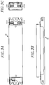
- the LED lighting device of the present embodiment is accommodated in a metal case 90.
- Connectors 121A and 121B are provided at one end side of the case 90 in its longitudinal direction, and are respectively connected to the lamp sockets 120A and 120B.
- a connector 121C is provided at the other end side of the case 90 in its longitudinal direction, and is connected to the commercial AC power supply 100.
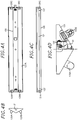
- the LED lighting device accommodated in the case 90 is mounted in, e.g., an illumination apparatus as shown in Figs. 4A to 4D .
- the illumination apparatus includes, e.g., an apparatus body 130 directly attached to the ceiling; and a pair of lamp sockets 120A and 120B serving to supply a power and provided in the apparatus body 130; and a pair of lamp sockets 120C provided in the apparatus body 130 for grounding.
- the apparatus body 130 is made of a metal plate having a substantially rectangular shape in the plan view, and the pair of lamp sockets 120A and 120B for supplying a power and the pair of lamp sockets 120C for grounding are respectively attached to one end side and the other end side of the apparatus body 130 in its longitudinal direction. Further, the LED lighting device accommodated in the case 90 is attached to a lower side of the apparatus body 130. A reflection plate 131 having a substantially triangular shape when viewed in the longitudinal direction of the apparatus body 130 is attached to a lower side of the apparatus body 130. The LED lamps 110A and 110B are arranged under the reflection plate 131.
- the lamp sockets 120A and 120B have the same structure as the lamp sockets of the conventionally straight tubular fluorescent lamp, a DC current may be supplied to its filament when the fluorescent lamp is erroneously mounted to the lamp sockets 120A and 120B.
- the operation of the power converting unit 2 is stopped as described above when the voltage detected by the voltage detector 4B falls below the preset lower limit which is less than the rated voltage. Accordingly, even when the fluorescent lamp is erroneously mounted, an unsafe phenomenon and/or breakdown of the lighting device do not occur, for example. Here, a user cannot recognize whether such erroneous mounting may cause a safe or an unsafe condition. For that reason, the pin bases of the LED lamps 110A and 110B may be made to have electrode shapes that are different from those of the fluorescent lamp to prevent the erroneous mounting, and the lamp sockets 120A, 120B and 120C may be formed conforming to the pin base shape of the LED lamps 110A and 110B.
- the changeover time T1 may be appropriately set in such a way that an unsafe phenomenon does not occur due to aging deterioration of resin materials.
- the lamp abnormality monitoring control is carried out by using the output voltage V o of the power control unit 2 and the lamp voltage V1 applied to one of the LED lamps 110A and 110B.
Landscapes
- Circuit Arrangement For Electric Light Sources In General (AREA)
- Led Devices (AREA)
Claims (5)
- LED Beleuchtungsvorrichtung umfassend:eine Umrichtereinheit (2) zum Ausgeben einer variablen Ausgangsspannung, wobei zwei LED Lampen (110A, 110B) in Reihe zwischen Ausgabeterminals der Umrichtereinheit durch Lampenfassungen (120A, 120B) verbunden sind;einen Stromdetektor (3) zum Erfassen eines Ausgangsstroms von der Umrichtereinheit (2);einen ersten Spannungsdetektor (4A) zum Erfassen der Ausgangsspannung der Umrichtereinheit (2) und zum Erzeugen einer ersten Erfassungsspannung, die der Ausgangsspannung entspricht;einen zweiten Spannungsdetektor (4B) zum Erfassen einer Spannung, die auf eine der zwei LED Lampen (110A, 110B) angewendet wird und zum Erzeugen einer zweiten Erfassungsspannung, die der angewendeten Spannung entspricht; undeine Steuereinheit (5) zum Steuern der Umrichtereinheit (2), um die Ausgangsspannung anzupassen, um dadurch den Ausgangsstrom mit einem Zielwert in Übereinstimmung zu bringen,wobei die Steuereinheit (5) die Umrichtereinheit (2) steuert, um die Ausgangsspannung zu verringern, wenn zumindest eine der zweiten Erfassungsspannung und der Differenzspannung zwischen der ersten und der zweiten Erfassungsspannung nicht in einen vorbestimmten Spannungsbereich fällt, unddadurch gekennzeichnet, dassdie Steuereinheit (5) eine akkumulierte Beleuchtungszeit der LED Lampen zählt, und monoton, mit einer Zunahme der akkumulierten Beleuchtungszeit, eine obere Grenze des Spannungsbereichs absenkt, nachdem die akkumulierte Beleuchtungszeit eine Umschaltzeit erreicht.
- LED Beleuchtungsvorrichtung nach Anspruch 1, bei der die Steuereinheit (5) die akkumulierte Beleuchtungszeit auf Null zurücksetzt, wenn eine Rücksetzbedingung erfüllt ist.
- LED Beleuchtungsvorrichtung nach Anspruch 2, bei der, nachdem die akkumulierte Beleuchtungszeit eine Rücksetzverhinderungszeit erreicht, die größer als die Umschaltzeit ist, die Steuereinheit (5) die akkumulierte Beleuchtungszeit selbst dann nicht zurücksetzt, wenn die Rücksetzbedingung erfüllt ist.
- Beleuchtungsapparat umfassend:die LED Beleuchtungsvorrichtung nach einem der Ansprüche 1 bis 3;zwei Paare von Lampensockel (120A, 120B); undeinen Vorrichtungskörper (130), durch den die LED Beleuchtungsvorrichtung und die Lampensockel (120A, 120B) gehalten werden.
- LED Beleuchtungsvorrichtung nach Anspruch 1, bei der die Umschaltzeit eine Nenn-Lebensdauer der LED Beleuchtungsvorrichtung ist.
Applications Claiming Priority (1)
| Application Number | Priority Date | Filing Date | Title |
|---|---|---|---|
| JP2010292761A JP5760171B2 (ja) | 2010-12-28 | 2010-12-28 | Led点灯装置及びそれを用いた照明器具 |
Publications (3)
| Publication Number | Publication Date |
|---|---|
| EP2473003A2 EP2473003A2 (de) | 2012-07-04 |
| EP2473003A3 EP2473003A3 (de) | 2014-05-14 |
| EP2473003B1 true EP2473003B1 (de) | 2018-10-10 |
Family
ID=45495579
Family Applications (2)
| Application Number | Title | Priority Date | Filing Date |
|---|---|---|---|
| EP11194629.9A Withdrawn EP2473006A3 (de) | 2010-12-28 | 2011-12-20 | LED-Beleuchtungsvorrichtung und Beleuchtungsbefestigung damit |
| EP11010171.4A Not-in-force EP2473003B1 (de) | 2010-12-28 | 2011-12-23 | LED-Lichtvorrichtung und Beleuchtungsvorrichtung damit |
Family Applications Before (1)
| Application Number | Title | Priority Date | Filing Date |
|---|---|---|---|
| EP11194629.9A Withdrawn EP2473006A3 (de) | 2010-12-28 | 2011-12-20 | LED-Beleuchtungsvorrichtung und Beleuchtungsbefestigung damit |
Country Status (4)
| Country | Link |
|---|---|
| US (1) | US8786201B2 (de) |
| EP (2) | EP2473006A3 (de) |
| JP (1) | JP5760171B2 (de) |
| CN (1) | CN102548140B (de) |
Families Citing this family (23)
| Publication number | Priority date | Publication date | Assignee | Title |
|---|---|---|---|---|
| JP5904324B2 (ja) * | 2011-02-25 | 2016-04-13 | 東芝ライテック株式会社 | Ledランプ点灯装置および照明器具 |
| JP5214003B2 (ja) * | 2011-08-12 | 2013-06-19 | シャープ株式会社 | 電源装置及び照明装置 |
| JP6079099B2 (ja) * | 2012-09-27 | 2017-02-15 | 市光工業株式会社 | 故障診断装置及び車両用灯具 |
| JP6062227B2 (ja) * | 2012-11-29 | 2017-01-18 | シャープ株式会社 | 電源装置 |
| JP2014108018A (ja) * | 2012-11-29 | 2014-06-09 | Sharp Corp | 電源装置 |
| JP5988214B2 (ja) | 2012-12-04 | 2016-09-07 | パナソニックIpマネジメント株式会社 | 点灯装置およびそれを用いた照明器具 |
| US9565782B2 (en) | 2013-02-15 | 2017-02-07 | Ecosense Lighting Inc. | Field replaceable power supply cartridge |
| DE102013216153A1 (de) | 2013-08-14 | 2015-02-19 | Osram Gmbh | Elektronisches Vorschaltgerät zum Betreiben mindestens einer ersten und einer zweiten Kaskade von LEDs |
| US10477636B1 (en) | 2014-10-28 | 2019-11-12 | Ecosense Lighting Inc. | Lighting systems having multiple light sources |
| CN104507215B (zh) * | 2014-12-04 | 2018-05-04 | 苏州工业园区海的机电科技有限公司 | Led模组点亮检测装置及其点亮检测方法 |
| US11306897B2 (en) | 2015-02-09 | 2022-04-19 | Ecosense Lighting Inc. | Lighting systems generating partially-collimated light emissions |
| US9869450B2 (en) | 2015-02-09 | 2018-01-16 | Ecosense Lighting Inc. | Lighting systems having a truncated parabolic- or hyperbolic-conical light reflector, or a total internal reflection lens; and having another light reflector |
| US9568665B2 (en) | 2015-03-03 | 2017-02-14 | Ecosense Lighting Inc. | Lighting systems including lens modules for selectable light distribution |
| US9746159B1 (en) | 2015-03-03 | 2017-08-29 | Ecosense Lighting Inc. | Lighting system having a sealing system |
| US9651216B2 (en) | 2015-03-03 | 2017-05-16 | Ecosense Lighting Inc. | Lighting systems including asymmetric lens modules for selectable light distribution |
| US9651227B2 (en) | 2015-03-03 | 2017-05-16 | Ecosense Lighting Inc. | Low-profile lighting system having pivotable lighting enclosure |
| USD785218S1 (en) | 2015-07-06 | 2017-04-25 | Ecosense Lighting Inc. | LED luminaire having a mounting system |
| USD782094S1 (en) | 2015-07-20 | 2017-03-21 | Ecosense Lighting Inc. | LED luminaire having a mounting system |
| USD782093S1 (en) | 2015-07-20 | 2017-03-21 | Ecosense Lighting Inc. | LED luminaire having a mounting system |
| US9651232B1 (en) | 2015-08-03 | 2017-05-16 | Ecosense Lighting Inc. | Lighting system having a mounting device |
| DE102018122067A1 (de) * | 2018-09-11 | 2020-03-12 | HELLA GmbH & Co. KGaA | LED-Leuchtvorrichtung mit Fehlerdetektion und Kraftfahrzeug |
| JP7278171B2 (ja) * | 2019-08-08 | 2023-05-19 | シーシーエス株式会社 | Led玉切れ検知機構及びこれを用いたled光照射システム |
| KR102217889B1 (ko) * | 2020-05-26 | 2021-02-19 | 박영기 | 누계전류량 특이값 검출 기반의 led디지털사이니지 불량감지시스템 |
Citations (1)
| Publication number | Priority date | Publication date | Assignee | Title |
|---|---|---|---|---|
| JP2006210272A (ja) * | 2005-01-31 | 2006-08-10 | Matsushita Electric Works Ltd | Led駆動装置、及びそれを用いた照明装置 |
Family Cites Families (16)
| Publication number | Priority date | Publication date | Assignee | Title |
|---|---|---|---|---|
| DE19734750C2 (de) | 1997-08-12 | 2003-04-30 | Reitter & Schefenacker Gmbh | Heckleuchte von Kraftfahrzeugen |
| JP4500172B2 (ja) * | 2005-01-31 | 2010-07-14 | パナソニック電工株式会社 | Led駆動装置、照明装置、照明器具 |
| JP4169008B2 (ja) | 2005-01-31 | 2008-10-22 | 松下電工株式会社 | Led駆動装置、及びそれを用いた照明装置 |
| JP2006210219A (ja) | 2005-01-31 | 2006-08-10 | Koito Mfg Co Ltd | 車両用灯具の点灯制御回路 |
| JP5085033B2 (ja) | 2005-12-12 | 2012-11-28 | 株式会社小糸製作所 | 車両用発光装置 |
| US7800876B2 (en) * | 2006-01-09 | 2010-09-21 | Microsemi Corp. - Analog Mixed Signal Group Ltd. | Fault detection mechanism for LED backlighting |
| US8111014B2 (en) | 2006-06-26 | 2012-02-07 | Koninklijke Philips Electronics N.V. | Drive circuit for driving a load with constant current |
| JP2008210271A (ja) | 2007-02-27 | 2008-09-11 | Kujirai Media Create:Kk | 記憶媒体製造方法、および情報処理システム |
| JP5142620B2 (ja) | 2007-08-06 | 2013-02-13 | シャープ株式会社 | 照明装置 |
| JP2009111035A (ja) | 2007-10-26 | 2009-05-21 | Panasonic Electric Works Co Ltd | 発光ダイオード駆動装置、発光ダイオード駆動装置を用いた照明装置、車室内用照明装置、車両用照明装置 |
| CN101534594A (zh) | 2008-03-12 | 2009-09-16 | 奇美电子股份有限公司 | 发光二极管串列的短路保护电路及其方法 |
| JP2009302296A (ja) * | 2008-06-13 | 2009-12-24 | Panasonic Electric Works Co Ltd | 発光ダイオード駆動装置並びにそれを用いた照明器具、車室内用照明装置、車両用照明装置 |
| JP2010113897A (ja) * | 2008-11-05 | 2010-05-20 | Panasonic Corp | 照明装置 |
| US8466619B2 (en) * | 2008-11-11 | 2013-06-18 | Dongbu Hitek Co., Ltd. | Illumination apparatus and driving method thereof |
| US8044667B2 (en) | 2009-04-20 | 2011-10-25 | Infineon Technologies Ag | Failure detection for series of electrical loads |
| TWI388115B (zh) * | 2009-08-13 | 2013-03-01 | Green Solution Tech Co Ltd | 電源轉換驅動電路及螢光燈管驅動電路 |
-
2010
- 2010-12-28 JP JP2010292761A patent/JP5760171B2/ja active Active
-
2011
- 2011-12-15 US US13/326,386 patent/US8786201B2/en not_active Expired - Fee Related
- 2011-12-20 EP EP11194629.9A patent/EP2473006A3/de not_active Withdrawn
- 2011-12-23 EP EP11010171.4A patent/EP2473003B1/de not_active Not-in-force
- 2011-12-26 CN CN201110441266.6A patent/CN102548140B/zh not_active Expired - Fee Related
Patent Citations (1)
| Publication number | Priority date | Publication date | Assignee | Title |
|---|---|---|---|---|
| JP2006210272A (ja) * | 2005-01-31 | 2006-08-10 | Matsushita Electric Works Ltd | Led駆動装置、及びそれを用いた照明装置 |
Also Published As
| Publication number | Publication date |
|---|---|
| US8786201B2 (en) | 2014-07-22 |
| JP5760171B2 (ja) | 2015-08-05 |
| EP2473006A3 (de) | 2014-05-14 |
| CN102548140A (zh) | 2012-07-04 |
| EP2473003A3 (de) | 2014-05-14 |
| JP2012142358A (ja) | 2012-07-26 |
| EP2473006A2 (de) | 2012-07-04 |
| EP2473003A2 (de) | 2012-07-04 |
| US20120161649A1 (en) | 2012-06-28 |
| CN102548140B (zh) | 2014-08-27 |
Similar Documents
| Publication | Publication Date | Title |
|---|---|---|
| EP2473003B1 (de) | LED-Lichtvorrichtung und Beleuchtungsvorrichtung damit | |
| JP5828103B2 (ja) | Led点灯装置及びそれを用いた照明器具 | |
| US8581512B2 (en) | Light source module, lighting apparatus, and illumination device using the same | |
| US8564210B2 (en) | Light source module and lighting apparatus, and illumination apparatus using same | |
| CN102651938B (zh) | 点灯装置以及照明装置 | |
| JP5379921B2 (ja) | Led点灯装置及びそれを用いた照明器具 | |
| JP5480668B2 (ja) | 光源モジュール、点灯装置およびそれを用いた照明器具 | |
| US20120194075A1 (en) | Lighting device and luminaire | |
| JP2012009391A (ja) | Led点灯装置 | |
| JPWO2020045271A1 (ja) | 点灯回路および車両用灯具 | |
| JP5525393B2 (ja) | Led点灯装置及びそれを用いた照明器具 | |
| US9320106B2 (en) | Lighting device and luminaire using the same | |
| JP5645250B2 (ja) | Led点灯装置及びそれを用いた照明器具 | |
| CN102316638B (zh) | Led点灯装置及使用了该led点灯装置的照明器具 |
Legal Events
| Date | Code | Title | Description |
|---|---|---|---|
| AK | Designated contracting states |
Kind code of ref document: A2 Designated state(s): AL AT BE BG CH CY CZ DE DK EE ES FI FR GB GR HR HU IE IS IT LI LT LU LV MC MK MT NL NO PL PT RO RS SE SI SK SM TR |
|
| AX | Request for extension of the european patent |
Extension state: BA ME |
|
| PUAI | Public reference made under article 153(3) epc to a published international application that has entered the european phase |
Free format text: ORIGINAL CODE: 0009012 |
|
| RAP1 | Party data changed (applicant data changed or rights of an application transferred) |
Owner name: PANASONIC CORPORATION |
|
| PUAL | Search report despatched |
Free format text: ORIGINAL CODE: 0009013 |
|
| 17P | Request for examination filed |
Effective date: 20140331 |
|
| AK | Designated contracting states |
Kind code of ref document: A3 Designated state(s): AL AT BE BG CH CY CZ DE DK EE ES FI FR GB GR HR HU IE IS IT LI LT LU LV MC MK MT NL NO PL PT RO RS SE SI SK SM TR |
|
| AX | Request for extension of the european patent |
Extension state: BA ME |
|
| RBV | Designated contracting states (corrected) |
Designated state(s): AL AT BE BG CH CY CZ DE DK EE ES FI FR GB GR HR HU IE IS IT LI LT LU LV MC MK MT NL NO PL PT RO RS SE SI SK SM TR |
|
| RIC1 | Information provided on ipc code assigned before grant |
Ipc: H05B 33/08 20060101AFI20140410BHEP |
|
| RAP1 | Party data changed (applicant data changed or rights of an application transferred) |
Owner name: PANASONIC INTELLECTUAL PROPERTY MANAGEMENT CO., LT |
|
| GRAP | Despatch of communication of intention to grant a patent |
Free format text: ORIGINAL CODE: EPIDOSNIGR1 |
|
| INTG | Intention to grant announced |
Effective date: 20170911 |
|
| GRAS | Grant fee paid |
Free format text: ORIGINAL CODE: EPIDOSNIGR3 |
|
| GRAJ | Information related to disapproval of communication of intention to grant by the applicant or resumption of examination proceedings by the epo deleted |
Free format text: ORIGINAL CODE: EPIDOSDIGR1 |
|
| GRAL | Information related to payment of fee for publishing/printing deleted |
Free format text: ORIGINAL CODE: EPIDOSDIGR3 |
|
| INTC | Intention to grant announced (deleted) | ||
| GRAP | Despatch of communication of intention to grant a patent |
Free format text: ORIGINAL CODE: EPIDOSNIGR1 |
|
| INTG | Intention to grant announced |
Effective date: 20180419 |
|
| GRAA | (expected) grant |
Free format text: ORIGINAL CODE: 0009210 |
|
| AK | Designated contracting states |
Kind code of ref document: B1 Designated state(s): AL AT BE BG CH CY CZ DE DK EE ES FI FR GB GR HR HU IE IS IT LI LT LU LV MC MK MT NL NO PL PT RO RS SE SI SK SM TR |
|
| REG | Reference to a national code |
Ref country code: GB Ref legal event code: FG4D |
|
| REG | Reference to a national code |
Ref country code: CH Ref legal event code: EP Ref country code: AT Ref legal event code: REF Ref document number: 1052807 Country of ref document: AT Kind code of ref document: T Effective date: 20181015 |
|
| REG | Reference to a national code |
Ref country code: IE Ref legal event code: FG4D |
|
| REG | Reference to a national code |
Ref country code: DE Ref legal event code: R096 Ref document number: 602011052696 Country of ref document: DE |
|
| REG | Reference to a national code |
Ref country code: NL Ref legal event code: MP Effective date: 20181010 |
|
| REG | Reference to a national code |
Ref country code: LT Ref legal event code: MG4D |
|
| REG | Reference to a national code |
Ref country code: AT Ref legal event code: MK05 Ref document number: 1052807 Country of ref document: AT Kind code of ref document: T Effective date: 20181010 |
|
| PG25 | Lapsed in a contracting state [announced via postgrant information from national office to epo] |
Ref country code: NL Free format text: LAPSE BECAUSE OF FAILURE TO SUBMIT A TRANSLATION OF THE DESCRIPTION OR TO PAY THE FEE WITHIN THE PRESCRIBED TIME-LIMIT Effective date: 20181010 |
|
| PG25 | Lapsed in a contracting state [announced via postgrant information from national office to epo] |
Ref country code: NO Free format text: LAPSE BECAUSE OF FAILURE TO SUBMIT A TRANSLATION OF THE DESCRIPTION OR TO PAY THE FEE WITHIN THE PRESCRIBED TIME-LIMIT Effective date: 20190110 Ref country code: LV Free format text: LAPSE BECAUSE OF FAILURE TO SUBMIT A TRANSLATION OF THE DESCRIPTION OR TO PAY THE FEE WITHIN THE PRESCRIBED TIME-LIMIT Effective date: 20181010 Ref country code: LT Free format text: LAPSE BECAUSE OF FAILURE TO SUBMIT A TRANSLATION OF THE DESCRIPTION OR TO PAY THE FEE WITHIN THE PRESCRIBED TIME-LIMIT Effective date: 20181010 Ref country code: IS Free format text: LAPSE BECAUSE OF FAILURE TO SUBMIT A TRANSLATION OF THE DESCRIPTION OR TO PAY THE FEE WITHIN THE PRESCRIBED TIME-LIMIT Effective date: 20190210 Ref country code: AT Free format text: LAPSE BECAUSE OF FAILURE TO SUBMIT A TRANSLATION OF THE DESCRIPTION OR TO PAY THE FEE WITHIN THE PRESCRIBED TIME-LIMIT Effective date: 20181010 Ref country code: FI Free format text: LAPSE BECAUSE OF FAILURE TO SUBMIT A TRANSLATION OF THE DESCRIPTION OR TO PAY THE FEE WITHIN THE PRESCRIBED TIME-LIMIT Effective date: 20181010 Ref country code: ES Free format text: LAPSE BECAUSE OF FAILURE TO SUBMIT A TRANSLATION OF THE DESCRIPTION OR TO PAY THE FEE WITHIN THE PRESCRIBED TIME-LIMIT Effective date: 20181010 Ref country code: BG Free format text: LAPSE BECAUSE OF FAILURE TO SUBMIT A TRANSLATION OF THE DESCRIPTION OR TO PAY THE FEE WITHIN THE PRESCRIBED TIME-LIMIT Effective date: 20190110 Ref country code: PL Free format text: LAPSE BECAUSE OF FAILURE TO SUBMIT A TRANSLATION OF THE DESCRIPTION OR TO PAY THE FEE WITHIN THE PRESCRIBED TIME-LIMIT Effective date: 20181010 Ref country code: HR Free format text: LAPSE BECAUSE OF FAILURE TO SUBMIT A TRANSLATION OF THE DESCRIPTION OR TO PAY THE FEE WITHIN THE PRESCRIBED TIME-LIMIT Effective date: 20181010 |
|
| PG25 | Lapsed in a contracting state [announced via postgrant information from national office to epo] |
Ref country code: SE Free format text: LAPSE BECAUSE OF FAILURE TO SUBMIT A TRANSLATION OF THE DESCRIPTION OR TO PAY THE FEE WITHIN THE PRESCRIBED TIME-LIMIT Effective date: 20181010 Ref country code: AL Free format text: LAPSE BECAUSE OF FAILURE TO SUBMIT A TRANSLATION OF THE DESCRIPTION OR TO PAY THE FEE WITHIN THE PRESCRIBED TIME-LIMIT Effective date: 20181010 Ref country code: PT Free format text: LAPSE BECAUSE OF FAILURE TO SUBMIT A TRANSLATION OF THE DESCRIPTION OR TO PAY THE FEE WITHIN THE PRESCRIBED TIME-LIMIT Effective date: 20190210 Ref country code: RS Free format text: LAPSE BECAUSE OF FAILURE TO SUBMIT A TRANSLATION OF THE DESCRIPTION OR TO PAY THE FEE WITHIN THE PRESCRIBED TIME-LIMIT Effective date: 20181010 Ref country code: GR Free format text: LAPSE BECAUSE OF FAILURE TO SUBMIT A TRANSLATION OF THE DESCRIPTION OR TO PAY THE FEE WITHIN THE PRESCRIBED TIME-LIMIT Effective date: 20190111 |
|
| REG | Reference to a national code |
Ref country code: DE Ref legal event code: R097 Ref document number: 602011052696 Country of ref document: DE |
|
| PG25 | Lapsed in a contracting state [announced via postgrant information from national office to epo] |
Ref country code: DK Free format text: LAPSE BECAUSE OF FAILURE TO SUBMIT A TRANSLATION OF THE DESCRIPTION OR TO PAY THE FEE WITHIN THE PRESCRIBED TIME-LIMIT Effective date: 20181010 Ref country code: CZ Free format text: LAPSE BECAUSE OF FAILURE TO SUBMIT A TRANSLATION OF THE DESCRIPTION OR TO PAY THE FEE WITHIN THE PRESCRIBED TIME-LIMIT Effective date: 20181010 Ref country code: IT Free format text: LAPSE BECAUSE OF FAILURE TO SUBMIT A TRANSLATION OF THE DESCRIPTION OR TO PAY THE FEE WITHIN THE PRESCRIBED TIME-LIMIT Effective date: 20181010 |
|
| REG | Reference to a national code |
Ref country code: CH Ref legal event code: PL |
|
| PLBE | No opposition filed within time limit |
Free format text: ORIGINAL CODE: 0009261 |
|
| STAA | Information on the status of an ep patent application or granted ep patent |
Free format text: STATUS: NO OPPOSITION FILED WITHIN TIME LIMIT |
|
| PG25 | Lapsed in a contracting state [announced via postgrant information from national office to epo] |
Ref country code: RO Free format text: LAPSE BECAUSE OF FAILURE TO SUBMIT A TRANSLATION OF THE DESCRIPTION OR TO PAY THE FEE WITHIN THE PRESCRIBED TIME-LIMIT Effective date: 20181010 Ref country code: EE Free format text: LAPSE BECAUSE OF FAILURE TO SUBMIT A TRANSLATION OF THE DESCRIPTION OR TO PAY THE FEE WITHIN THE PRESCRIBED TIME-LIMIT Effective date: 20181010 Ref country code: SM Free format text: LAPSE BECAUSE OF FAILURE TO SUBMIT A TRANSLATION OF THE DESCRIPTION OR TO PAY THE FEE WITHIN THE PRESCRIBED TIME-LIMIT Effective date: 20181010 Ref country code: LU Free format text: LAPSE BECAUSE OF NON-PAYMENT OF DUE FEES Effective date: 20181223 Ref country code: SK Free format text: LAPSE BECAUSE OF FAILURE TO SUBMIT A TRANSLATION OF THE DESCRIPTION OR TO PAY THE FEE WITHIN THE PRESCRIBED TIME-LIMIT Effective date: 20181010 Ref country code: MC Free format text: LAPSE BECAUSE OF FAILURE TO SUBMIT A TRANSLATION OF THE DESCRIPTION OR TO PAY THE FEE WITHIN THE PRESCRIBED TIME-LIMIT Effective date: 20181010 |
|
| 26N | No opposition filed |
Effective date: 20190711 |
|
| REG | Reference to a national code |
Ref country code: IE Ref legal event code: MM4A |
|
| GBPC | Gb: european patent ceased through non-payment of renewal fee |
Effective date: 20190110 |
|
| REG | Reference to a national code |
Ref country code: BE Ref legal event code: MM Effective date: 20181231 |
|
| PG25 | Lapsed in a contracting state [announced via postgrant information from national office to epo] |
Ref country code: FR Free format text: LAPSE BECAUSE OF NON-PAYMENT OF DUE FEES Effective date: 20181231 Ref country code: IE Free format text: LAPSE BECAUSE OF NON-PAYMENT OF DUE FEES Effective date: 20181223 Ref country code: SI Free format text: LAPSE BECAUSE OF FAILURE TO SUBMIT A TRANSLATION OF THE DESCRIPTION OR TO PAY THE FEE WITHIN THE PRESCRIBED TIME-LIMIT Effective date: 20181010 |
|
| REG | Reference to a national code |
Ref country code: DE Ref legal event code: R079 Ref document number: 602011052696 Country of ref document: DE Free format text: PREVIOUS MAIN CLASS: H05B0033080000 Ipc: H05B0045000000 |
|
| PG25 | Lapsed in a contracting state [announced via postgrant information from national office to epo] |
Ref country code: BE Free format text: LAPSE BECAUSE OF NON-PAYMENT OF DUE FEES Effective date: 20181231 |
|
| PG25 | Lapsed in a contracting state [announced via postgrant information from national office to epo] |
Ref country code: CH Free format text: LAPSE BECAUSE OF NON-PAYMENT OF DUE FEES Effective date: 20181231 Ref country code: LI Free format text: LAPSE BECAUSE OF NON-PAYMENT OF DUE FEES Effective date: 20181231 Ref country code: GB Free format text: LAPSE BECAUSE OF NON-PAYMENT OF DUE FEES Effective date: 20190110 |
|
| PG25 | Lapsed in a contracting state [announced via postgrant information from national office to epo] |
Ref country code: MT Free format text: LAPSE BECAUSE OF NON-PAYMENT OF DUE FEES Effective date: 20181223 |
|
| PGFP | Annual fee paid to national office [announced via postgrant information from national office to epo] |
Ref country code: DE Payment date: 20191210 Year of fee payment: 9 |
|
| PG25 | Lapsed in a contracting state [announced via postgrant information from national office to epo] |
Ref country code: TR Free format text: LAPSE BECAUSE OF FAILURE TO SUBMIT A TRANSLATION OF THE DESCRIPTION OR TO PAY THE FEE WITHIN THE PRESCRIBED TIME-LIMIT Effective date: 20181010 |
|
| PG25 | Lapsed in a contracting state [announced via postgrant information from national office to epo] |
Ref country code: HU Free format text: LAPSE BECAUSE OF FAILURE TO SUBMIT A TRANSLATION OF THE DESCRIPTION OR TO PAY THE FEE WITHIN THE PRESCRIBED TIME-LIMIT; INVALID AB INITIO Effective date: 20111223 Ref country code: MK Free format text: LAPSE BECAUSE OF NON-PAYMENT OF DUE FEES Effective date: 20181010 Ref country code: CY Free format text: LAPSE BECAUSE OF FAILURE TO SUBMIT A TRANSLATION OF THE DESCRIPTION OR TO PAY THE FEE WITHIN THE PRESCRIBED TIME-LIMIT Effective date: 20181010 |
|
| REG | Reference to a national code |
Ref country code: DE Ref legal event code: R119 Ref document number: 602011052696 Country of ref document: DE |
|
| PG25 | Lapsed in a contracting state [announced via postgrant information from national office to epo] |
Ref country code: DE Free format text: LAPSE BECAUSE OF NON-PAYMENT OF DUE FEES Effective date: 20210701 |