EP2474209B1 - Procédé permettant de connecter plusieurs éléments d'une carte de circuit imprimé, carte de circuit imprimé et utilisation d'un tel procédé - Google Patents
Procédé permettant de connecter plusieurs éléments d'une carte de circuit imprimé, carte de circuit imprimé et utilisation d'un tel procédé Download PDFInfo
- Publication number
- EP2474209B1 EP2474209B1 EP10755076.6A EP10755076A EP2474209B1 EP 2474209 B1 EP2474209 B1 EP 2474209B1 EP 10755076 A EP10755076 A EP 10755076A EP 2474209 B1 EP2474209 B1 EP 2474209B1
- Authority
- EP
- European Patent Office
- Prior art keywords
- elements
- circuit board
- printed circuit
- peripheral regions
- adhesive
- Prior art date
- Legal status (The legal status is an assumption and is not a legal conclusion. Google has not performed a legal analysis and makes no representation as to the accuracy of the status listed.)
- Active
Links
Images



Classifications
-
- H—ELECTRICITY
- H05—ELECTRIC TECHNIQUES NOT OTHERWISE PROVIDED FOR
- H05K—PRINTED CIRCUITS; CASINGS OR CONSTRUCTIONAL DETAILS OF ELECTRIC APPARATUS; MANUFACTURE OF ASSEMBLAGES OF ELECTRICAL COMPONENTS
- H05K3/00—Apparatus or processes for manufacturing printed circuits
- H05K3/30—Assembling printed circuits with electric components, e.g. with resistors
- H05K3/303—Assembling printed circuits with electric components, e.g. with resistors with surface mounted components
- H05K3/305—Affixing by adhesive
-
- H—ELECTRICITY
- H05—ELECTRIC TECHNIQUES NOT OTHERWISE PROVIDED FOR
- H05K—PRINTED CIRCUITS; CASINGS OR CONSTRUCTIONAL DETAILS OF ELECTRIC APPARATUS; MANUFACTURE OF ASSEMBLAGES OF ELECTRICAL COMPONENTS
- H05K1/00—Printed circuits
- H05K1/02—Details
- H05K1/14—Structural association of two or more printed circuits
- H05K1/142—Arrangements of planar printed circuit boards in the same plane, e.g. auxiliary printed circuit insert mounted in a main printed circuit
-
- H—ELECTRICITY
- H05—ELECTRIC TECHNIQUES NOT OTHERWISE PROVIDED FOR
- H05K—PRINTED CIRCUITS; CASINGS OR CONSTRUCTIONAL DETAILS OF ELECTRIC APPARATUS; MANUFACTURE OF ASSEMBLAGES OF ELECTRICAL COMPONENTS
- H05K1/00—Printed circuits
- H05K1/18—Printed circuits structurally associated with non-printed electric components
- H05K1/181—Printed circuits structurally associated with non-printed electric components associated with surface mounted components
-
- H—ELECTRICITY
- H05—ELECTRIC TECHNIQUES NOT OTHERWISE PROVIDED FOR
- H05K—PRINTED CIRCUITS; CASINGS OR CONSTRUCTIONAL DETAILS OF ELECTRIC APPARATUS; MANUFACTURE OF ASSEMBLAGES OF ELECTRICAL COMPONENTS
- H05K3/00—Apparatus or processes for manufacturing printed circuits
- H05K3/0097—Processing two or more printed circuits simultaneously, e.g. made from a common substrate, or temporarily stacked circuit boards
-
- H—ELECTRICITY
- H05—ELECTRIC TECHNIQUES NOT OTHERWISE PROVIDED FOR
- H05K—PRINTED CIRCUITS; CASINGS OR CONSTRUCTIONAL DETAILS OF ELECTRIC APPARATUS; MANUFACTURE OF ASSEMBLAGES OF ELECTRICAL COMPONENTS
- H05K1/00—Printed circuits
- H05K1/02—Details
- H05K1/0266—Marks, test patterns or identification means
- H05K1/0269—Marks, test patterns or identification means for visual or optical inspection
-
- H—ELECTRICITY
- H05—ELECTRIC TECHNIQUES NOT OTHERWISE PROVIDED FOR
- H05K—PRINTED CIRCUITS; CASINGS OR CONSTRUCTIONAL DETAILS OF ELECTRIC APPARATUS; MANUFACTURE OF ASSEMBLAGES OF ELECTRICAL COMPONENTS
- H05K2201/00—Indexing scheme relating to printed circuits covered by H05K1/00
- H05K2201/09—Shape and layout
- H05K2201/09009—Substrate related
- H05K2201/09063—Holes or slots in insulating substrate not used for electrical connections
-
- H—ELECTRICITY
- H05—ELECTRIC TECHNIQUES NOT OTHERWISE PROVIDED FOR
- H05K—PRINTED CIRCUITS; CASINGS OR CONSTRUCTIONAL DETAILS OF ELECTRIC APPARATUS; MANUFACTURE OF ASSEMBLAGES OF ELECTRICAL COMPONENTS
- H05K2201/00—Indexing scheme relating to printed circuits covered by H05K1/00
- H05K2201/09—Shape and layout
- H05K2201/09145—Edge details
-
- H—ELECTRICITY
- H05—ELECTRIC TECHNIQUES NOT OTHERWISE PROVIDED FOR
- H05K—PRINTED CIRCUITS; CASINGS OR CONSTRUCTIONAL DETAILS OF ELECTRIC APPARATUS; MANUFACTURE OF ASSEMBLAGES OF ELECTRICAL COMPONENTS
- H05K2201/00—Indexing scheme relating to printed circuits covered by H05K1/00
- H05K2201/09—Shape and layout
- H05K2201/09818—Shape or layout details not covered by a single group of H05K2201/09009 - H05K2201/09809
- H05K2201/09918—Optically detected marks used for aligning tool relative to the PCB, e.g. for mounting of components
-
- H—ELECTRICITY
- H05—ELECTRIC TECHNIQUES NOT OTHERWISE PROVIDED FOR
- H05K—PRINTED CIRCUITS; CASINGS OR CONSTRUCTIONAL DETAILS OF ELECTRIC APPARATUS; MANUFACTURE OF ASSEMBLAGES OF ELECTRICAL COMPONENTS
- H05K2201/00—Indexing scheme relating to printed circuits covered by H05K1/00
- H05K2201/10—Details of components or other objects attached to or integrated in a printed circuit board
- H05K2201/10431—Details of mounted components
- H05K2201/10598—Means for fastening a component, a casing or a heat sink whereby a pressure is exerted on the component towards the PCB
-
- H—ELECTRICITY
- H05—ELECTRIC TECHNIQUES NOT OTHERWISE PROVIDED FOR
- H05K—PRINTED CIRCUITS; CASINGS OR CONSTRUCTIONAL DETAILS OF ELECTRIC APPARATUS; MANUFACTURE OF ASSEMBLAGES OF ELECTRICAL COMPONENTS
- H05K2203/00—Indexing scheme relating to apparatus or processes for manufacturing printed circuits covered by H05K3/00
- H05K2203/01—Tools for processing; Objects used during processing
- H05K2203/0147—Carriers and holders
- H05K2203/0169—Using a temporary frame during processing
-
- H—ELECTRICITY
- H05—ELECTRIC TECHNIQUES NOT OTHERWISE PROVIDED FOR
- H05K—PRINTED CIRCUITS; CASINGS OR CONSTRUCTIONAL DETAILS OF ELECTRIC APPARATUS; MANUFACTURE OF ASSEMBLAGES OF ELECTRICAL COMPONENTS
- H05K2203/00—Indexing scheme relating to apparatus or processes for manufacturing printed circuits covered by H05K3/00
- H05K2203/16—Inspection; Monitoring; Aligning
- H05K2203/167—Using mechanical means for positioning, alignment or registration, e.g. using rod-in-hole alignment
-
- Y—GENERAL TAGGING OF NEW TECHNOLOGICAL DEVELOPMENTS; GENERAL TAGGING OF CROSS-SECTIONAL TECHNOLOGIES SPANNING OVER SEVERAL SECTIONS OF THE IPC; TECHNICAL SUBJECTS COVERED BY FORMER USPC CROSS-REFERENCE ART COLLECTIONS [XRACs] AND DIGESTS
- Y10—TECHNICAL SUBJECTS COVERED BY FORMER USPC
- Y10T—TECHNICAL SUBJECTS COVERED BY FORMER US CLASSIFICATION
- Y10T156/00—Adhesive bonding and miscellaneous chemical manufacture
- Y10T156/10—Methods of surface bonding and/or assembly therefor
- Y10T156/1089—Methods of surface bonding and/or assembly therefor of discrete laminae to single face of additional lamina
-
- Y—GENERAL TAGGING OF NEW TECHNOLOGICAL DEVELOPMENTS; GENERAL TAGGING OF CROSS-SECTIONAL TECHNOLOGIES SPANNING OVER SEVERAL SECTIONS OF THE IPC; TECHNICAL SUBJECTS COVERED BY FORMER USPC CROSS-REFERENCE ART COLLECTIONS [XRACs] AND DIGESTS
- Y10—TECHNICAL SUBJECTS COVERED BY FORMER USPC
- Y10T—TECHNICAL SUBJECTS COVERED BY FORMER US CLASSIFICATION
- Y10T29/00—Metal working
- Y10T29/49—Method of mechanical manufacture
- Y10T29/49002—Electrical device making
- Y10T29/49117—Conductor or circuit manufacturing
-
- Y—GENERAL TAGGING OF NEW TECHNOLOGICAL DEVELOPMENTS; GENERAL TAGGING OF CROSS-SECTIONAL TECHNOLOGIES SPANNING OVER SEVERAL SECTIONS OF THE IPC; TECHNICAL SUBJECTS COVERED BY FORMER USPC CROSS-REFERENCE ART COLLECTIONS [XRACs] AND DIGESTS
- Y10—TECHNICAL SUBJECTS COVERED BY FORMER USPC
- Y10T—TECHNICAL SUBJECTS COVERED BY FORMER US CLASSIFICATION
- Y10T29/00—Metal working
- Y10T29/49—Method of mechanical manufacture
- Y10T29/49002—Electrical device making
- Y10T29/49117—Conductor or circuit manufacturing
- Y10T29/49124—On flat or curved insulated base, e.g., printed circuit, etc.
- Y10T29/4913—Assembling to base an electrical component, e.g., capacitor, etc.
-
- Y—GENERAL TAGGING OF NEW TECHNOLOGICAL DEVELOPMENTS; GENERAL TAGGING OF CROSS-SECTIONAL TECHNOLOGIES SPANNING OVER SEVERAL SECTIONS OF THE IPC; TECHNICAL SUBJECTS COVERED BY FORMER USPC CROSS-REFERENCE ART COLLECTIONS [XRACs] AND DIGESTS
- Y10—TECHNICAL SUBJECTS COVERED BY FORMER USPC
- Y10T—TECHNICAL SUBJECTS COVERED BY FORMER US CLASSIFICATION
- Y10T29/00—Metal working
- Y10T29/49—Method of mechanical manufacture
- Y10T29/49002—Electrical device making
- Y10T29/49117—Conductor or circuit manufacturing
- Y10T29/49124—On flat or curved insulated base, e.g., printed circuit, etc.
- Y10T29/4913—Assembling to base an electrical component, e.g., capacitor, etc.
- Y10T29/49144—Assembling to base an electrical component, e.g., capacitor, etc. by metal fusion
Definitions
- the invention further relates to a printed circuit board, which consists of a plurality of interconnected elements, wherein at least two elements of the printed circuit board to be connected to each other at least a peripheral region of the same mechanically adhering to each other while adhering to a distance and supported on a support member by bonding, characterized in that the distance between the mutually facing and interconnected peripheral regions is selected with a maximum of 500 microns, in particular a maximum of 200 microns, and to a use of such a method for producing a multi-part circuit board.
- This edge region is provided, for example, to perform further processing steps of such a printed circuit board, such as in the context of equipping with at least one surface to be determined components and / or installation in an electrical or electronic device to a handling and in particular an automatic gripping such a circuit board to allow in the context of subsequent processing or processing steps.
- the peripheral region available for the frame or edge region of the printed circuit board is likewise produced from usually costly material in accordance with the usually multilayer printed circuit board.
- a peripheral area which is not required for the function of the circuit board in view of a usually multi-layered construction of costly materials, but leads to increased costs of such a circuit board.
- manufacturing methods of printed circuit boards lying between individual PCB elements areas or areas of the common plate-like element discarded as waste so that in this context increased costs for the production of printed circuit boards or PCB elements accrue.
- a disadvantage of these known methods for inserting printed circuit boards in a circuit board completely surrounding each frame member is in particular the fact that adapted for the arrangement and interference fit of the circuit boards in the frame member receiving openings adapted exactly to the dimensions and shapes of the printed circuit boards to be used while maintaining low manufacturing tolerances must be and thus a proper positioning and fixing, for example by means of a bond to the peripheral edges of the usually a comparatively small thickness having printed circuit boards and frame elements is extremely difficult and expensive.
- a method and a printed circuit board of the type mentioned above are also the US 2002/0152609 A1 to be taken, with particular reference to the replacement of defective circuit boards.
- the invention aims to prevent or minimize the problems of known embodiments, in particular in connection with a precise connection of a plurality of circuit board elements.
- the present invention aims to provide a method and a printed circuit board of the type mentioned above, in which a compound of at least two elements simplified to a common circuit board and avoiding tight or accurate manufacturing tolerances can conveniently be made largely automated.
- a method for connecting a plurality of elements of a printed circuit board of the type mentioned above essentially characterized in that the distance between the mutually facing and interconnected peripheral regions with a maximum of 500 microns, especially a maximum of 200 microns is selected.
- the circuit board elements to be connected to one another be connected to the carrier element during the connection process by applying a vacuum, by clamping, be kept secured by an entry of protruding from the support member surveys or pins in complementary recesses of the elements or the like.
- the invention proposes alternatively or additionally that the surface of the support element directed to the elements to be supported from a slipping material, such as silicone, rubber or the like. Formed or coated with it.
- the distance between the mutually facing and interconnected peripheral regions with a maximum of 500 microns, In particular, a maximum of 200 microns is selected.
- elements to be connected to one another are arranged and connected to one another with reference to at least one registration element arranged on one of the elements to be connected to one another.
- Such an alignment or registration element can be formed, for example, by an opening or opening on at least one of elements to be connected to one another.
- processing or processing of a plurality of optionally each consisting of several elements printed circuit boards It is also known to provide a corresponding plurality of alignment or positioning elements in such panel-like arrangements of a plurality of circuit boards so as to enable reliable positioning of a plurality of elements.
- a thermal curing of the adhesive at a temperature between 80 ° C and 300 ° C.
- a high-viscosity adhesive be used.
- Such an adhesive of high viscosity can be correspondingly introduced into the distances or clearances between interconnected elements of a printed circuit board and in particular prevents troughing or excessive distribution in the range of distances, even taking into account the relatively small distances of the elements to be joined together.
- the adhesive is applied by means of dispensing apparatus, stencil printing, screen printing or the like, as is the case of a further preferred embodiment of the method according to the invention equivalent.
- the adhesive is introduced or arranged only over a portion of the vertical extent of side edges of the peripheral regions to be joined together.
- the adhesive is introduced or arranged only over a portion of the vertical extent of side edges of the peripheral regions to be joined together.
- a provisional connection of peripheral regions to be joined together under Use of a removable adhesive tape or label is formed.
- Such removable adhesive strips or labels can be easily and reliably positioned and, moreover, even after an arrangement of elements to be joined, allow at least slight correction of the respective mutual position prior to a final connection.
- a removable Protective element for example, a removable paper layer is arranged, as corresponds to a further preferred embodiment of the method according to the invention.
- a protective element in particular a removable paper layer, can be easily and reliably arranged at least in areas in which peripheral regions to be joined during the joining process are arranged, and can be easily removed from the interconnected circuit board elements once the connection has been completed.
- interconnected elements of a printed circuit board for example, for repair purposes, in particular using a milling cutter or laser, are separated from each other along the interconnected peripheral regions.
- costly elements of a printed circuit board can be removed from such a printed circuit board in the event of damage and be replaced by new elements so that it is not necessary to completely replace printed circuit boards in the case of a localizable damage of only one partial area.
- Elements are to be joined to peripheral areas each formed in a conventional manner with at least one mutually complementary coupling element.
- Such complementary coupling elements can also be made in a simplified manner with respect to the distance to be adhered to each other with correspondingly large production tolerances and also allow substantially automated fitting of elements to be joined together, with positioning facilitated by the complementary coupling elements and mechanical strength of the connection can be improved.
- the at least one coupling element of an element to be joined is formed by a profiled, projecting from the peripheral region of the element coupling element, which received in a complementary recess of the element to be connected while maintaining the distance becomes.
- a essentially rectangular element of a printed circuit board is provided on each opposite peripheral regions, each with at least one coupling element, which is connected to a respective coupling element of a cooperating frame or support member.
- a printed circuit board consisting of a plurality of interconnected elements is essentially characterized in that the distance between the mutually facing peripheral areas to be interconnected is selected to be a maximum of 500 ⁇ m, in particular a maximum of 200 ⁇ m.
- the distance between the mutually facing peripheral areas to be interconnected is selected to be a maximum of 500 ⁇ m, in particular a maximum of 200 ⁇ m.
- elements to be connected to one another should be referred to with reference to at least one of them arranged connecting elements arranged alignment or registration element and are interconnected, as corresponds to a further preferred embodiment of the circuit board according to the invention.
- the adhesive is introduced or arranged only over a portion of the vertical extent of side edges of the peripheral regions to be joined together, as corresponds to a further preferred embodiment of the circuit board according to the invention.
- elements to be joined to each other to be joined peripheral regions in a conventional manner are each formed with at least one mutually complementary coupling element, in this context
- the at least one coupling element of an element to be joined is formed by a profiled, projecting from the peripheral region of the element coupling element, which is received in a complementary recess of the element to be connected while maintaining the distance.
- Mutually facing peripheral regions of the elements 1 and 2 are designated by 28 and 29.
- a substantially square element 1 is surrounded by a likewise substantially square element 4, wherein, for example, the square element 1 is again received substantially in compliance with a distance or gap 3 at substantially all peripheral sides.
- Fig. 1c is in a common element 5 a plurality of again schematically indicated with 1 elements, wherein between the individual elements 1 in turn a gap or gap 3 is provided.
- different elements 1, 2, 4 and 5 of a printed circuit board can be prepared for example in different manufacturing processes of a particular multilayer printed circuit board and after its completion, as will be discussed in detail below, to provide a finished circuit board, which consists of different sub-areas or Elements exists, interconnected or coupled.
- a plurality of elements 6 is provided at respective opposite peripheral regions or side edges 7 each with schematically designated 8 coupling elements, wherein the coupling elements 8 cooperate with complementary coupling elements 9 on frame or support elements 10 and are connected. Also in the embodiment according to Fig. 1d It can be seen that in the region of the coupling elements 8 and 9 and the subsequent peripheral region 7 of the elements 6 and the peripheral portion 11 of the frame members 10 is provided or maintained a distance or gap 3, respectively.
- FIG. 2 schematically different embodiments of coupling elements are shown, which, for simplicity's sake, are again denoted by 8, regardless of their geometric shape, which cooperate with complementary recesses 9.
- a distance or gap 3 is provided.
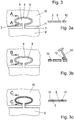
- FIG. 3 A connection process of two elements to be connected together will be explained in greater detail by means of the illustration of FIG Fig. 3 explained in more detail below, wherein, for example, for training, as in Fig. 1d using coupling elements 8 and 9 according to FIG Fig. 2a is shown in Fig. 3 each only a portion of the elements to be joined together is shown. Furthermore is in Fig. 3a, 3b and 3c each on the left side of the illustration, a schematic plan view of such a portion of a combination of cooperating coupling elements 8 and recesses 9 indicated while for the individual process steps in addition to the right side of the illustrations, a section along the lines AA, BB and CC is indicated ,
- Fig. 3a illustrated method step can be seen that to be interconnected elements, which according to the illustration according to Fig. 1d are again denoted by 6 and 10, in the region of their mutually complementary coupling elements and recesses 8 and 9 relative to each other so positioned be maintained that substantially over the entire circumference of the coupling elements 8 and 9 and in the region of mutually facing peripheral regions 7 and 11 in each case a distance 3, in which subsequently an adhesive is introduced.
- the distance 3 is chosen such that it has a maximum width of 500 microns, conveniently 200 microns, so that with large production tolerances, the elements to be joined together, which optionally have additional coupling elements 8 and 9, can be made. Compliance with such a distance of, for example, a maximum of 200 microns allows beyond, as particularly with reference to Fig. 4 will be shown in more detail, also an arrangement of a plurality of elements, which optionally form a plurality of printed circuit boards, on a common carrier element, which can be used for further processing, such as assembly, with tolerances of relative alignment between such a plurality of elements to be arranged of ⁇ 50 microns, in particular ⁇ 30 microns can be achieved or maintained.
- Fig. 3a After arranging the elements to be connected together in a close spatial relationship with each other, as in Fig. 3a is shown in the process step according to Fig. 3b Application of an adhesive 12, for example with a doctor blade 13 using a template 14, so that after the application of the adhesive 12 and a removal of the template 14, as in the method step Fig. 3c is shown, the adhesive 12 has been introduced into the gap 13 for connecting the elements 6 and 10 to be joined together.
- the adhesive 12 which has a high viscosity, favorably introduced only over a portion of the vertical extent of the gap 3, so that in particular when supporting the elements to be joined together 6 and 10, as described below with reference to Fig. 5 will be discussed in detail, a passage of the adhesive 12 to the bottom of the elements 6 and 10 thus adhering the elements a support element can be avoided. Furthermore, from the illustration according to Fig. 3c it can be seen that, in particular, depending on the thickness of the stencil 14 used, the adhesive 12 protrudes only slightly beyond the surface of the elements 6 and 10, so that in particular subsequent processing steps are not hindered or impaired.
- thermosetting or curing adhesive 12 After applying the glue, as in Fig. 3c is indicated, for example, followed by curing using heat or UV light.
- thermosetting or curing adhesive 12 for example, the temperatures between 80 ° C and 200 ° C are selected to avoid in particular an impairment of the already completed printed circuit board elements.
- the adhesive 12 for example, by a screen printing or by an application in the region of the mutually facing peripheral regions 7 and 11 of the elements to be joined together 6 and 10 are applied.
- Such a method makes it possible, for example, to provide a load-bearing capacity of, for example, 2 kg, in particular by increasing or improving the strength of a connection between adjacent elements 6 and 10 by supporting the coupling elements 8 and 9; Processing of such printed circuit boards is sufficient.
- it is ensured that, for example, in subsequent processing or processing steps, such as reflow or soldering, for example, for fixing Of components no changes to the established mechanical connection between the elements 6 and 10 to be joined together occur.
- Fig. 4 is schematically indicated that in a positioning of a plurality of elements 15 in a common element 16 in particular starting from an example of a bore or aperture formed alignment or registration element 17 respectively while maintaining the distance 3 of, for example, a maximum of 200 microns, an orientation of such adjacent elements 15 while maintaining a tolerance of ⁇ 50 microns, in particular ⁇ 30 microns with reference to the individual elements 15 additionally provided alignment elements 18 and 19 can be achieved. Compliance with such low tolerances of a relative orientation is favorable or necessary, in particular, for subsequent processing or processing operations, such as assembly processes, for example, in order to also specify components of such elements 15 that are not shown in detail in a particularly automated manner.
- a carrier element 20 schematically designated 20, which is formed with a plurality of openings or openings 21 for the formation or application of a negative pressure or vacuum by applying a vacuum source, not shown in detail, a plurality of each to be interconnected elements is arranged, which according to the embodiment of Fig. 1d again denoted by 6 and 10.
- a protective layer such as a removable paper layer 22 is arranged, which in turn easily removed after connecting the elements to be joined together 6 and 10 even with a passage of the adhesive over the entire height extent of the peripheral regions to be joined together can be, whereby adhesion to the support member 20 and in particular a contamination of the same with adhesive is prevented.
- a support member designated 30, projecting from the support member 30 elevations or pins 31, which for an at least provisional assurance of interconnecting elements in a again with 6 designated element by schematically indicated openings or openings 32 occur.
- element 6 which is provisionally secured by an interaction of the pins or elevations 31 and the openings 32 on the support member 30, in turn, again 10 designated elements, in particular frame or support elements are connected, which also schematically with 31 indicated pins are secured in their relative positioning to the element 6 to be connected thereto on the carrier element 30, which for the sake of clarity in Fig. 6b not shown.
- an alignment or registration element again denoted by 17, is indicated.
- a provisional securing to the carrier element 20 or 30 may also be provided, for example by clamping the individual elements on the carrier element until application and in particular curing of the adhesive, which in the distance or gap 3 between elements 6 to be joined together or 10 is to be introduced.
- the surface of the support element 20 or 30 facing the elements 6 and 10 to be joined together may be made of a non-slip material such as silicone, rubber or the like be formed or coated with such a material.
- a negative pressure as shown in FIG Fig. 5 is indicated, or provision of additional positioning pins 31 and corresponding recesses or openings 32, as shown in Fig. 6 is implied, one at least provisional securing and positioning of the elements to be joined together 6 and 10 are provided.
- FIG. 7 is indicated schematically that in turn with 6 and 10 denoted, interconnected elements are provisionally secured by an adhesive strip or adhesive label 23 to each other, said adhesive strip 23 after joining the elements 6 and 10 can be removed again.
- Fig. 8 is such a replacement or repair process indicated schematically.
- Fig. 8a which according to Fig. 8b be connected with each other, as for example in Fig. 3 is shown in detail, takes place in the process step according to Fig. 8c a separation of the interconnected circuit board elements I and II along the connection point 25, for example with a cutter or a laser.
- the defective element II can be detached from the element I, as indicated by an arrow 26 in FIG Fig. 8d is indicated, which according to the arrow 27 in Fig. 8e a new element III is used and connected to the element I by means of a bond again denoted by 12.
Landscapes
- Engineering & Computer Science (AREA)
- Microelectronics & Electronic Packaging (AREA)
- Manufacturing & Machinery (AREA)
- Combinations Of Printed Boards (AREA)
- Electric Connection Of Electric Components To Printed Circuits (AREA)
- Structure Of Printed Boards (AREA)
Claims (22)
- Procédé de raccordement d'une pluralité d'éléments d'une carte de circuit imprimé, comprenant les étapes suivantes :- la mise à disposition des éléments (1, 2, 4, 5, 6, 10, 15, 16, I, II, III) d'une carte de circuit imprimé avec des contours adaptés les uns aux autres,- l'agencement des éléments (1, 2, 4, 5, 6, 10, 15, 16, I, II, III) à raccorder les uns aux autres dans un rapport de proximité spatial sur au moins une zone périphérique (7, 11, 28, 29) avec un contour complémentaire l'un à l'autre en respectant une distance (3) entre les zones périphériques (7, 11, 28, 29) tournées les unes vers les autres, et- le raccordement mécanique par collage des zones périphériques (7, 11, 28, 29) tournées les unes vers les autres sur au moins une zone partielle de celles-ci pour le raccordement des éléments (1, 2, 4, 5, 6, 10, 15, 16, I, II, III) à raccorder les uns aux autres de la carte de circuit imprimé, dans lequel les éléments (6, 10) à raccorder l'un à l'autre d'une carte de circuit imprimé sont agencés ou en appui pour la réalisation du processus de raccordement sur un élément porteur (20, 30), les éléments (6, 10) de carte de circuit imprimé à raccorder l'un à l'autre sont maintenus bloqués pendant le processus de raccordement sur l'élément porteur (20, 30) par la création d'un vide, par un serrage, par une entrée d'élévations ou de tiges (31) dépassant de l'élément porteur (30) dans des évidements complémentaires (32) des éléments (6, 10) et/ou la surface dirigée vers les éléments à appuyer (6, 10) de l'élément porteur (20, 30) est formée en un matériau empêchant un glissement, par exemple un silicone, caoutchouc ou similaire ou est revêtue avec celui-ci,caractérisé en ce que la distance (3) entre les zones périphériques (7, 11, 28, 29) à raccorder les unes aux autres et tournées les unes vers les autres est choisie avec 500 µm maximum, en particulier 200 µm maximum.
- Procédé selon la revendication 1, caractérisé en ce que des éléments (15, 16) à raccorder l'un à l'autre sont agencés en référence à au moins un élément d'orientation ou d'enregistrement (17) agencé sur un des éléments à raccorder l'un à l'autre et sont raccordés l'un à l'autre.
- Procédé selon la revendication 1 ou 2, caractérisé en ce qu'une colle (12) durcissant par voie thermique ou chimique ou au moyen de la lumière UV ou lumière IR est utilisée pour le collage.
- Procédé selon la revendication 3, caractérisé en ce qu'un durcissement thermique de la colle (12) est entrepris à une température entre 80 °C et 300 °C.
- Procédé selon la revendication 4, caractérisé en ce qu'une colle (12) à haute viscosité est utilisée.
- Procédé selon l'une quelconque des revendications 1 à 5, caractérisé en ce que la colle (12) est appliquée au moyen d'un dispositif de sortie, d'une impression au pochoir, impression par sérigraphie ou similaire.
- Procédé selon l'une quelconque des revendications 3 à 6, caractérisé en ce que la colle (12) est introduite ou agencée juste sur une zone partielle de l'étendue verticale d'arêtes latérales des zones périphériques (7, 11, 28, 29) à raccorder les unes aux autres.
- Procédé selon l'une quelconque des revendications 1 à 7, caractérisé en ce qu'un raccordement provisoire de zones périphériques (7, 11, 28, 29) à raccorder les unes aux autres est réalisé en utilisant une bande ou étiquette adhésive (23) retirable.
- Procédé selon l'une quelconque des revendications 1 à 8, caractérisé en ce qu'un élément de protection retirable (22) par exemple une couche de papier retirable est agencée sous les zones périphériques à raccorder les unes aux autres des éléments (6, 10) à raccorder l'un à l'autre.
- Procédé selon l'une quelconque des revendications 1 à 9, caractérisé en ce que des éléments (I, II, III) raccordés les unes aux autres d'une carte de circuit imprimé sont séparés les uns des autres par exemple à des fins de réparation, en particulier en utilisant une fraise ou un laser, le long des zones périphériques raccordées les unes aux autres.
- Procédé selon l'une quelconque des revendications 1 à 10, caractérisé en ce que des éléments (6, 10) à raccorder l'un à l'autre sont réalisés sur des zones périphériques (7, 11) à raccorder l'une à l'autre respectivement d'une manière connue en soi avec au moins un élément de couplage (8, 9) complémentaire l'un à l'autre.
- Procédé selon la revendication 11, caractérisé en ce que l'au moins un élément de couplage (8) d'un élément (6) à raccorder l'un à l'autre est formé par un élément de couplage profilé, dépassant de la zone périphérique de l'élément qui est reçu dans un évidement (9) complémentaire de l'élément (10) à raccorder à celui-ci en respectant la distance (3).
- Procédé selon la revendication 11 ou 12, caractérisé en ce qu'un élément (6) sensiblement rectangulaire d'une carte de circuit imprimé est pourvu sur des zones périphériques opposées respectivement les unes aux autres d'au moins un élément de couplage (8) respectif qui est raccordé à un élément de couplage (9) respectif d'un élément (10) de cadre ou de support coagissant avec celui-ci.
- Procédé selon la revendication 11, 12 ou 13, caractérisé en ce qu'une pluralité d'éléments (1, 2, 4, 5, 6, 10, 15, 16, I, II, III) d'une carte de circuit imprimé est raccordée les uns aux autres à distance les uns des autres.
- Carte de circuit imprimé, se composant d'une pluralité d'éléments raccordés les uns aux autres, dans laquelle au moins deux éléments (1 2, 4, 5, 6, 10, 15, 16, I, II, III) à raccorder les uns aux autres de la carte de circuit imprimé sont reliés mécaniquement sur au moins une zone périphérique (7, 11, 28, 29) de ceux-ci en respectant une distance (3) et en appuyant sur un élément de support entre eux par collage, caractérisée en ce que la distance (3) est choisie entre les zones périphériques (7, 11, 28, 29) à raccorder les unes aux autres et tournées les unes vers les autres avec 500 µm maximum, en particulier 200 µm maximum.
- Carte de circuit imprimé selon la revendication 15, caractérisée en ce que des éléments (15, 16) à raccorder l'un à l'autre sont agencés en référence à au moins un élément d'orientation ou d'enregistrement (17) agencé sur un des éléments à raccorder l'un à l'autre et sont raccordés l'un à l'autre.
- Carte de circuit imprimé selon la revendication 15 ou 16, caractérisée en ce qu'une colle (12) durcissant par voie thermique ou chimique ou au moyen d'une lumière UV ou lumière IR est utilisée pour le collage.
- Carte de circuit imprimé selon la revendication 17, caractérisée en ce que la colle (12) est introduite ou agencée juste sur une zone partielle de l'étendue verticale d'arêtes latérales des zones périphériques (7, 11, 28, 29) à raccorder les unes aux autres.
- Carte de circuit imprimé selon l'une quelconque des revendications 15 à 18, caractérisée en ce que des éléments (I, II, III) à raccorder les uns aux autres d'une carte de circuit imprimé sont séparables les uns des autres par exemple à des fins de réparation en particulier en utilisant une fraise ou un laser le long des zones périphériques raccordées les unes aux autres.
- Carte de circuit imprimé selon l'une quelconque des revendications 15 à 19, caractérisée en ce que des éléments (6, 10) à raccorder l'un à l'autre sont réalisés sur des zones périphériques (7, 11) à raccorder l'une à l'autre d'une manière connue en soi respectivement avec au moins un élément de couplage (8, 9) complémentaire l'un à l'autre.
- Carte de circuit imprimé selon la revendication 20, caractérisée en ce que l'au moins un élément de couplage (8) d'un élément (6) à raccorder l'un à l'autre est formé d'un élément de couplage profilé dépassant de la zone périphérique (7) de l'élément, qui est reçu dans un évidement (9) complémentaire de l'élément (10) à raccorder à celui-ci en respectant la distance.
- Utilisation du procédé selon l'une quelconque des revendications 1 à 14 pour la fabrication d'une carte de circuit imprimé en plusieurs parties.
Applications Claiming Priority (2)
| Application Number | Priority Date | Filing Date | Title |
|---|---|---|---|
| AT0055209U AT12320U1 (de) | 2009-09-03 | 2009-09-03 | Verfahren zum verbinden einer mehrzahl von elementen einer leiterplatte, leiterplatte sowie verwendung eines derartigen verfahrens |
| PCT/AT2010/000316 WO2011026165A1 (fr) | 2009-09-03 | 2010-09-01 | Procédé permettant de connecter plusieurs éléments d'une carte de circuit imprimé, carte de circuit imprimé et utilisation d'un tel procédé |
Publications (2)
| Publication Number | Publication Date |
|---|---|
| EP2474209A1 EP2474209A1 (fr) | 2012-07-11 |
| EP2474209B1 true EP2474209B1 (fr) | 2018-10-31 |
Family
ID=43064794
Family Applications (1)
| Application Number | Title | Priority Date | Filing Date |
|---|---|---|---|
| EP10755076.6A Active EP2474209B1 (fr) | 2009-09-03 | 2010-09-01 | Procédé permettant de connecter plusieurs éléments d'une carte de circuit imprimé, carte de circuit imprimé et utilisation d'un tel procédé |
Country Status (7)
| Country | Link |
|---|---|
| US (2) | US8863375B2 (fr) |
| EP (1) | EP2474209B1 (fr) |
| JP (1) | JP2013504182A (fr) |
| CN (1) | CN102656954B (fr) |
| AT (1) | AT12320U1 (fr) |
| TW (1) | TW201125451A (fr) |
| WO (1) | WO2011026165A1 (fr) |
Families Citing this family (10)
| Publication number | Priority date | Publication date | Assignee | Title |
|---|---|---|---|---|
| JP2013197455A (ja) * | 2012-03-22 | 2013-09-30 | Bosch Corp | プリント回路基板の製造方法及びプリント回路基板の修理方法 |
| TWI461127B (zh) * | 2012-12-25 | 2014-11-11 | Univ Nat Taipei Technology | 電子裝置及其製法 |
| US9084362B2 (en) * | 2013-01-08 | 2015-07-14 | Nvidia Corporation | Reducing impedance of a printed circuit board through a square wave pattern of plated-through holes |
| CN203151864U (zh) | 2013-03-05 | 2013-08-21 | 奥特斯(中国)有限公司 | 印制电路板 |
| AT514074B1 (de) * | 2013-04-02 | 2014-10-15 | Austria Tech & System Tech | Verfahren zum Herstellen eines Leiterplattenelements |
| JP6051410B2 (ja) * | 2013-09-24 | 2016-12-27 | パナソニックIpマネジメント株式会社 | 部品実装装置 |
| DE102014008148B4 (de) * | 2014-05-23 | 2020-06-04 | Continental Automotive Gmbh | Verfahren zur Herstellung einer Leiterplatte und Leiterplatte |
| WO2016156598A1 (fr) | 2015-04-01 | 2016-10-06 | Philip Morris Products S.A. | Substance de tabac homogénéisée et procédé de production de substance de tabac homogénéisée |
| EP3548653A1 (fr) | 2016-11-29 | 2019-10-09 | Advanced Materials Design & Manufacturing Limited | Procédé de fabrication de textiles hybrides (en fibres-nanofibres) par l'intermédiaire de liaisons efficaces de fibres à nanofibres comprenant de nouveaux mécanismes de transfert de charge efficaces |
| US11189610B2 (en) * | 2018-06-27 | 2021-11-30 | Advanced Semiconductor Engineering, Inc. | Substrate structure and manufacturing process |
Citations (1)
| Publication number | Priority date | Publication date | Assignee | Title |
|---|---|---|---|---|
| US20020152609A1 (en) * | 1999-02-23 | 2002-10-24 | Samsung Electro-Mechanics Co., Ltd. | Method and device for coupling PCB sheet |
Family Cites Families (22)
| Publication number | Priority date | Publication date | Assignee | Title |
|---|---|---|---|---|
| US4255003A (en) * | 1975-11-13 | 1981-03-10 | Tektronix, Inc. | Electrical connector |
| US4293175A (en) * | 1978-06-08 | 1981-10-06 | Cutchaw John M | Connector for integrated circuit packages |
| JPS61265219A (ja) * | 1985-05-20 | 1986-11-25 | Hitachi Electronics Eng Co Ltd | 基板位置決め方法 |
| US4689103A (en) | 1985-11-18 | 1987-08-25 | E. I. Du Pont De Nemours And Company | Method of manufacturing injection molded printed circuit boards in a common planar array |
| EP0360971A3 (fr) * | 1988-08-31 | 1991-07-17 | Mitsui Mining & Smelting Co., Ltd. | Substrat de montage et sa méthode de production et circuit imprimé ayant une fonction de connecteur et sa méthode de connexion |
| US5044615A (en) | 1991-02-08 | 1991-09-03 | International Business Machines Corporation | Dual purpose work board holder |
| DE19600928A1 (de) | 1996-01-12 | 1997-07-24 | Ibm | Vorrichtung zur Handhabung von Leiterplatten und deren Herstellung |
| TW492114B (en) * | 2000-06-19 | 2002-06-21 | Advantest Corp | Method and apparatus for edge connection between elements of an integrated circuit |
| US6727591B2 (en) * | 2001-03-26 | 2004-04-27 | Ibiden Co., Ltd. | Multi-piece substrate and method of manufacturing the substrate |
| DE10131945A1 (de) | 2001-07-02 | 2003-01-30 | Siemens Dematic Ag | Verfahren zum gemeinsamen Bearbeiten von Leiterplatten |
| US6817527B2 (en) * | 2002-06-28 | 2004-11-16 | Nokia Corporation | Carriers for printed circuit board marking |
| WO2004023859A1 (fr) * | 2002-09-03 | 2004-03-18 | Pcb Plus, Inc. | Appareil et procede de remplacement de carte a circuit imprime defectueuse sur un panneau a cartes a circuits imprimes |
| JP3751938B2 (ja) * | 2002-12-09 | 2006-03-08 | 日東電工株式会社 | Tab用テープキャリアおよびその製造方法 |
| US7413481B2 (en) * | 2003-09-26 | 2008-08-19 | Redmond Iii Frank E | Systems for and methods of circuit construction |
| TWM257001U (en) * | 2003-11-27 | 2005-02-11 | Optimum Care Int Tech Inc | Improved memory module |
| JP2005322878A (ja) * | 2004-04-09 | 2005-11-17 | Dainippon Printing Co Ltd | 印刷配線基板の組付パネル、印刷配線基板の実装用単位シート、リジッド−フレキシブル基板及びこれらの製造方法 |
| US20080144299A1 (en) * | 2004-07-15 | 2008-06-19 | Redmond Frank E | Systems for and methods of circuit construction |
| FI20070910A0 (fi) | 2007-11-27 | 2007-11-27 | Kimmo Olavi Paananen | Menetelmä piirilevyjen panelisointiin |
| US8698004B2 (en) * | 2008-10-27 | 2014-04-15 | Ibiden Co., Ltd. | Multi-piece board and fabrication method thereof |
| US8119454B2 (en) * | 2008-12-08 | 2012-02-21 | Stmicroelectronics Asia Pacific Pte Ltd. | Manufacturing fan-out wafer level packaging |
| CN101971719B (zh) * | 2009-06-04 | 2013-01-16 | 揖斐电株式会社 | 多连片基板的制造方法以及多连片基板 |
| US8547702B2 (en) * | 2009-10-26 | 2013-10-01 | Ibiden Co., Ltd. | Multi-piece board and method for manufacturing the same |
-
2009
- 2009-09-03 AT AT0055209U patent/AT12320U1/de not_active IP Right Cessation
-
2010
- 2010-09-01 US US13/393,697 patent/US8863375B2/en not_active Expired - Fee Related
- 2010-09-01 EP EP10755076.6A patent/EP2474209B1/fr active Active
- 2010-09-01 WO PCT/AT2010/000316 patent/WO2011026165A1/fr not_active Ceased
- 2010-09-01 JP JP2012527154A patent/JP2013504182A/ja active Pending
- 2010-09-01 CN CN201080039334.XA patent/CN102656954B/zh active Active
- 2010-09-03 TW TW099129817A patent/TW201125451A/zh unknown
-
2014
- 2014-09-19 US US14/490,840 patent/US20150014021A1/en not_active Abandoned
Patent Citations (1)
| Publication number | Priority date | Publication date | Assignee | Title |
|---|---|---|---|---|
| US20020152609A1 (en) * | 1999-02-23 | 2002-10-24 | Samsung Electro-Mechanics Co., Ltd. | Method and device for coupling PCB sheet |
Also Published As
| Publication number | Publication date |
|---|---|
| CN102656954B (zh) | 2016-09-07 |
| US8863375B2 (en) | 2014-10-21 |
| WO2011026165A1 (fr) | 2011-03-10 |
| EP2474209A1 (fr) | 2012-07-11 |
| CN102656954A (zh) | 2012-09-05 |
| JP2013504182A (ja) | 2013-02-04 |
| TW201125451A (en) | 2011-07-16 |
| US20120160555A1 (en) | 2012-06-28 |
| AT12320U1 (de) | 2012-03-15 |
| US20150014021A1 (en) | 2015-01-15 |
Similar Documents
| Publication | Publication Date | Title |
|---|---|---|
| EP2474209B1 (fr) | Procédé permettant de connecter plusieurs éléments d'une carte de circuit imprimé, carte de circuit imprimé et utilisation d'un tel procédé | |
| EP2027600B1 (fr) | Procédé pour noyer au moins un composant dans un élément de carte de circuits imprimés | |
| EP2407014B1 (fr) | Procédé et système de connexion d'une pluralité de cartes de circuit imprimé à au moins un élément support ou cadre | |
| EP3940758A2 (fr) | Procédé de connexion par frittage d'un agencement de substrat avec un composant électronique utilisant un moyen de pré-fixation sur une couche de matériau de frittage de contact, agencement de substrat correspondant et procédé de sa fabrication | |
| EP1550358B1 (fr) | Carte de circuit imprime presentant au moins une partie rigide et une partie souple et procede de production de cartes de circuits imprimes rigides et souples | |
| WO2017125385A1 (fr) | Procédé de pose d'étiquettes de repérage sur une pluralité d'appareils électriques pouvant être rangés sur un rail porteur | |
| DE102016100722A1 (de) | Verfahren zum Anbringen von Markierungsschildern an einer Mehrzahl von an einer Tragschiene anordbaren elektrischen Geräten | |
| DE10145749A1 (de) | Verfahren zur Herstellung einer strukturierten Metallschicht auf einem Trägerkörper und Trägerkörper mit einer strukturierten Metallschicht | |
| EP3026702B1 (fr) | Procede de fabrication d'un element semi-conducteur dote d'un adaptateur de substrat et element semi-conducteur dote d'un adaptateur de substrat | |
| EP2982226B1 (fr) | Procédé de fabrication d'un élément de circuit imprimé | |
| DE102010015408B4 (de) | Schmelzklebstoffeinheit einer Klebeanordnung | |
| WO2016005146A1 (fr) | Procédé de production d'un adaptateur de substrat, adaptateur de substrat et procédé d'interconnexion d'un élément semi-conducteur | |
| EP2789214B1 (fr) | Procédé de production d'une carte de circuit par élimination d'une zone partielle de ladite carte, et utilisation d'un tel procédé | |
| AT12738U1 (de) | Verfahren und system zum bereitstellen eines insbesondere eine mehrzahl von leiterplattenelementen enthaltenden plattenförmigen gegenstands | |
| EP0126856A2 (fr) | Procédé de fabrication d'une plaquette de circuit comportant des domaines rigides et flexibles | |
| DE20221189U1 (de) | Leiterplatte mit mindestens einem starren Bereich und mindestens einem flexiblen Bereich | |
| DE3302857A1 (de) | Verfahren zum herstellen von vorlaminaten fuer starrflexible leiterplatten | |
| EP3120676A1 (fr) | Module de commande électronique et procédé servant à fabriquer ledit module | |
| DE19819054B4 (de) | Verfahren und Vorrichtung zur Montage und Justierung von Bauteilen auf einer Befestigungsunterlage | |
| EP2768290A1 (fr) | Composant électronique | |
| EP2692215B1 (fr) | Procédé de fabrication, en particulier d'usinage ou d'équipement, d'un élément de carte de circuits imprimés, ainsi que support destiné à être utilisé dans un tel procédé | |
| DE102005027276B3 (de) | Verfahren zur Herstellung einer Stapelanordnung | |
| DE19830628C1 (de) | Verfahren zum Verpressen von Mehrlagenleiterplatten (Multilayer) | |
| WO2011113073A1 (fr) | Procédé et combinaison pour traiter ou manipuler une pluralité de cartes de circuits imprimés et leur application | |
| DE10258090B4 (de) | Verfahren zur Herstellung von starr-flexiblen Leiterplatten und Leiterplatten mit mindestens einem starren Bereich und mindestens einem flexiblen Bereich |
Legal Events
| Date | Code | Title | Description |
|---|---|---|---|
| PUAI | Public reference made under article 153(3) epc to a published international application that has entered the european phase |
Free format text: ORIGINAL CODE: 0009012 |
|
| 17P | Request for examination filed |
Effective date: 20120327 |
|
| AK | Designated contracting states |
Kind code of ref document: A1 Designated state(s): AL AT BE BG CH CY CZ DE DK EE ES FI FR GB GR HR HU IE IS IT LI LT LU LV MC MK MT NL NO PL PT RO SE SI SK SM TR |
|
| DAX | Request for extension of the european patent (deleted) | ||
| TPAC | Observations filed by third parties |
Free format text: ORIGINAL CODE: EPIDOSNTIPA |
|
| 17Q | First examination report despatched |
Effective date: 20141201 |
|
| GRAP | Despatch of communication of intention to grant a patent |
Free format text: ORIGINAL CODE: EPIDOSNIGR1 |
|
| STAA | Information on the status of an ep patent application or granted ep patent |
Free format text: STATUS: GRANT OF PATENT IS INTENDED |
|
| INTG | Intention to grant announced |
Effective date: 20180409 |
|
| GRAS | Grant fee paid |
Free format text: ORIGINAL CODE: EPIDOSNIGR3 |
|
| GRAJ | Information related to disapproval of communication of intention to grant by the applicant or resumption of examination proceedings by the epo deleted |
Free format text: ORIGINAL CODE: EPIDOSDIGR1 |
|
| GRAL | Information related to payment of fee for publishing/printing deleted |
Free format text: ORIGINAL CODE: EPIDOSDIGR3 |
|
| STAA | Information on the status of an ep patent application or granted ep patent |
Free format text: STATUS: EXAMINATION IS IN PROGRESS |
|
| GRAR | Information related to intention to grant a patent recorded |
Free format text: ORIGINAL CODE: EPIDOSNIGR71 |
|
| STAA | Information on the status of an ep patent application or granted ep patent |
Free format text: STATUS: GRANT OF PATENT IS INTENDED |
|
| INTC | Intention to grant announced (deleted) | ||
| GRAA | (expected) grant |
Free format text: ORIGINAL CODE: 0009210 |
|
| STAA | Information on the status of an ep patent application or granted ep patent |
Free format text: STATUS: THE PATENT HAS BEEN GRANTED |
|
| INTG | Intention to grant announced |
Effective date: 20180906 |
|
| AK | Designated contracting states |
Kind code of ref document: B1 Designated state(s): AL AT BE BG CH CY CZ DE DK EE ES FI FR GB GR HR HU IE IS IT LI LT LU LV MC MK MT NL NO PL PT RO SE SI SK SM TR |
|
| REG | Reference to a national code |
Ref country code: CH Ref legal event code: EP Ref country code: GB Ref legal event code: FG4D Free format text: NOT ENGLISH |
|
| REG | Reference to a national code |
Ref country code: AT Ref legal event code: REF Ref document number: 1060964 Country of ref document: AT Kind code of ref document: T Effective date: 20181115 |
|
| REG | Reference to a national code |
Ref country code: DE Ref legal event code: R096 Ref document number: 502010015522 Country of ref document: DE |
|
| REG | Reference to a national code |
Ref country code: IE Ref legal event code: FG4D Free format text: LANGUAGE OF EP DOCUMENT: GERMAN |
|
| REG | Reference to a national code |
Ref country code: NL Ref legal event code: MP Effective date: 20181031 |
|
| REG | Reference to a national code |
Ref country code: LT Ref legal event code: MG4D |
|
| PG25 | Lapsed in a contracting state [announced via postgrant information from national office to epo] |
Ref country code: HR Free format text: LAPSE BECAUSE OF FAILURE TO SUBMIT A TRANSLATION OF THE DESCRIPTION OR TO PAY THE FEE WITHIN THE PRESCRIBED TIME-LIMIT Effective date: 20181031 Ref country code: LT Free format text: LAPSE BECAUSE OF FAILURE TO SUBMIT A TRANSLATION OF THE DESCRIPTION OR TO PAY THE FEE WITHIN THE PRESCRIBED TIME-LIMIT Effective date: 20181031 Ref country code: IS Free format text: LAPSE BECAUSE OF FAILURE TO SUBMIT A TRANSLATION OF THE DESCRIPTION OR TO PAY THE FEE WITHIN THE PRESCRIBED TIME-LIMIT Effective date: 20190228 Ref country code: PL Free format text: LAPSE BECAUSE OF FAILURE TO SUBMIT A TRANSLATION OF THE DESCRIPTION OR TO PAY THE FEE WITHIN THE PRESCRIBED TIME-LIMIT Effective date: 20181031 Ref country code: BG Free format text: LAPSE BECAUSE OF FAILURE TO SUBMIT A TRANSLATION OF THE DESCRIPTION OR TO PAY THE FEE WITHIN THE PRESCRIBED TIME-LIMIT Effective date: 20190131 Ref country code: FI Free format text: LAPSE BECAUSE OF FAILURE TO SUBMIT A TRANSLATION OF THE DESCRIPTION OR TO PAY THE FEE WITHIN THE PRESCRIBED TIME-LIMIT Effective date: 20181031 Ref country code: LV Free format text: LAPSE BECAUSE OF FAILURE TO SUBMIT A TRANSLATION OF THE DESCRIPTION OR TO PAY THE FEE WITHIN THE PRESCRIBED TIME-LIMIT Effective date: 20181031 Ref country code: ES Free format text: LAPSE BECAUSE OF FAILURE TO SUBMIT A TRANSLATION OF THE DESCRIPTION OR TO PAY THE FEE WITHIN THE PRESCRIBED TIME-LIMIT Effective date: 20181031 Ref country code: NO Free format text: LAPSE BECAUSE OF FAILURE TO SUBMIT A TRANSLATION OF THE DESCRIPTION OR TO PAY THE FEE WITHIN THE PRESCRIBED TIME-LIMIT Effective date: 20190131 |
|
| PG25 | Lapsed in a contracting state [announced via postgrant information from national office to epo] |
Ref country code: PT Free format text: LAPSE BECAUSE OF FAILURE TO SUBMIT A TRANSLATION OF THE DESCRIPTION OR TO PAY THE FEE WITHIN THE PRESCRIBED TIME-LIMIT Effective date: 20190301 Ref country code: NL Free format text: LAPSE BECAUSE OF FAILURE TO SUBMIT A TRANSLATION OF THE DESCRIPTION OR TO PAY THE FEE WITHIN THE PRESCRIBED TIME-LIMIT Effective date: 20181031 Ref country code: AL Free format text: LAPSE BECAUSE OF FAILURE TO SUBMIT A TRANSLATION OF THE DESCRIPTION OR TO PAY THE FEE WITHIN THE PRESCRIBED TIME-LIMIT Effective date: 20181031 Ref country code: GR Free format text: LAPSE BECAUSE OF FAILURE TO SUBMIT A TRANSLATION OF THE DESCRIPTION OR TO PAY THE FEE WITHIN THE PRESCRIBED TIME-LIMIT Effective date: 20190201 Ref country code: SE Free format text: LAPSE BECAUSE OF FAILURE TO SUBMIT A TRANSLATION OF THE DESCRIPTION OR TO PAY THE FEE WITHIN THE PRESCRIBED TIME-LIMIT Effective date: 20181031 |
|
| PG25 | Lapsed in a contracting state [announced via postgrant information from national office to epo] |
Ref country code: DK Free format text: LAPSE BECAUSE OF FAILURE TO SUBMIT A TRANSLATION OF THE DESCRIPTION OR TO PAY THE FEE WITHIN THE PRESCRIBED TIME-LIMIT Effective date: 20181031 Ref country code: CZ Free format text: LAPSE BECAUSE OF FAILURE TO SUBMIT A TRANSLATION OF THE DESCRIPTION OR TO PAY THE FEE WITHIN THE PRESCRIBED TIME-LIMIT Effective date: 20181031 Ref country code: IT Free format text: LAPSE BECAUSE OF FAILURE TO SUBMIT A TRANSLATION OF THE DESCRIPTION OR TO PAY THE FEE WITHIN THE PRESCRIBED TIME-LIMIT Effective date: 20181031 |
|
| REG | Reference to a national code |
Ref country code: DE Ref legal event code: R097 Ref document number: 502010015522 Country of ref document: DE |
|
| PG25 | Lapsed in a contracting state [announced via postgrant information from national office to epo] |
Ref country code: SK Free format text: LAPSE BECAUSE OF FAILURE TO SUBMIT A TRANSLATION OF THE DESCRIPTION OR TO PAY THE FEE WITHIN THE PRESCRIBED TIME-LIMIT Effective date: 20181031 Ref country code: EE Free format text: LAPSE BECAUSE OF FAILURE TO SUBMIT A TRANSLATION OF THE DESCRIPTION OR TO PAY THE FEE WITHIN THE PRESCRIBED TIME-LIMIT Effective date: 20181031 Ref country code: SM Free format text: LAPSE BECAUSE OF FAILURE TO SUBMIT A TRANSLATION OF THE DESCRIPTION OR TO PAY THE FEE WITHIN THE PRESCRIBED TIME-LIMIT Effective date: 20181031 Ref country code: RO Free format text: LAPSE BECAUSE OF FAILURE TO SUBMIT A TRANSLATION OF THE DESCRIPTION OR TO PAY THE FEE WITHIN THE PRESCRIBED TIME-LIMIT Effective date: 20181031 |
|
| PLBE | No opposition filed within time limit |
Free format text: ORIGINAL CODE: 0009261 |
|
| STAA | Information on the status of an ep patent application or granted ep patent |
Free format text: STATUS: NO OPPOSITION FILED WITHIN TIME LIMIT |
|
| 26N | No opposition filed |
Effective date: 20190801 |
|
| PG25 | Lapsed in a contracting state [announced via postgrant information from national office to epo] |
Ref country code: SI Free format text: LAPSE BECAUSE OF FAILURE TO SUBMIT A TRANSLATION OF THE DESCRIPTION OR TO PAY THE FEE WITHIN THE PRESCRIBED TIME-LIMIT Effective date: 20181031 |
|
| PG25 | Lapsed in a contracting state [announced via postgrant information from national office to epo] |
Ref country code: TR Free format text: LAPSE BECAUSE OF FAILURE TO SUBMIT A TRANSLATION OF THE DESCRIPTION OR TO PAY THE FEE WITHIN THE PRESCRIBED TIME-LIMIT Effective date: 20181031 |
|
| PG25 | Lapsed in a contracting state [announced via postgrant information from national office to epo] |
Ref country code: MC Free format text: LAPSE BECAUSE OF FAILURE TO SUBMIT A TRANSLATION OF THE DESCRIPTION OR TO PAY THE FEE WITHIN THE PRESCRIBED TIME-LIMIT Effective date: 20181031 |
|
| REG | Reference to a national code |
Ref country code: CH Ref legal event code: PL |
|
| PG25 | Lapsed in a contracting state [announced via postgrant information from national office to epo] |
Ref country code: LU Free format text: LAPSE BECAUSE OF NON-PAYMENT OF DUE FEES Effective date: 20190901 Ref country code: LI Free format text: LAPSE BECAUSE OF NON-PAYMENT OF DUE FEES Effective date: 20190930 Ref country code: CH Free format text: LAPSE BECAUSE OF NON-PAYMENT OF DUE FEES Effective date: 20190930 Ref country code: IE Free format text: LAPSE BECAUSE OF NON-PAYMENT OF DUE FEES Effective date: 20190901 |
|
| REG | Reference to a national code |
Ref country code: BE Ref legal event code: MM Effective date: 20190930 |
|
| PG25 | Lapsed in a contracting state [announced via postgrant information from national office to epo] |
Ref country code: BE Free format text: LAPSE BECAUSE OF NON-PAYMENT OF DUE FEES Effective date: 20190930 |
|
| GBPC | Gb: european patent ceased through non-payment of renewal fee |
Effective date: 20190901 |
|
| PG25 | Lapsed in a contracting state [announced via postgrant information from national office to epo] |
Ref country code: GB Free format text: LAPSE BECAUSE OF NON-PAYMENT OF DUE FEES Effective date: 20190901 |
|
| REG | Reference to a national code |
Ref country code: AT Ref legal event code: MM01 Ref document number: 1060964 Country of ref document: AT Kind code of ref document: T Effective date: 20190901 |
|
| PG25 | Lapsed in a contracting state [announced via postgrant information from national office to epo] |
Ref country code: AT Free format text: LAPSE BECAUSE OF NON-PAYMENT OF DUE FEES Effective date: 20190901 |
|
| PG25 | Lapsed in a contracting state [announced via postgrant information from national office to epo] |
Ref country code: CY Free format text: LAPSE BECAUSE OF FAILURE TO SUBMIT A TRANSLATION OF THE DESCRIPTION OR TO PAY THE FEE WITHIN THE PRESCRIBED TIME-LIMIT Effective date: 20181031 |
|
| PG25 | Lapsed in a contracting state [announced via postgrant information from national office to epo] |
Ref country code: MT Free format text: LAPSE BECAUSE OF FAILURE TO SUBMIT A TRANSLATION OF THE DESCRIPTION OR TO PAY THE FEE WITHIN THE PRESCRIBED TIME-LIMIT Effective date: 20181031 Ref country code: HU Free format text: LAPSE BECAUSE OF FAILURE TO SUBMIT A TRANSLATION OF THE DESCRIPTION OR TO PAY THE FEE WITHIN THE PRESCRIBED TIME-LIMIT; INVALID AB INITIO Effective date: 20100901 |
|
| PG25 | Lapsed in a contracting state [announced via postgrant information from national office to epo] |
Ref country code: MK Free format text: LAPSE BECAUSE OF FAILURE TO SUBMIT A TRANSLATION OF THE DESCRIPTION OR TO PAY THE FEE WITHIN THE PRESCRIBED TIME-LIMIT Effective date: 20181031 |
|
| P01 | Opt-out of the competence of the unified patent court (upc) registered |
Effective date: 20230526 |
|
| PGFP | Annual fee paid to national office [announced via postgrant information from national office to epo] |
Ref country code: DE Payment date: 20250917 Year of fee payment: 16 |
|
| PGFP | Annual fee paid to national office [announced via postgrant information from national office to epo] |
Ref country code: FR Payment date: 20250926 Year of fee payment: 16 |