EP2477227B1 - Magnettunnelübergang mit einer Polarisierungsschicht - Google Patents
Magnettunnelübergang mit einer Polarisierungsschicht Download PDFInfo
- Publication number
- EP2477227B1 EP2477227B1 EP11290013.9A EP11290013A EP2477227B1 EP 2477227 B1 EP2477227 B1 EP 2477227B1 EP 11290013 A EP11290013 A EP 11290013A EP 2477227 B1 EP2477227 B1 EP 2477227B1
- Authority
- EP
- European Patent Office
- Prior art keywords
- layer
- magnetization
- tunnel junction
- ferromagnetic
- magnetic tunnel
- Prior art date
- Legal status (The legal status is an assumption and is not a legal conclusion. Google has not performed a legal analysis and makes no representation as to the accuracy of the status listed.)
- Active
Links
- 230000005291 magnetic effect Effects 0.000 title claims description 55
- 230000005294 ferromagnetic effect Effects 0.000 claims description 55
- 230000005415 magnetization Effects 0.000 claims description 52
- 238000000137 annealing Methods 0.000 claims description 31
- 230000004888 barrier function Effects 0.000 claims description 17
- 238000000034 method Methods 0.000 claims description 17
- 238000000151 deposition Methods 0.000 claims description 12
- 238000004519 manufacturing process Methods 0.000 claims description 4
- 238000003860 storage Methods 0.000 description 8
- CPLXHLVBOLITMK-UHFFFAOYSA-N magnesium oxide Inorganic materials [Mg]=O CPLXHLVBOLITMK-UHFFFAOYSA-N 0.000 description 7
- 239000000395 magnesium oxide Substances 0.000 description 7
- AXZKOIWUVFPNLO-UHFFFAOYSA-N magnesium;oxygen(2-) Chemical compound [O-2].[Mg+2] AXZKOIWUVFPNLO-UHFFFAOYSA-N 0.000 description 7
- 239000000956 alloy Substances 0.000 description 5
- 229910045601 alloy Inorganic materials 0.000 description 5
- KDLHZDBZIXYQEI-UHFFFAOYSA-N Palladium Chemical compound [Pd] KDLHZDBZIXYQEI-UHFFFAOYSA-N 0.000 description 4
- 230000015654 memory Effects 0.000 description 4
- BASFCYQUMIYNBI-UHFFFAOYSA-N platinum Chemical compound [Pt] BASFCYQUMIYNBI-UHFFFAOYSA-N 0.000 description 4
- PXHVJJICTQNCMI-UHFFFAOYSA-N Nickel Chemical compound [Ni] PXHVJJICTQNCMI-UHFFFAOYSA-N 0.000 description 3
- 230000005290 antiferromagnetic effect Effects 0.000 description 3
- 229910017052 cobalt Inorganic materials 0.000 description 3
- 239000010941 cobalt Substances 0.000 description 3
- GUTLYIVDDKVIGB-UHFFFAOYSA-N cobalt atom Chemical compound [Co] GUTLYIVDDKVIGB-UHFFFAOYSA-N 0.000 description 3
- 229910052763 palladium Inorganic materials 0.000 description 3
- 229910052697 platinum Inorganic materials 0.000 description 3
- PNEYBMLMFCGWSK-UHFFFAOYSA-N aluminium oxide Inorganic materials [O-2].[O-2].[O-2].[Al+3].[Al+3] PNEYBMLMFCGWSK-UHFFFAOYSA-N 0.000 description 2
- 230000003247 decreasing effect Effects 0.000 description 2
- 229910052742 iron Inorganic materials 0.000 description 2
- 229910052759 nickel Inorganic materials 0.000 description 2
- 229910052723 transition metal Inorganic materials 0.000 description 2
- 150000003624 transition metals Chemical class 0.000 description 2
- ZOXJGFHDIHLPTG-UHFFFAOYSA-N Boron Chemical compound [B] ZOXJGFHDIHLPTG-UHFFFAOYSA-N 0.000 description 1
- 230000006399 behavior Effects 0.000 description 1
- 229910052796 boron Inorganic materials 0.000 description 1
- 239000003990 capacitor Substances 0.000 description 1
- 238000004891 communication Methods 0.000 description 1
- 229910052593 corundum Inorganic materials 0.000 description 1
- 230000001419 dependent effect Effects 0.000 description 1
- 238000005516 engineering process Methods 0.000 description 1
- 239000003302 ferromagnetic material Substances 0.000 description 1
- 230000005865 ionizing radiation Effects 0.000 description 1
- 239000000696 magnetic material Substances 0.000 description 1
- 229910052751 metal Inorganic materials 0.000 description 1
- 239000002184 metal Substances 0.000 description 1
- 150000002739 metals Chemical class 0.000 description 1
- 239000000203 mixture Substances 0.000 description 1
- 230000000149 penetrating effect Effects 0.000 description 1
- 230000010287 polarization Effects 0.000 description 1
- 229910052761 rare earth metal Inorganic materials 0.000 description 1
- 150000002910 rare earth metals Chemical class 0.000 description 1
- 238000007725 thermal activation Methods 0.000 description 1
- 230000007704 transition Effects 0.000 description 1
- 230000001960 triggered effect Effects 0.000 description 1
- 229910001845 yogo sapphire Inorganic materials 0.000 description 1
Images
Classifications
-
- H—ELECTRICITY
- H10—SEMICONDUCTOR DEVICES; ELECTRIC SOLID-STATE DEVICES NOT OTHERWISE PROVIDED FOR
- H10N—ELECTRIC SOLID-STATE DEVICES NOT OTHERWISE PROVIDED FOR
- H10N50/00—Galvanomagnetic devices
- H10N50/10—Magnetoresistive devices
-
- B—PERFORMING OPERATIONS; TRANSPORTING
- B82—NANOTECHNOLOGY
- B82Y—SPECIFIC USES OR APPLICATIONS OF NANOSTRUCTURES; MEASUREMENT OR ANALYSIS OF NANOSTRUCTURES; MANUFACTURE OR TREATMENT OF NANOSTRUCTURES
- B82Y10/00—Nanotechnology for information processing, storage or transmission, e.g. quantum computing or single electron logic
-
- B—PERFORMING OPERATIONS; TRANSPORTING
- B82—NANOTECHNOLOGY
- B82Y—SPECIFIC USES OR APPLICATIONS OF NANOSTRUCTURES; MEASUREMENT OR ANALYSIS OF NANOSTRUCTURES; MANUFACTURE OR TREATMENT OF NANOSTRUCTURES
- B82Y25/00—Nanomagnetism, e.g. magnetoimpedance, anisotropic magnetoresistance, giant magnetoresistance or tunneling magnetoresistance
-
- G—PHYSICS
- G11—INFORMATION STORAGE
- G11C—STATIC STORES
- G11C11/00—Digital stores characterised by the use of particular electric or magnetic storage elements; Storage elements therefor
- G11C11/02—Digital stores characterised by the use of particular electric or magnetic storage elements; Storage elements therefor using magnetic elements
- G11C11/16—Digital stores characterised by the use of particular electric or magnetic storage elements; Storage elements therefor using magnetic elements using elements in which the storage effect is based on magnetic spin effect
- G11C11/161—Digital stores characterised by the use of particular electric or magnetic storage elements; Storage elements therefor using magnetic elements using elements in which the storage effect is based on magnetic spin effect details concerning the memory cell structure, e.g. the layers of the ferromagnetic memory cell
-
- G—PHYSICS
- G11—INFORMATION STORAGE
- G11C—STATIC STORES
- G11C11/00—Digital stores characterised by the use of particular electric or magnetic storage elements; Storage elements therefor
- G11C11/02—Digital stores characterised by the use of particular electric or magnetic storage elements; Storage elements therefor using magnetic elements
- G11C11/16—Digital stores characterised by the use of particular electric or magnetic storage elements; Storage elements therefor using magnetic elements using elements in which the storage effect is based on magnetic spin effect
- G11C11/165—Auxiliary circuits
- G11C11/1675—Writing or programming circuits or methods
-
- H—ELECTRICITY
- H01—ELECTRIC ELEMENTS
- H01F—MAGNETS; INDUCTANCES; TRANSFORMERS; SELECTION OF MATERIALS FOR THEIR MAGNETIC PROPERTIES
- H01F10/00—Thin magnetic films, e.g. of one-domain structure
- H01F10/32—Spin-exchange-coupled multilayers, e.g. nanostructured superlattices
- H01F10/324—Exchange coupling of magnetic film pairs via a very thin non-magnetic spacer, e.g. by exchange with conduction electrons of the spacer
- H01F10/3286—Spin-exchange coupled multilayers having at least one layer with perpendicular magnetic anisotropy
-
- H—ELECTRICITY
- H01—ELECTRIC ELEMENTS
- H01F—MAGNETS; INDUCTANCES; TRANSFORMERS; SELECTION OF MATERIALS FOR THEIR MAGNETIC PROPERTIES
- H01F10/00—Thin magnetic films, e.g. of one-domain structure
- H01F10/32—Spin-exchange-coupled multilayers, e.g. nanostructured superlattices
- H01F10/324—Exchange coupling of magnetic film pairs via a very thin non-magnetic spacer, e.g. by exchange with conduction electrons of the spacer
- H01F10/329—Spin-exchange coupled multilayers wherein the magnetisation of the free layer is switched by a spin-polarised current, e.g. spin torque effect
-
- H—ELECTRICITY
- H10—SEMICONDUCTOR DEVICES; ELECTRIC SOLID-STATE DEVICES NOT OTHERWISE PROVIDED FOR
- H10B—ELECTRONIC MEMORY DEVICES
- H10B61/00—Magnetic memory devices, e.g. magnetoresistive RAM [MRAM] devices
- H10B61/20—Magnetic memory devices, e.g. magnetoresistive RAM [MRAM] devices comprising components having three or more electrodes, e.g. transistors
- H10B61/22—Magnetic memory devices, e.g. magnetoresistive RAM [MRAM] devices comprising components having three or more electrodes, e.g. transistors of the field-effect transistor [FET] type
-
- H—ELECTRICITY
- H01—ELECTRIC ELEMENTS
- H01F—MAGNETS; INDUCTANCES; TRANSFORMERS; SELECTION OF MATERIALS FOR THEIR MAGNETIC PROPERTIES
- H01F10/00—Thin magnetic films, e.g. of one-domain structure
- H01F10/32—Spin-exchange-coupled multilayers, e.g. nanostructured superlattices
- H01F10/324—Exchange coupling of magnetic film pairs via a very thin non-magnetic spacer, e.g. by exchange with conduction electrons of the spacer
- H01F10/3254—Exchange coupling of magnetic film pairs via a very thin non-magnetic spacer, e.g. by exchange with conduction electrons of the spacer the spacer being semiconducting or insulating, e.g. for spin tunnel junction [STJ]
-
- Y—GENERAL TAGGING OF NEW TECHNOLOGICAL DEVELOPMENTS; GENERAL TAGGING OF CROSS-SECTIONAL TECHNOLOGIES SPANNING OVER SEVERAL SECTIONS OF THE IPC; TECHNICAL SUBJECTS COVERED BY FORMER USPC CROSS-REFERENCE ART COLLECTIONS [XRACs] AND DIGESTS
- Y10—TECHNICAL SUBJECTS COVERED BY FORMER USPC
- Y10S—TECHNICAL SUBJECTS COVERED BY FORMER USPC CROSS-REFERENCE ART COLLECTIONS [XRACs] AND DIGESTS
- Y10S977/00—Nanotechnology
- Y10S977/902—Specified use of nanostructure
- Y10S977/932—Specified use of nanostructure for electronic or optoelectronic application
- Y10S977/933—Spintronics or quantum computing
- Y10S977/935—Spin dependent tunnel, SDT, junction, e.g. tunneling magnetoresistance, TMR
Definitions
- the present disclosure concerns a method for manufacturing a magnetic tunnel junction comprising a polarizing layer and to be written with a spin polarized current having a low magnitude.
- Magnetic random access memories have been the object of a renewed interest with the discovery of magnetic tunnel junctions having a strong magnetoresistance at ambient temperature. These MRAMs present many advantages such as speed (a few nanoseconds of duration of writing and reading), non volatility, and insensitivity to ionizing radiations. Consequently, they are increasingly replacing memory that uses more conventional technology based on the charge state of a capacitor (DRAM, SRAM, FLASH).
- a conventional MRAM cell such as the one described in US Patent No. 5,640,343 , is formed from a magnetic tunnel junction comprising a first ferromagnetic layer having a fixed magnetization, a second ferromagnetic layer having a magnetization direction that can be varied during a write operation of the MRAM cell, and thin insulating layer, or tunnel barrier, between the two ferromagnetic layers.
- the magnetization of the second ferromagnetic layer can be oriented parallel or antiparallel with the one of the first ferromagnetic layer, resulting in a low or high magnetic junction resistance, respectively.
- the MRAM cell can be written using a write operation based on a spin transfer torque (STT) scheme, such as described in US Patent No. 5,695,864 .
- STT-based write operation comprises passing a spin polarized current through the magnetic tunnel junction via a current line connected to the magnetic tunnel junction.
- the spin polarized current scales inversely proportional with the surface area of the magnetic tunnel junction.
- MRAM cells written with the STT-based write operation, or STT-based MRAM cells thus hold promise for high density MRAM.
- STT-based MRAM cells can be written faster than when MRAM cells are written using an external magnetic field.
- the injected spins of the spin polarized current are aligned substantially parallel to the orientation of the magnetization of the second ferromagnetic layer.
- the torque exerted by the injected spins on the magnetization of the second ferromagnetic layer is then substantially zero.
- the writing speed is limited by the stochastic nature of switching the magnetization of the second ferromagnetic layer. This stochastic behavior is determined by the parallel orientation of the injected spins determined by the magnetization direction of the first ferromagnetic layer, or of a polarizing layer, with respect to the direction of the magnetization of the second ferromagnetic layer. Switching of the second ferromagnetic layer magnetization is triggered by thermal activation of the magnetization; i.e., when thermal fluctuation of the second ferromagnetic layer magnetization produces an initial angle between the injected spins and this magnetization of the second ferromagnetic layer.
- the switching speed is typically limited by a switching delay of about 10 ns for spin polarized currents in the range of 10 MA/cm 2 or less than 10ns for currents in the range of 100MA/cm 2 .
- the magnitude of the spin polarized current is decreased by adding a spin polarizing layer or a synthetic antiferromagnetic (SAF) multilayer to the magnetic tunnel junction.
- SAF synthetic antiferromagnetic
- the saturation magnetization of the second ferromagnetic layer can be decreased, or the spin polarization level of the injected electrons in the spin polarized current can be increased, for example, by providing the tunnel barrier made from MgO.
- the latter layer needs to be annealed at annealing temperatures larger than 300°C, typically comprised between 340°C and 360°C.
- Typical perpendicular polarizer is made of multilayers based on cobalt / platinum or cobalt / palladium or cobalt / nickel or on rare-earths / transition metals alloys.
- the magnetic tunnel junction comprising the MgO-based tunnel barrier and the perpendicular polarizer is submitted to the annealing temperatures above, intermixing at the interfaces of the multilayered perpendicular polarizer can occur.
- the rare-earth/transition alloys can be instable at these annealing temperatures.
- Conventional magnetic tunnel junction manufacturing processes comprise depositing the different layers forming the magnetic tunnel junction, including the perpendicular polarizer and the MgO-based tunnel barrier, and performing the annealing of the complete magnetic tunnel junction. Consequently, proper annealing of the MgO-based tunnel barrier and good properties of the perpendicular polarizer in the same magnetic tunnel junction. It is thus not possible to obtain simultaneously a large magnetoresistance and a well defined perpendicular polarizer in the same magnetic tunnel junction.
- US2008/151614 discloses the addition of segmented write word lines to a spin-transfer MRAM structure which serves to magnetically bias the free layer so that the precessional motion of the magnetization vector that is set in play by the flow of spin polarized electrons into the free layer allows said magnetic vector to be switched rather than to oscillate between two easy axis directions.
- US2006/132990 discloses a magnetic recording element which includes a first fixed layer having a first and second face and having a magnetization direction fixed in a direction penetrating the first and second face.
- a free layer has a third and fourth face, a magnetization easy and hard axis both extending along the third or fourth face, and a magnetization direction which changes according to a direction of a current flowing through the first and fourth face with a magnetic field applied in a fixed direction or according to a direction of a magnetic field applied to the free layer with a current flowing through the first and fourth face in a fixed direction.
- a nonmagnetic first intermediate layer is provided between the second and third face.
- a magnetic field generating layer applies a magnetic field smaller than the anisotropy field of the free layer to the free layer along the magnetization hard axis.
- US2006/092696 discloses a memory which includes a storage element composed of a storage layer for holding information with the magnetization state of a magnetic material, a magnetization fixed layer provided relative to the storage layer through an intermediate layer, the magnetization of the storage layer being changed with application of an electric current to the laminated layer direction to record information on the storage layer and a drive layer provided relative to the storage layer through a nonmagnetic layer, the magnetic direction thereof being substantially fixed to the laminated layer direction and an electric current supplying means for applying an electric current to the storage element along the laminated layer direction,; wherein contents of information to be recorded are changed during a time period in which an electric current is supplied from the electric current supplying means to the storage element.
- the present disclosure is therefore aimed at overcoming these disadvantages.
- the present disclosure concerns a method of forming a magnetic tunnel junction according to claim 1.
- the method disclosed herein allows for manufacturing the magnetic tunnel junction having a high tunnel magnetoresistance and comprising the polarizer layer having a perpendicular polarizing magnetization.
- the magnetic tunnel junction manufactured with the method disclosed herein can be written using the spin polarized current having a low magnitude.
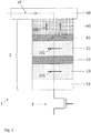
- Fig. 1 representing a magnetic random access memory (MRAM) cell comprising a magnetic tunnel junction.
- MRAM magnetic random access memory
- Fig. 1 represents a magnetic random access memory (MRAM) cell 1 comprising a magnetic tunnel junction 2.
- the magnetic tunnel junction 2 comprises a first ferromagnetic layer 21, a second ferromagnetic layer 23 and an insulating layer, or tunnel barrier layer 22 between the first and second ferromagnetic layers 21, 23.
- the first ferromagnetic layer 21 has a first magnetization 211 having a fixed orientation and the second ferromagnetic layer 23 has a second magnetization 231 that can be freely oriented.
- the first magnetization 211 can be exchange coupled with an anti-ferromagnetic layer (not shown).
- the first ferromagnetic layer 21 and the second ferromagnetic layer 23 are made of 3d metals such as Fe, Co or Ni or their alloys. Eventually, boron can be added in the layer composition in order obtain an amorphous morphology and a flat interface.
- the tunnel barrier layer 22 typically consists of alumina (Al 2 O 3 ) or magnesium oxide (MgO).
- the first ferromagnetic layer 21 can be formed from a synthetic antiferromagnetic layer such as described, for instance, in US Patent No. 5,583,725 .
- the second magnetization 231 can be oriented only in the plane of the layer 23.
- the magnetic tunnel junction 2 further comprises a polarizing layer 60 and a metallic separating layer 61 comprised between the polarizing layer 60 and the first ferromagnetic layer 21.
- the polarizing layer 60 has a perpendicular polarizing magnetization 600, i.e., the polarizing magnetization 600 of the polarizing layer 60 is oriented substantially perpendicular to the plane of the layer 60, or substantially perpendicular to the first and second magnetizations 211, 231.
- the polarizing layer 60 can comprise a stack of layers, made for example of Fe/Pt or Fe/Pd or Co/Pt, or Co/Pd, or Co/Au, etc. or of their alloys, or made of rare-earths /transition metals alloys.
- the magnetic tunnel junction 2 can further comprise a first electrically conductive line, or first electrode 50, and a second electrically conductive line, or second electrode 51, disposed at one end of the magnetic tunnel junction 2, on the side of the polarizing layer 60, and at the other end of the magnetic tunnel junction 2, respectively.
- the MRAM cell 1 can further comprise a switching device, such as a CMOS selecting transistor 3, in electrical communication with one end of the magnetic tunnel junction 2.
- a spin polarized current 32 is passed through the magnetic tunnel junction 2 with a predetermined magnitude such that the second magnetization 231 can be switched.
- the polarizing magnetization 600 of the polarizing layer 60 is oriented substantially perpendicular the first and second magnetizations 211, 231
- the electrons of the spin polarized current 32 are polarized in the polarizing layer 60 with a spin direction perpendicular to the planes of the layers 21, 23.
- the polarized spin electrons of the spin polarized current 32 cause a continuous rotation of the second magnetization 231 within the plane of the second ferromagnetic layer 23.
- the orientation of the second magnetization 231 can be switched when the predetermined magnitude of the spin polarized current 32 is about 1x10 6 A/cm 2 and below.
- a method of forming the magnetic tunnel junction 2 comprises depositing the second electrode 51, the second ferromagnetic layer 23, the tunnel barrier layer 22, and the first ferromagnetic layer 21.
- the method further comprises annealing the deposited ferromagnetic layers 21, 23, i.e., for example, annealing the magnetic tunnel junction 2 comprising the deposited layers 51, 21, 22 and 23, at a first predetermined annealing temperature, adapted to obtain a suitable crystallographic texture of the first and second ferromagnetic layers 21, 23.
- the first predetermined annealing temperature is such that after the annealing step at the first predetermined annealing temperature, the tunnel magnetoresistance of the magnetic tunnel junction 2 is maximal, for example, has a tunnel magnetoresistance value of about 150% and greater.
- the first predetermined annealing temperature is larger than 300°C. In an embodiment, the first predetermined annealing temperature is comprised between about 340°C and 360°C.
- the method further comprises depositing the metallic separating layer 61 and the polarizer layer 60.
- the method further comprises annealing the deposited polarizer layer 60, i.e., annealing the magnetic tunnel junction 2 comprising the deposited polarizer layer 60, at a second predetermined annealing temperature.
- the second predetermined annealing temperature is such as to orient the polarizing magnetization 600 of the polarizer layer 60 substantially perpendicular to the plane of the polarizer layer 60, or substantially perpendicular to the first and second magnetizations 211, 231.
- the second predetermined annealing temperature is lower that the first predetermined annealing temperature.
- the second predetermined annealing temperature is comprised between 150°C and 250°C.
- depositing the first ferromagnetic layer 21, the tunnel barrier layer 22, and the second ferromagnetic layer 23 is performed in this order.
- the magnetic tunnel junction 2 thus manufactured comprises the second ferromagnetic layer 23 between the polarizer layer 60 and the first ferromagnetic layer 21.
- depositing the second ferromagnetic layer 23, the tunnel barrier layer 22, and the first ferromagnetic layer 21, is performed in this order.
- the magnetic tunnel junction 2 thus manufactured comprises the first ferromagnetic layer 21 between the polarizer layer 60 and the second ferromagnetic layer 23.
- a magnetic memory device (not represented) can be formed from an array comprising a plurality of the MRAM cell 1 comprising the magnetic tunnel junction 2 disclosed herein.
- the magnetic tunnel junction 2 manufactured using the method disclosed herein allows for obtaining the magnetic tunnel junction 2 comprising the polarizer layer 60 having its polarizing magnetization 600 substantially perpendicular to the plane of the polarizer layer 60, or substantially perpendicular to the first and second magnetizations 211, 231, and having a high tunnel magnetoresistance.
- the method further allows for minimizing intermixing at the interfaces of the multilayered polarizer layer 60 while the ferromagnetic layers 21, 23 and the tunnel barrier layer 22 are annealed at the high first predetermined annealing temperature, allowing for the high tunnel magnetoresistance to be equal or greater than 150%.
Landscapes
- Engineering & Computer Science (AREA)
- Chemical & Material Sciences (AREA)
- Crystallography & Structural Chemistry (AREA)
- Nanotechnology (AREA)
- Power Engineering (AREA)
- Computer Hardware Design (AREA)
- Physics & Mathematics (AREA)
- Mathematical Physics (AREA)
- Theoretical Computer Science (AREA)
- Hall/Mr Elements (AREA)
- Mram Or Spin Memory Techniques (AREA)
- Magnetic Heads (AREA)
Claims (4)
- Verfahren zur Herstellung eines magnetischen Tunnelübergangs (2), angepasst, um mit einem spinpolarisierten Strom (32) geschrieben zu werden, wobei der magnetische Tunnelübergang (2) umfasst: eine Tunnelbarriereschicht (22) zwischen einer ersten ferromagnetischen Schicht (21) mit einer ersten Magnetisierung (211) von fixer Orientierung und einer zweiten ferromagnetischen Schicht (23) mit einer zweiten Magnetisierung (231) von frei wählbarer Orientierung, und eine Polarisationsschicht (60) mit einer Polarisationsmagnetisierung (600); wobei das Verfahren umfasst:das Abscheiden der ersten ferromagnetischen Schicht (21), der Tunnelbarriereschicht (22) und der zweiten ferromagnetischen Schicht (23);das Tempern der abgeschiedenen ferromagnetischen Schichten (21, 23) bei einer ersten Glühtemperatur von über 300°C, so dass ein Tunnelmagnetowiderstand des magnetischen Tunnelübergangs (2) gleich oder grösser als etwa 150% ist;wobei das Verfahren ferner umfasst:das Abscheiden der Polarisationsschicht (60); unddas Tempern der abgeschiedenen Polarisationsschicht (60) bei einer zweiten Glühtemperatur zwischen 150°C und 250°C, um die Polarisationsmagnetisierung (600) senkrecht zur ersten und zweiten Magnetisierung (211, 231) zu orientieren, worin das besagte Tempern der abgeschiedenen ferromagnetischen Schichten (21, 23) bei der ersten Glühtemperatur vor dem Abscheiden der Polarisationsschicht (60) durchgeführt wird.
- Verfahren gemäss Anspruch 1, worin die erste Glühtemperatur zwischen 340°C und 360°C liegt.
- Verfahren gemäss den Ansprüchen 1 bis 2, worin das Abscheiden der zweiten ferromagnetischen Schicht (23), der Tunnelbarriereschicht (22) und der ersten ferromagnetischen Schicht (21) in dieser Reihenfolge durchgeführt wird.
- Verfahren gemäss irgendeinem der Ansprüche 1 bis 3, worin das Abscheiden der ersten ferromagnetischen Schicht (21), der Tunnelbarriereschicht (22) und der zweiten ferromagnetischen Schicht (23) in dieser Reihenfolge durchgeführt wird.
Priority Applications (6)
| Application Number | Priority Date | Filing Date | Title |
|---|---|---|---|
| EP11290013.9A EP2477227B1 (de) | 2011-01-13 | 2011-01-13 | Magnettunnelübergang mit einer Polarisierungsschicht |
| KR1020120003436A KR20120082359A (ko) | 2011-01-13 | 2012-01-11 | 편광층을 포함하는 자기터널접합 |
| TW101101022A TWI535085B (zh) | 2011-01-13 | 2012-01-11 | 包含極化層之磁性穿隧接面 |
| RU2012101118/08A RU2573756C2 (ru) | 2011-01-13 | 2012-01-12 | Магнитный туннельный переход, содержащий поляризующий слой |
| JP2012003704A JP5903278B2 (ja) | 2011-01-13 | 2012-01-12 | 分極層を備える磁気トンネル接合 |
| US13/348,996 US8609439B2 (en) | 2011-01-13 | 2012-01-12 | Magnetic tunnel junction comprising a polarizing layer |
Applications Claiming Priority (1)
| Application Number | Priority Date | Filing Date | Title |
|---|---|---|---|
| EP11290013.9A EP2477227B1 (de) | 2011-01-13 | 2011-01-13 | Magnettunnelübergang mit einer Polarisierungsschicht |
Publications (2)
| Publication Number | Publication Date |
|---|---|
| EP2477227A1 EP2477227A1 (de) | 2012-07-18 |
| EP2477227B1 true EP2477227B1 (de) | 2019-03-27 |
Family
ID=44246134
Family Applications (1)
| Application Number | Title | Priority Date | Filing Date |
|---|---|---|---|
| EP11290013.9A Active EP2477227B1 (de) | 2011-01-13 | 2011-01-13 | Magnettunnelübergang mit einer Polarisierungsschicht |
Country Status (6)
| Country | Link |
|---|---|
| US (1) | US8609439B2 (de) |
| EP (1) | EP2477227B1 (de) |
| JP (1) | JP5903278B2 (de) |
| KR (1) | KR20120082359A (de) |
| RU (1) | RU2573756C2 (de) |
| TW (1) | TWI535085B (de) |
Families Citing this family (83)
| Publication number | Priority date | Publication date | Assignee | Title |
|---|---|---|---|---|
| EP2479759A1 (de) * | 2011-01-19 | 2012-07-25 | Crocus Technology S.A. | Stromsparende Magnetdirektzugriffsspeicherzelle |
| US9013916B2 (en) * | 2012-05-31 | 2015-04-21 | Northrop Grumman Systems Corporation | Josephson magnetic memory cell system |
| JP6134172B2 (ja) * | 2013-03-21 | 2017-05-24 | 東京エレクトロン株式会社 | 磁気アニール装置 |
| US10297481B2 (en) | 2013-03-21 | 2019-05-21 | Tokyo Electron Limited | Magnetic annealing apparatus |
| US9236560B1 (en) | 2014-12-08 | 2016-01-12 | Western Digital (Fremont), Llc | Spin transfer torque tunneling magnetoresistive device having a laminated free layer with perpendicular magnetic anisotropy |
| US9502642B2 (en) | 2015-04-10 | 2016-11-22 | Micron Technology, Inc. | Magnetic tunnel junctions, methods used while forming magnetic tunnel junctions, and methods of forming magnetic tunnel junctions |
| US9520553B2 (en) | 2015-04-15 | 2016-12-13 | Micron Technology, Inc. | Methods of forming a magnetic electrode of a magnetic tunnel junction and methods of forming a magnetic tunnel junction |
| US9530959B2 (en) | 2015-04-15 | 2016-12-27 | Micron Technology, Inc. | Magnetic tunnel junctions |
| US10468590B2 (en) | 2015-04-21 | 2019-11-05 | Spin Memory, Inc. | High annealing temperature perpendicular magnetic anisotropy structure for magnetic random access memory |
| US9728712B2 (en) | 2015-04-21 | 2017-08-08 | Spin Transfer Technologies, Inc. | Spin transfer torque structure for MRAM devices having a spin current injection capping layer |
| US9257136B1 (en) | 2015-05-05 | 2016-02-09 | Micron Technology, Inc. | Magnetic tunnel junctions |
| US9960346B2 (en) | 2015-05-07 | 2018-05-01 | Micron Technology, Inc. | Magnetic tunnel junctions |
| US9853206B2 (en) | 2015-06-16 | 2017-12-26 | Spin Transfer Technologies, Inc. | Precessional spin current structure for MRAM |
| US9773974B2 (en) | 2015-07-30 | 2017-09-26 | Spin Transfer Technologies, Inc. | Polishing stop layer(s) for processing arrays of semiconductor elements |
| US10163479B2 (en) | 2015-08-14 | 2018-12-25 | Spin Transfer Technologies, Inc. | Method and apparatus for bipolar memory write-verify |
| US9741926B1 (en) | 2016-01-28 | 2017-08-22 | Spin Transfer Technologies, Inc. | Memory cell having magnetic tunnel junction and thermal stability enhancement layer |
| US9680089B1 (en) | 2016-05-13 | 2017-06-13 | Micron Technology, Inc. | Magnetic tunnel junctions |
| US10991410B2 (en) | 2016-09-27 | 2021-04-27 | Spin Memory, Inc. | Bi-polar write scheme |
| US10546625B2 (en) | 2016-09-27 | 2020-01-28 | Spin Memory, Inc. | Method of optimizing write voltage based on error buffer occupancy |
| US10628316B2 (en) | 2016-09-27 | 2020-04-21 | Spin Memory, Inc. | Memory device with a plurality of memory banks where each memory bank is associated with a corresponding memory instruction pipeline and a dynamic redundancy register |
| US10437491B2 (en) | 2016-09-27 | 2019-10-08 | Spin Memory, Inc. | Method of processing incomplete memory operations in a memory device during a power up sequence and a power down sequence using a dynamic redundancy register |
| US10437723B2 (en) | 2016-09-27 | 2019-10-08 | Spin Memory, Inc. | Method of flushing the contents of a dynamic redundancy register to a secure storage area during a power down in a memory device |
| US10360964B2 (en) | 2016-09-27 | 2019-07-23 | Spin Memory, Inc. | Method of writing contents in memory during a power up sequence using a dynamic redundancy register in a memory device |
| US10446210B2 (en) | 2016-09-27 | 2019-10-15 | Spin Memory, Inc. | Memory instruction pipeline with a pre-read stage for a write operation for reducing power consumption in a memory device that uses dynamic redundancy registers |
| US10460781B2 (en) | 2016-09-27 | 2019-10-29 | Spin Memory, Inc. | Memory device with a dual Y-multiplexer structure for performing two simultaneous operations on the same row of a memory bank |
| US11119910B2 (en) | 2016-09-27 | 2021-09-14 | Spin Memory, Inc. | Heuristics for selecting subsegments for entry in and entry out operations in an error cache system with coarse and fine grain segments |
| US11119936B2 (en) | 2016-09-27 | 2021-09-14 | Spin Memory, Inc. | Error cache system with coarse and fine segments for power optimization |
| US11151042B2 (en) | 2016-09-27 | 2021-10-19 | Integrated Silicon Solution, (Cayman) Inc. | Error cache segmentation for power reduction |
| US10366774B2 (en) | 2016-09-27 | 2019-07-30 | Spin Memory, Inc. | Device with dynamic redundancy registers |
| US10818331B2 (en) | 2016-09-27 | 2020-10-27 | Spin Memory, Inc. | Multi-chip module for MRAM devices with levels of dynamic redundancy registers |
| US10672976B2 (en) | 2017-02-28 | 2020-06-02 | Spin Memory, Inc. | Precessional spin current structure with high in-plane magnetization for MRAM |
| US10665777B2 (en) | 2017-02-28 | 2020-05-26 | Spin Memory, Inc. | Precessional spin current structure with non-magnetic insertion layer for MRAM |
| US10032978B1 (en) | 2017-06-27 | 2018-07-24 | Spin Transfer Technologies, Inc. | MRAM with reduced stray magnetic fields |
| US10489245B2 (en) | 2017-10-24 | 2019-11-26 | Spin Memory, Inc. | Forcing stuck bits, waterfall bits, shunt bits and low TMR bits to short during testing and using on-the-fly bit failure detection and bit redundancy remapping techniques to correct them |
| US10529439B2 (en) | 2017-10-24 | 2020-01-07 | Spin Memory, Inc. | On-the-fly bit failure detection and bit redundancy remapping techniques to correct for fixed bit defects |
| US10481976B2 (en) | 2017-10-24 | 2019-11-19 | Spin Memory, Inc. | Forcing bits as bad to widen the window between the distributions of acceptable high and low resistive bits thereby lowering the margin and increasing the speed of the sense amplifiers |
| US10656994B2 (en) | 2017-10-24 | 2020-05-19 | Spin Memory, Inc. | Over-voltage write operation of tunnel magnet-resistance (“TMR”) memory device and correcting failure bits therefrom by using on-the-fly bit failure detection and bit redundancy remapping techniques |
| US10679685B2 (en) | 2017-12-27 | 2020-06-09 | Spin Memory, Inc. | Shared bit line array architecture for magnetoresistive memory |
| US10424726B2 (en) | 2017-12-28 | 2019-09-24 | Spin Memory, Inc. | Process for improving photoresist pillar adhesion during MRAM fabrication |
| US10395712B2 (en) | 2017-12-28 | 2019-08-27 | Spin Memory, Inc. | Memory array with horizontal source line and sacrificial bitline per virtual source |
| US10891997B2 (en) | 2017-12-28 | 2021-01-12 | Spin Memory, Inc. | Memory array with horizontal source line and a virtual source line |
| US10811594B2 (en) | 2017-12-28 | 2020-10-20 | Spin Memory, Inc. | Process for hard mask development for MRAM pillar formation using photolithography |
| US10395711B2 (en) | 2017-12-28 | 2019-08-27 | Spin Memory, Inc. | Perpendicular source and bit lines for an MRAM array |
| US10516094B2 (en) | 2017-12-28 | 2019-12-24 | Spin Memory, Inc. | Process for creating dense pillars using multiple exposures for MRAM fabrication |
| US10360962B1 (en) | 2017-12-28 | 2019-07-23 | Spin Memory, Inc. | Memory array with individually trimmable sense amplifiers |
| US10270027B1 (en) | 2017-12-29 | 2019-04-23 | Spin Memory, Inc. | Self-generating AC current assist in orthogonal STT-MRAM |
| US10236047B1 (en) | 2017-12-29 | 2019-03-19 | Spin Memory, Inc. | Shared oscillator (STNO) for MRAM array write-assist in orthogonal STT-MRAM |
| US10367139B2 (en) | 2017-12-29 | 2019-07-30 | Spin Memory, Inc. | Methods of manufacturing magnetic tunnel junction devices |
| US10199083B1 (en) | 2017-12-29 | 2019-02-05 | Spin Transfer Technologies, Inc. | Three-terminal MRAM with ac write-assist for low read disturb |
| US10360961B1 (en) | 2017-12-29 | 2019-07-23 | Spin Memory, Inc. | AC current pre-charge write-assist in orthogonal STT-MRAM |
| US10546624B2 (en) | 2017-12-29 | 2020-01-28 | Spin Memory, Inc. | Multi-port random access memory |
| US10784439B2 (en) | 2017-12-29 | 2020-09-22 | Spin Memory, Inc. | Precessional spin current magnetic tunnel junction devices and methods of manufacture |
| US10840436B2 (en) | 2017-12-29 | 2020-11-17 | Spin Memory, Inc. | Perpendicular magnetic anisotropy interface tunnel junction devices and methods of manufacture |
| US10424723B2 (en) | 2017-12-29 | 2019-09-24 | Spin Memory, Inc. | Magnetic tunnel junction devices including an optimization layer |
| US10236048B1 (en) | 2017-12-29 | 2019-03-19 | Spin Memory, Inc. | AC current write-assist in orthogonal STT-MRAM |
| US10886330B2 (en) | 2017-12-29 | 2021-01-05 | Spin Memory, Inc. | Memory device having overlapping magnetic tunnel junctions in compliance with a reference pitch |
| US10840439B2 (en) | 2017-12-29 | 2020-11-17 | Spin Memory, Inc. | Magnetic tunnel junction (MTJ) fabrication methods and systems |
| US10255962B1 (en) | 2017-12-30 | 2019-04-09 | Spin Memory, Inc. | Microwave write-assist in orthogonal STT-MRAM |
| US10339993B1 (en) | 2017-12-30 | 2019-07-02 | Spin Memory, Inc. | Perpendicular magnetic tunnel junction device with skyrmionic assist layers for free layer switching |
| US10141499B1 (en) | 2017-12-30 | 2018-11-27 | Spin Transfer Technologies, Inc. | Perpendicular magnetic tunnel junction device with offset precessional spin current layer |
| US10236439B1 (en) | 2017-12-30 | 2019-03-19 | Spin Memory, Inc. | Switching and stability control for perpendicular magnetic tunnel junction device |
| US10319900B1 (en) | 2017-12-30 | 2019-06-11 | Spin Memory, Inc. | Perpendicular magnetic tunnel junction device with precessional spin current layer having a modulated moment density |
| US10229724B1 (en) | 2017-12-30 | 2019-03-12 | Spin Memory, Inc. | Microwave write-assist in series-interconnected orthogonal STT-MRAM devices |
| US10468588B2 (en) | 2018-01-05 | 2019-11-05 | Spin Memory, Inc. | Perpendicular magnetic tunnel junction device with skyrmionic enhancement layers for the precessional spin current magnetic layer |
| US10438995B2 (en) | 2018-01-08 | 2019-10-08 | Spin Memory, Inc. | Devices including magnetic tunnel junctions integrated with selectors |
| US10438996B2 (en) | 2018-01-08 | 2019-10-08 | Spin Memory, Inc. | Methods of fabricating magnetic tunnel junctions integrated with selectors |
| US10388861B1 (en) | 2018-03-08 | 2019-08-20 | Spin Memory, Inc. | Magnetic tunnel junction wafer adaptor used in magnetic annealing furnace and method of using the same |
| US10446744B2 (en) | 2018-03-08 | 2019-10-15 | Spin Memory, Inc. | Magnetic tunnel junction wafer adaptor used in magnetic annealing furnace and method of using the same |
| US11107978B2 (en) | 2018-03-23 | 2021-08-31 | Spin Memory, Inc. | Methods of manufacturing three-dimensional arrays with MTJ devices including a free magnetic trench layer and a planar reference magnetic layer |
| US11107974B2 (en) | 2018-03-23 | 2021-08-31 | Spin Memory, Inc. | Magnetic tunnel junction devices including a free magnetic trench layer and a planar reference magnetic layer |
| US10784437B2 (en) | 2018-03-23 | 2020-09-22 | Spin Memory, Inc. | Three-dimensional arrays with MTJ devices including a free magnetic trench layer and a planar reference magnetic layer |
| US10734573B2 (en) | 2018-03-23 | 2020-08-04 | Spin Memory, Inc. | Three-dimensional arrays with magnetic tunnel junction devices including an annular discontinued free magnetic layer and a planar reference magnetic layer |
| US10411185B1 (en) | 2018-05-30 | 2019-09-10 | Spin Memory, Inc. | Process for creating a high density magnetic tunnel junction array test platform |
| US10559338B2 (en) | 2018-07-06 | 2020-02-11 | Spin Memory, Inc. | Multi-bit cell read-out techniques |
| US10692569B2 (en) | 2018-07-06 | 2020-06-23 | Spin Memory, Inc. | Read-out techniques for multi-bit cells |
| US10600478B2 (en) | 2018-07-06 | 2020-03-24 | Spin Memory, Inc. | Multi-bit cell read-out techniques for MRAM cells with mixed pinned magnetization orientations |
| US10593396B2 (en) | 2018-07-06 | 2020-03-17 | Spin Memory, Inc. | Multi-bit cell read-out techniques for MRAM cells with mixed pinned magnetization orientations |
| US10650875B2 (en) | 2018-08-21 | 2020-05-12 | Spin Memory, Inc. | System for a wide temperature range nonvolatile memory |
| US10699761B2 (en) | 2018-09-18 | 2020-06-30 | Spin Memory, Inc. | Word line decoder memory architecture |
| US10971680B2 (en) | 2018-10-01 | 2021-04-06 | Spin Memory, Inc. | Multi terminal device stack formation methods |
| US11621293B2 (en) | 2018-10-01 | 2023-04-04 | Integrated Silicon Solution, (Cayman) Inc. | Multi terminal device stack systems and methods |
| US10580827B1 (en) | 2018-11-16 | 2020-03-03 | Spin Memory, Inc. | Adjustable stabilizer/polarizer method for MRAM with enhanced stability and efficient switching |
| US11107979B2 (en) | 2018-12-28 | 2021-08-31 | Spin Memory, Inc. | Patterned silicide structures and methods of manufacture |
Family Cites Families (15)
| Publication number | Priority date | Publication date | Assignee | Title |
|---|---|---|---|---|
| US5583725A (en) | 1994-06-15 | 1996-12-10 | International Business Machines Corporation | Spin valve magnetoresistive sensor with self-pinned laminated layer and magnetic recording system using the sensor |
| US5695864A (en) | 1995-09-28 | 1997-12-09 | International Business Machines Corporation | Electronic device using magnetic components |
| US5640343A (en) | 1996-03-18 | 1997-06-17 | International Business Machines Corporation | Magnetic memory array using magnetic tunnel junction devices in the memory cells |
| FR2817999B1 (fr) | 2000-12-07 | 2003-01-10 | Commissariat Energie Atomique | Dispositif magnetique a polarisation de spin et a empilement(s) tri-couche(s) et memoire utilisant ce dispositif |
| JP3908554B2 (ja) * | 2001-07-13 | 2007-04-25 | アルプス電気株式会社 | 磁気検出素子の製造方法 |
| US7270896B2 (en) * | 2004-07-02 | 2007-09-18 | International Business Machines Corporation | High performance magnetic tunnel barriers with amorphous materials |
| JP4682585B2 (ja) * | 2004-11-01 | 2011-05-11 | ソニー株式会社 | 記憶素子及びメモリ |
| JP4575136B2 (ja) * | 2004-12-20 | 2010-11-04 | 株式会社東芝 | 磁気記録素子、磁気記録装置、および情報の記録方法 |
| US7241631B2 (en) * | 2004-12-29 | 2007-07-10 | Grandis, Inc. | MTJ elements with high spin polarization layers configured for spin-transfer switching and spintronics devices using the magnetic elements |
| JP2008028362A (ja) * | 2006-06-22 | 2008-02-07 | Toshiba Corp | 磁気抵抗素子及び磁気メモリ |
| US20070297220A1 (en) * | 2006-06-22 | 2007-12-27 | Masatoshi Yoshikawa | Magnetoresistive element and magnetic memory |
| US7508042B2 (en) * | 2006-12-22 | 2009-03-24 | Magic Technologies, Inc. | Spin transfer MRAM device with magnetic biasing |
| RU2394304C2 (ru) * | 2007-12-26 | 2010-07-10 | Федеральное государственное бюджетное образовательное учреждение высшего профессионального образования "Национальный исследовательский ядерный университет МИФИ" (НИЯУ МИФИ) | Способ формирования структуры магнитного туннельного перехода на основе наноразмерных структур металл-изолятор-металл и структура магнитного туннельного перехода на основе наноразмерных структур металл-изолятор-металл (варианты) |
| WO2009122992A1 (ja) * | 2008-04-03 | 2009-10-08 | 日本電気株式会社 | 磁気抵抗記憶装置 |
| US8957486B2 (en) * | 2009-03-04 | 2015-02-17 | Hitachi, Ltd. | Magnetic memory |
-
2011
- 2011-01-13 EP EP11290013.9A patent/EP2477227B1/de active Active
-
2012
- 2012-01-11 TW TW101101022A patent/TWI535085B/zh not_active IP Right Cessation
- 2012-01-11 KR KR1020120003436A patent/KR20120082359A/ko not_active Withdrawn
- 2012-01-12 US US13/348,996 patent/US8609439B2/en active Active
- 2012-01-12 RU RU2012101118/08A patent/RU2573756C2/ru active
- 2012-01-12 JP JP2012003704A patent/JP5903278B2/ja active Active
Non-Patent Citations (1)
| Title |
|---|
| None * |
Also Published As
| Publication number | Publication date |
|---|---|
| JP2012146984A (ja) | 2012-08-02 |
| US8609439B2 (en) | 2013-12-17 |
| TWI535085B (zh) | 2016-05-21 |
| RU2012101118A (ru) | 2013-07-20 |
| TW201234691A (en) | 2012-08-16 |
| JP5903278B2 (ja) | 2016-04-13 |
| US20120181642A1 (en) | 2012-07-19 |
| KR20120082359A (ko) | 2012-07-23 |
| EP2477227A1 (de) | 2012-07-18 |
| RU2573756C2 (ru) | 2016-01-27 |
Similar Documents
| Publication | Publication Date | Title |
|---|---|---|
| EP2477227B1 (de) | Magnettunnelübergang mit einer Polarisierungsschicht | |
| US11776726B2 (en) | Dipole-coupled spin-orbit torque structure | |
| US8637947B2 (en) | Memory element and memory apparatus | |
| US10217501B2 (en) | Memory element and memory apparatus | |
| USRE49364E1 (en) | Memory element, memory apparatus | |
| US8697484B2 (en) | Method and system for setting a pinned layer in a magnetic tunneling junction | |
| KR20130006375A (ko) | 반-금속성 강자성체들을 이용한 자기 접합을 제공하는 방법 및 시스템 | |
| JP2017139446A (ja) | 改善された切り換え効率のためのスピン軌道トルクビット設計 | |
| US9337416B2 (en) | Memory element and memory apparatus with a plurality of magnetic layers and an oxide layer | |
| WO2014049935A1 (en) | Storage element, storage apparatus, and magnetic head | |
| WO2015064049A1 (en) | Stt mram and magnetic head | |
| EP2528060B1 (de) | Mehrbit-Zelle mit synthetischer Speicherschicht | |
| KR20190104865A (ko) | 자기접합 및 하이브리드 캡핑층을 갖는 자기장치, 이를 이용하는 자기메모리 및 자기장치의 제공방법 | |
| CN103137853A (zh) | 存储元件和存储设备 | |
| EP2249349A1 (de) | Magnetischer Speicher mit wärmeunterstütztem Schreibverfahren und eingeschränktem Schreibfeld | |
| US20130163315A1 (en) | Memory element and memory apparatus | |
| US9472750B2 (en) | Method and system for providing a bottom pinned layer in a perpendicular magnetic junction usable in spin transfer torque magnetic random access memory applications | |
| US9559143B2 (en) | Method and system for providing magnetic junctions including free layers that are cobalt-free |
Legal Events
| Date | Code | Title | Description |
|---|---|---|---|
| PUAI | Public reference made under article 153(3) epc to a published international application that has entered the european phase |
Free format text: ORIGINAL CODE: 0009012 |
|
| AK | Designated contracting states |
Kind code of ref document: A1 Designated state(s): AL AT BE BG CH CY CZ DE DK EE ES FI FR GB GR HR HU IE IS IT LI LT LU LV MC MK MT NL NO PL PT RO RS SE SI SK SM TR |
|
| AX | Request for extension of the european patent |
Extension state: BA ME |
|
| 17P | Request for examination filed |
Effective date: 20130104 |
|
| 17Q | First examination report despatched |
Effective date: 20130603 |
|
| GRAP | Despatch of communication of intention to grant a patent |
Free format text: ORIGINAL CODE: EPIDOSNIGR1 |
|
| STAA | Information on the status of an ep patent application or granted ep patent |
Free format text: STATUS: GRANT OF PATENT IS INTENDED |
|
| INTG | Intention to grant announced |
Effective date: 20181106 |
|
| RIN1 | Information on inventor provided before grant (corrected) |
Inventor name: SOUSA, RICARDO Inventor name: PREJBEANU, IOAN LUCIAN |
|
| GRAS | Grant fee paid |
Free format text: ORIGINAL CODE: EPIDOSNIGR3 |
|
| GRAA | (expected) grant |
Free format text: ORIGINAL CODE: 0009210 |
|
| STAA | Information on the status of an ep patent application or granted ep patent |
Free format text: STATUS: THE PATENT HAS BEEN GRANTED |
|
| AK | Designated contracting states |
Kind code of ref document: B1 Designated state(s): AL AT BE BG CH CY CZ DE DK EE ES FI FR GB GR HR HU IE IS IT LI LT LU LV MC MK MT NL NO PL PT RO RS SE SI SK SM TR |
|
| REG | Reference to a national code |
Ref country code: GB Ref legal event code: FG4D |
|
| REG | Reference to a national code |
Ref country code: CH Ref legal event code: EP |
|
| REG | Reference to a national code |
Ref country code: AT Ref legal event code: REF Ref document number: 1114049 Country of ref document: AT Kind code of ref document: T Effective date: 20190415 |
|
| REG | Reference to a national code |
Ref country code: IE Ref legal event code: FG4D |
|
| REG | Reference to a national code |
Ref country code: DE Ref legal event code: R096 Ref document number: 602011057486 Country of ref document: DE |
|
| PG25 | Lapsed in a contracting state [announced via postgrant information from national office to epo] |
Ref country code: NO Free format text: LAPSE BECAUSE OF FAILURE TO SUBMIT A TRANSLATION OF THE DESCRIPTION OR TO PAY THE FEE WITHIN THE PRESCRIBED TIME-LIMIT Effective date: 20190627 Ref country code: FI Free format text: LAPSE BECAUSE OF FAILURE TO SUBMIT A TRANSLATION OF THE DESCRIPTION OR TO PAY THE FEE WITHIN THE PRESCRIBED TIME-LIMIT Effective date: 20190327 Ref country code: SE Free format text: LAPSE BECAUSE OF FAILURE TO SUBMIT A TRANSLATION OF THE DESCRIPTION OR TO PAY THE FEE WITHIN THE PRESCRIBED TIME-LIMIT Effective date: 20190327 Ref country code: LT Free format text: LAPSE BECAUSE OF FAILURE TO SUBMIT A TRANSLATION OF THE DESCRIPTION OR TO PAY THE FEE WITHIN THE PRESCRIBED TIME-LIMIT Effective date: 20190327 |
|
| REG | Reference to a national code |
Ref country code: NL Ref legal event code: MP Effective date: 20190327 |
|
| PG25 | Lapsed in a contracting state [announced via postgrant information from national office to epo] |
Ref country code: RS Free format text: LAPSE BECAUSE OF FAILURE TO SUBMIT A TRANSLATION OF THE DESCRIPTION OR TO PAY THE FEE WITHIN THE PRESCRIBED TIME-LIMIT Effective date: 20190327 Ref country code: NL Free format text: LAPSE BECAUSE OF FAILURE TO SUBMIT A TRANSLATION OF THE DESCRIPTION OR TO PAY THE FEE WITHIN THE PRESCRIBED TIME-LIMIT Effective date: 20190327 Ref country code: HR Free format text: LAPSE BECAUSE OF FAILURE TO SUBMIT A TRANSLATION OF THE DESCRIPTION OR TO PAY THE FEE WITHIN THE PRESCRIBED TIME-LIMIT Effective date: 20190327 Ref country code: LV Free format text: LAPSE BECAUSE OF FAILURE TO SUBMIT A TRANSLATION OF THE DESCRIPTION OR TO PAY THE FEE WITHIN THE PRESCRIBED TIME-LIMIT Effective date: 20190327 Ref country code: GR Free format text: LAPSE BECAUSE OF FAILURE TO SUBMIT A TRANSLATION OF THE DESCRIPTION OR TO PAY THE FEE WITHIN THE PRESCRIBED TIME-LIMIT Effective date: 20190628 Ref country code: BG Free format text: LAPSE BECAUSE OF FAILURE TO SUBMIT A TRANSLATION OF THE DESCRIPTION OR TO PAY THE FEE WITHIN THE PRESCRIBED TIME-LIMIT Effective date: 20190627 |
|
| REG | Reference to a national code |
Ref country code: AT Ref legal event code: MK05 Ref document number: 1114049 Country of ref document: AT Kind code of ref document: T Effective date: 20190327 |
|
| PG25 | Lapsed in a contracting state [announced via postgrant information from national office to epo] |
Ref country code: EE Free format text: LAPSE BECAUSE OF FAILURE TO SUBMIT A TRANSLATION OF THE DESCRIPTION OR TO PAY THE FEE WITHIN THE PRESCRIBED TIME-LIMIT Effective date: 20190327 Ref country code: RO Free format text: LAPSE BECAUSE OF FAILURE TO SUBMIT A TRANSLATION OF THE DESCRIPTION OR TO PAY THE FEE WITHIN THE PRESCRIBED TIME-LIMIT Effective date: 20190327 Ref country code: IT Free format text: LAPSE BECAUSE OF FAILURE TO SUBMIT A TRANSLATION OF THE DESCRIPTION OR TO PAY THE FEE WITHIN THE PRESCRIBED TIME-LIMIT Effective date: 20190327 Ref country code: AL Free format text: LAPSE BECAUSE OF FAILURE TO SUBMIT A TRANSLATION OF THE DESCRIPTION OR TO PAY THE FEE WITHIN THE PRESCRIBED TIME-LIMIT Effective date: 20190327 Ref country code: CZ Free format text: LAPSE BECAUSE OF FAILURE TO SUBMIT A TRANSLATION OF THE DESCRIPTION OR TO PAY THE FEE WITHIN THE PRESCRIBED TIME-LIMIT Effective date: 20190327 Ref country code: ES Free format text: LAPSE BECAUSE OF FAILURE TO SUBMIT A TRANSLATION OF THE DESCRIPTION OR TO PAY THE FEE WITHIN THE PRESCRIBED TIME-LIMIT Effective date: 20190327 Ref country code: SK Free format text: LAPSE BECAUSE OF FAILURE TO SUBMIT A TRANSLATION OF THE DESCRIPTION OR TO PAY THE FEE WITHIN THE PRESCRIBED TIME-LIMIT Effective date: 20190327 Ref country code: PT Free format text: LAPSE BECAUSE OF FAILURE TO SUBMIT A TRANSLATION OF THE DESCRIPTION OR TO PAY THE FEE WITHIN THE PRESCRIBED TIME-LIMIT Effective date: 20190727 |
|
| PG25 | Lapsed in a contracting state [announced via postgrant information from national office to epo] |
Ref country code: PL Free format text: LAPSE BECAUSE OF FAILURE TO SUBMIT A TRANSLATION OF THE DESCRIPTION OR TO PAY THE FEE WITHIN THE PRESCRIBED TIME-LIMIT Effective date: 20190327 Ref country code: SM Free format text: LAPSE BECAUSE OF FAILURE TO SUBMIT A TRANSLATION OF THE DESCRIPTION OR TO PAY THE FEE WITHIN THE PRESCRIBED TIME-LIMIT Effective date: 20190327 |
|
| PG25 | Lapsed in a contracting state [announced via postgrant information from national office to epo] |
Ref country code: AT Free format text: LAPSE BECAUSE OF FAILURE TO SUBMIT A TRANSLATION OF THE DESCRIPTION OR TO PAY THE FEE WITHIN THE PRESCRIBED TIME-LIMIT Effective date: 20190327 Ref country code: IS Free format text: LAPSE BECAUSE OF FAILURE TO SUBMIT A TRANSLATION OF THE DESCRIPTION OR TO PAY THE FEE WITHIN THE PRESCRIBED TIME-LIMIT Effective date: 20190727 |
|
| REG | Reference to a national code |
Ref country code: DE Ref legal event code: R097 Ref document number: 602011057486 Country of ref document: DE |
|
| PG25 | Lapsed in a contracting state [announced via postgrant information from national office to epo] |
Ref country code: DK Free format text: LAPSE BECAUSE OF FAILURE TO SUBMIT A TRANSLATION OF THE DESCRIPTION OR TO PAY THE FEE WITHIN THE PRESCRIBED TIME-LIMIT Effective date: 20190327 |
|
| PLBE | No opposition filed within time limit |
Free format text: ORIGINAL CODE: 0009261 |
|
| STAA | Information on the status of an ep patent application or granted ep patent |
Free format text: STATUS: NO OPPOSITION FILED WITHIN TIME LIMIT |
|
| PG25 | Lapsed in a contracting state [announced via postgrant information from national office to epo] |
Ref country code: SI Free format text: LAPSE BECAUSE OF FAILURE TO SUBMIT A TRANSLATION OF THE DESCRIPTION OR TO PAY THE FEE WITHIN THE PRESCRIBED TIME-LIMIT Effective date: 20190327 |
|
| 26N | No opposition filed |
Effective date: 20200103 |
|
| REG | Reference to a national code |
Ref country code: DE Ref legal event code: R082 Ref document number: 602011057486 Country of ref document: DE Representative=s name: BECK & ROESSIG EUROPEAN PATENT ATTORNEYS, DE Ref country code: DE Ref legal event code: R082 Ref document number: 602011057486 Country of ref document: DE Representative=s name: BECK & ROESSIG - EUROPEAN PATENT ATTORNEYS, DE |
|
| PG25 | Lapsed in a contracting state [announced via postgrant information from national office to epo] |
Ref country code: TR Free format text: LAPSE BECAUSE OF FAILURE TO SUBMIT A TRANSLATION OF THE DESCRIPTION OR TO PAY THE FEE WITHIN THE PRESCRIBED TIME-LIMIT Effective date: 20190327 |
|
| PG25 | Lapsed in a contracting state [announced via postgrant information from national office to epo] |
Ref country code: MC Free format text: LAPSE BECAUSE OF FAILURE TO SUBMIT A TRANSLATION OF THE DESCRIPTION OR TO PAY THE FEE WITHIN THE PRESCRIBED TIME-LIMIT Effective date: 20190327 |
|
| REG | Reference to a national code |
Ref country code: CH Ref legal event code: PL |
|
| REG | Reference to a national code |
Ref country code: BE Ref legal event code: MM Effective date: 20200131 |
|
| PG25 | Lapsed in a contracting state [announced via postgrant information from national office to epo] |
Ref country code: LU Free format text: LAPSE BECAUSE OF NON-PAYMENT OF DUE FEES Effective date: 20200113 |
|
| PG25 | Lapsed in a contracting state [announced via postgrant information from national office to epo] |
Ref country code: BE Free format text: LAPSE BECAUSE OF NON-PAYMENT OF DUE FEES Effective date: 20200131 Ref country code: LI Free format text: LAPSE BECAUSE OF NON-PAYMENT OF DUE FEES Effective date: 20200131 Ref country code: CH Free format text: LAPSE BECAUSE OF NON-PAYMENT OF DUE FEES Effective date: 20200131 |
|
| PG25 | Lapsed in a contracting state [announced via postgrant information from national office to epo] |
Ref country code: IE Free format text: LAPSE BECAUSE OF NON-PAYMENT OF DUE FEES Effective date: 20200113 |
|
| PG25 | Lapsed in a contracting state [announced via postgrant information from national office to epo] |
Ref country code: MT Free format text: LAPSE BECAUSE OF FAILURE TO SUBMIT A TRANSLATION OF THE DESCRIPTION OR TO PAY THE FEE WITHIN THE PRESCRIBED TIME-LIMIT Effective date: 20190327 Ref country code: CY Free format text: LAPSE BECAUSE OF FAILURE TO SUBMIT A TRANSLATION OF THE DESCRIPTION OR TO PAY THE FEE WITHIN THE PRESCRIBED TIME-LIMIT Effective date: 20190327 |
|
| PG25 | Lapsed in a contracting state [announced via postgrant information from national office to epo] |
Ref country code: MK Free format text: LAPSE BECAUSE OF FAILURE TO SUBMIT A TRANSLATION OF THE DESCRIPTION OR TO PAY THE FEE WITHIN THE PRESCRIBED TIME-LIMIT Effective date: 20190327 |
|
| REG | Reference to a national code |
Ref country code: DE Ref legal event code: R079 Ref document number: 602011057486 Country of ref document: DE Free format text: PREVIOUS MAIN CLASS: H01L0027220000 Ipc: H10B0061000000 |
|
| P01 | Opt-out of the competence of the unified patent court (upc) registered |
Effective date: 20230620 |
|
| REG | Reference to a national code |
Ref country code: DE Ref legal event code: R081 Ref document number: 602011057486 Country of ref document: DE Owner name: CROCUS TECHNOLOGY SA, FR Free format text: FORMER OWNER: CROCUS TECHNOLOGY S.A., GRENOBLE, FR Ref country code: DE Ref legal event code: R081 Ref document number: 602011057486 Country of ref document: DE Owner name: ALLEGRO MICRO SYSTEMS LLC, MANCHESTER, US Free format text: FORMER OWNER: CROCUS TECHNOLOGY S.A., GRENOBLE, FR Ref country code: DE Ref legal event code: R081 Ref document number: 602011057486 Country of ref document: DE Owner name: ALLEGRO MICRO SYSTEMS LLC, WILMINGTON, US Free format text: FORMER OWNER: CROCUS TECHNOLOGY S.A., GRENOBLE, FR |
|
| REG | Reference to a national code |
Ref country code: DE Ref legal event code: R081 Ref document number: 602011057486 Country of ref document: DE Owner name: ALLEGRO MICRO SYSTEMS LLC, MANCHESTER, US Free format text: FORMER OWNER: CROCUS TECHNOLOGY SA, GRENOBLE, FR Ref country code: DE Ref legal event code: R081 Ref document number: 602011057486 Country of ref document: DE Owner name: ALLEGRO MICRO SYSTEMS LLC, WILMINGTON, US Free format text: FORMER OWNER: CROCUS TECHNOLOGY SA, GRENOBLE, FR |
|
| REG | Reference to a national code |
Ref country code: DE Ref legal event code: R081 Ref document number: 602011057486 Country of ref document: DE Owner name: ALLEGRO MICRO SYSTEMS LLC, MANCHESTER, US Free format text: FORMER OWNER: ALLEGRO MICRO SYSTEMS LLC, WILMINGTON, DE, US |
|
| REG | Reference to a national code |
Ref country code: GB Ref legal event code: 732E Free format text: REGISTERED BETWEEN 20240229 AND 20240306 |
|
| PGFP | Annual fee paid to national office [announced via postgrant information from national office to epo] |
Ref country code: GB Payment date: 20241121 Year of fee payment: 15 |
|
| PGFP | Annual fee paid to national office [announced via postgrant information from national office to epo] |
Ref country code: FR Payment date: 20241111 Year of fee payment: 15 |
|
| PGFP | Annual fee paid to national office [announced via postgrant information from national office to epo] |
Ref country code: DE Payment date: 20241120 Year of fee payment: 15 |