EP2485285A2 - Composant à semiconducteur émetteur de lumière et comportant un element de conversion de longueur d'onde - Google Patents
Composant à semiconducteur émetteur de lumière et comportant un element de conversion de longueur d'onde Download PDFInfo
- Publication number
- EP2485285A2 EP2485285A2 EP12166424A EP12166424A EP2485285A2 EP 2485285 A2 EP2485285 A2 EP 2485285A2 EP 12166424 A EP12166424 A EP 12166424A EP 12166424 A EP12166424 A EP 12166424A EP 2485285 A2 EP2485285 A2 EP 2485285A2
- Authority
- EP
- European Patent Office
- Prior art keywords
- recess
- radiation
- conversion element
- emitting semiconductor
- luminescence conversion
- Prior art date
- Legal status (The legal status is an assumption and is not a legal conclusion. Google has not performed a legal analysis and makes no representation as to the accuracy of the status listed.)
- Withdrawn
Links
Images

Classifications
-
- H—ELECTRICITY
- H10—SEMICONDUCTOR DEVICES; ELECTRIC SOLID-STATE DEVICES NOT OTHERWISE PROVIDED FOR
- H10H—INORGANIC LIGHT-EMITTING SEMICONDUCTOR DEVICES HAVING POTENTIAL BARRIERS
- H10H20/00—Individual inorganic light-emitting semiconductor devices having potential barriers, e.g. light-emitting diodes [LED]
- H10H20/80—Constructional details
- H10H20/85—Packages
- H10H20/8506—Containers
-
- H—ELECTRICITY
- H10—SEMICONDUCTOR DEVICES; ELECTRIC SOLID-STATE DEVICES NOT OTHERWISE PROVIDED FOR
- H10H—INORGANIC LIGHT-EMITTING SEMICONDUCTOR DEVICES HAVING POTENTIAL BARRIERS
- H10H20/00—Individual inorganic light-emitting semiconductor devices having potential barriers, e.g. light-emitting diodes [LED]
- H10H20/80—Constructional details
- H10H20/85—Packages
- H10H20/851—Wavelength conversion means
- H10H20/8514—Wavelength conversion means characterised by their shape, e.g. plate or foil
-
- H—ELECTRICITY
- H10—SEMICONDUCTOR DEVICES; ELECTRIC SOLID-STATE DEVICES NOT OTHERWISE PROVIDED FOR
- H10H—INORGANIC LIGHT-EMITTING SEMICONDUCTOR DEVICES HAVING POTENTIAL BARRIERS
- H10H20/00—Individual inorganic light-emitting semiconductor devices having potential barriers, e.g. light-emitting diodes [LED]
- H10H20/01—Manufacture or treatment
- H10H20/036—Manufacture or treatment of packages
- H10H20/0361—Manufacture or treatment of packages of wavelength conversion means
-
- H—ELECTRICITY
- H10—SEMICONDUCTOR DEVICES; ELECTRIC SOLID-STATE DEVICES NOT OTHERWISE PROVIDED FOR
- H10H—INORGANIC LIGHT-EMITTING SEMICONDUCTOR DEVICES HAVING POTENTIAL BARRIERS
- H10H20/00—Individual inorganic light-emitting semiconductor devices having potential barriers, e.g. light-emitting diodes [LED]
- H10H20/80—Constructional details
- H10H20/85—Packages
- H10H20/855—Optical field-shaping means, e.g. lenses
- H10H20/856—Reflecting means
-
- H—ELECTRICITY
- H10—SEMICONDUCTOR DEVICES; ELECTRIC SOLID-STATE DEVICES NOT OTHERWISE PROVIDED FOR
- H10H—INORGANIC LIGHT-EMITTING SEMICONDUCTOR DEVICES HAVING POTENTIAL BARRIERS
- H10H20/00—Individual inorganic light-emitting semiconductor devices having potential barriers, e.g. light-emitting diodes [LED]
- H10H20/80—Constructional details
- H10H20/85—Packages
- H10H20/857—Interconnections, e.g. lead-frames, bond wires or solder balls
-
- H—ELECTRICITY
- H10—SEMICONDUCTOR DEVICES; ELECTRIC SOLID-STATE DEVICES NOT OTHERWISE PROVIDED FOR
- H10W—GENERIC PACKAGES, INTERCONNECTIONS, CONNECTORS OR OTHER CONSTRUCTIONAL DETAILS OF DEVICES COVERED BY CLASS H10
- H10W72/00—Interconnections or connectors in packages
- H10W72/01—Manufacture or treatment
- H10W72/015—Manufacture or treatment of bond wires
- H10W72/01515—Forming coatings
-
- H—ELECTRICITY
- H10—SEMICONDUCTOR DEVICES; ELECTRIC SOLID-STATE DEVICES NOT OTHERWISE PROVIDED FOR
- H10W—GENERIC PACKAGES, INTERCONNECTIONS, CONNECTORS OR OTHER CONSTRUCTIONAL DETAILS OF DEVICES COVERED BY CLASS H10
- H10W72/00—Interconnections or connectors in packages
- H10W72/071—Connecting or disconnecting
- H10W72/075—Connecting or disconnecting of bond wires
-
- H—ELECTRICITY
- H10—SEMICONDUCTOR DEVICES; ELECTRIC SOLID-STATE DEVICES NOT OTHERWISE PROVIDED FOR
- H10W—GENERIC PACKAGES, INTERCONNECTIONS, CONNECTORS OR OTHER CONSTRUCTIONAL DETAILS OF DEVICES COVERED BY CLASS H10
- H10W72/00—Interconnections or connectors in packages
- H10W72/50—Bond wires
- H10W72/531—Shapes of wire connectors
- H10W72/536—Shapes of wire connectors the connected ends being ball-shaped
-
- H—ELECTRICITY
- H10—SEMICONDUCTOR DEVICES; ELECTRIC SOLID-STATE DEVICES NOT OTHERWISE PROVIDED FOR
- H10W—GENERIC PACKAGES, INTERCONNECTIONS, CONNECTORS OR OTHER CONSTRUCTIONAL DETAILS OF DEVICES COVERED BY CLASS H10
- H10W72/00—Interconnections or connectors in packages
- H10W72/50—Bond wires
- H10W72/531—Shapes of wire connectors
- H10W72/5363—Shapes of wire connectors the connected ends being wedge-shaped
-
- H—ELECTRICITY
- H10—SEMICONDUCTOR DEVICES; ELECTRIC SOLID-STATE DEVICES NOT OTHERWISE PROVIDED FOR
- H10W—GENERIC PACKAGES, INTERCONNECTIONS, CONNECTORS OR OTHER CONSTRUCTIONAL DETAILS OF DEVICES COVERED BY CLASS H10
- H10W74/00—Encapsulations, e.g. protective coatings
-
- H—ELECTRICITY
- H10—SEMICONDUCTOR DEVICES; ELECTRIC SOLID-STATE DEVICES NOT OTHERWISE PROVIDED FOR
- H10W—GENERIC PACKAGES, INTERCONNECTIONS, CONNECTORS OR OTHER CONSTRUCTIONAL DETAILS OF DEVICES COVERED BY CLASS H10
- H10W90/00—Package configurations
- H10W90/701—Package configurations characterised by the relative positions of pads or connectors relative to package parts
- H10W90/751—Package configurations characterised by the relative positions of pads or connectors relative to package parts of bond wires
- H10W90/756—Package configurations characterised by the relative positions of pads or connectors relative to package parts of bond wires between a chip and a stacked lead frame, conducting package substrate or heat sink
Definitions
- the invention relates to a radiation-emitting semiconductor component and a production method thereof.
- Radiation-emitting semiconductor devices are made, for example WO 97/50132 known. Such devices include a semiconductor body that emits light in operation (primary light) and a luminescence conversion element that converts a portion of this light into another wavelength range (fluorescent light). The overall color impression of the light emitted by such a semiconductor component results from additive color mixing of primary light and fluorescent light.
- the luminescence conversion element used is a phosphor which is suspended in a synthetic resin.
- a design of radiation-emitting semiconductor components is to arrange the semiconductor body in a recess of the component main body and to fill this recess with the phosphor suspension.
- This arrangement has the disadvantage that the sources of primary light - semiconductor body - and of fluorescent light - phosphor suspension - are generally of different shape and size, so that depending on the radiation splitting takes place in different color components and creates a spatially inhomogeneous color impression. Optical images show strong chromatic errors.
- Another disadvantage is that the color impression of the optical path length in the suspension depends, so that production-related variations in the thickness of the suspension layer above the semiconductor body lead to different color impressions. Furthermore, a very uniform distribution of the phosphor in the suspension is basically necessary.
- the present invention has for its object to develop a radiation-emitting semiconductor device of the type mentioned, which radiates homogeneous mixed-colored light. It is another object of the present invention to provide a manufacturing method for such components.
- the main body of the semiconductor component is designed so that a separate, cup-shaped region is formed in the recess formed for receiving the semiconductor body in the immediate vicinity of the semiconductor body, which contains the luminescence conversion element.
- this arrangement has the advantage that the fluorescent light from almost the same volume as the primary light is emitted, creating a particularly uniform color impression.
- the separate area for receiving the luminescence conversion element is formed by a depression within the recess.
- Another particularly preferred embodiment is to form the separate area by an annular skirt at the bottom of the recess.
- housing with standard shapes can be used as a basic body with great advantage.
- the side surfaces of the recess or the annular enclosure are shaped so that the side surfaces serve as a reflector for the generated radiation and thus the radiation efficiency is increased.
- a lead frame is embedded so that a part of the lead frame forms the bottom surface of the recess in one embodiment described above or that on the lead frame, the annular skirt of the other embodiment described above is formed.
- the semiconductor body is mounted in this development on the lead frame, wherein the electrical contact can be made directly (chip bonding) or by means of wire bonding (wire bonding).
- This so-called ladder frame technique is widely used in radiation-emitting semiconductor devices and can be used with advantage in the present invention.
- the recess may be filled with a radiation-permeable filling compound, for example a potting compound.
- this filler contains a reaction resin, for example an acrylic resin, an epoxy resin, a silicone resin or a mixture of these resins.
- a lens effect or a scattering effect can be achieved which further improves the radiation properties of the component according to the invention or modifies it as desired.
- the luminescence conversion element consists of one or more phosphors, which in a Embedded matrix.
- Acrylic resins, epoxy resins and silicone resins and mixtures thereof are particularly suitable as matrices for miscibility, moldability and handling.
- organic compounds such as, for example, perylene dyes or 4f-organometallic compounds can be mixed in as the phosphor.
- phosphors such as BASF Lumogen F083, Lumogen F240 and Lumogen F300 can be easily added to transparent epoxy resin.
- a white overall color impression can be achieved by using inorganic phosphors.
- Particularly suitable for this purpose are rare earth-doped grenades and rare earth-doped alkaline earth sulfides.
- Efficient phosphors here are compounds which satisfy the formula A 3 B 5 O 12 : M (unless they are unstable under the usual conditions of manufacture and operation).
- A denotes at least one element of the group Y, Lu, Sc, La, Gd, Tb and Sm, B at least one element of the group Al, Ga and In and M at least one element of the group Ce and Pr, preferably Ce.
- YAG Ce (Y 3 Al 5 O 12 : Ce 3+ )
- TbYAG Ce ((Y x Tb 1-x ) 3 Al 5 O 12 : Ce 3+ , 0 ⁇ x ⁇ 1) are particularly preferred here.
- GdYAG Ce ((Gd x Y 1-x ) 3 Al 5 O 12 : Ce 3+ , 0 ⁇ x ⁇ 1)
- GdTbYAG Ce ((Gd x Tb y Y 1-xy ) 3 Al 5 O 12 : Ce 3 , 0 ⁇ x ⁇ 1, 0 ⁇ y ⁇ 1) and mixtures based thereon.
- Al may at least partially be replaced by Ga or In. More preferably, the compounds SrS: Ce 3+ , Na, SrS: Ce 3+ , Cl, SrS: CeCl 3 , CaS: Ce 3+ , SrSe: Ce 3+, and Y 3 Ga 5 O 12 : Ce 3+ .
- rare-earth-doped thiogallates such as, for example, CaGa 2 S 4 : Ce 3+ or SrGa 2 S 4 : Ce 3+ are suitable.
- M ' 2 SiO 5 Ce 3+
- yttrium can be replaced by scandium or lanthanum.
- the particular composition of the phosphor is determined primarily by the desired overall color impression and the central wavelengths of the primary light.
- different materials are used as matrix for the luminescence conversion element and as filling compound in the recess. It can be used with advantage for the luminescence conversion element, a material that is optimal in terms of miscibility with the phosphor and radiation resistance, while a material is selected for the filling material, which is particularly suitable due to its transparency and its mechanical resistance.
- Semiconductor bodies which emit light having a central wavelength of less than 460 nm can be used to particular advantage in devices according to the invention.
- the use of such semiconductor body is not useful in the above-described prior art devices, since light in this wavelength range can damage the filling material, so that the filling material ages very quickly.
- This disadvantage is reduced in the case of components according to the invention, since part of the primary radiation is converted very close to the semiconductor body, so that the proportion of short-wave radiation in the filling compound is reduced and overall the service life of the component is prolonged.
- a silicone resin is used as the matrix for the luminescence conversion element, which is characterized by a particularly high radiation resistance in the green, blue and ultraviolet spectral range.
- the use of silicone resins is particularly advantageous in conjunction with semiconductor bodies that emit radiation having a wavelength below 430 nm. Radiation in this spectral range can cause radiation damage to other resins, significantly reducing the life of the device.
- a luminescence conversion element with a silicone resin matrix can be combined with a filling compound covering the luminescence conversion element based on an epoxy resin.
- Epoxy resins are characterized by high transparency and mechanical stability.
- white light diodes as described in the above-mentioned document WO 97/50132 are described.
- Phosphor and semiconductor body are coordinated so that the colors of primary light and fluorescent light are complementary to each other here. Additive color mixing gives the impression of white light.
- the content of the pamphlets WO 97/50132 and WO 98/12757 becomes the content of this description.
- a plurality of claimed components can be assembled into larger lighting units.
- Such lighting units optionally with matrix-like arrangement of the components, are characterized by high luminance and particularly homogeneous overall color impression.
- the components of the invention are suitable as light sources in imaging lens systems. Since primary and fluorescent light are emitted from spatially closely spaced and approximately equally large volumes, the chromatic distortions that cause such a lens system, are significantly lower than in the light sources according to the above-mentioned prior art. Furthermore, it is therefore advantageously possible, the radiation characteristic of an inventive To modify component by means of one or more lenses without changing the overall color impression.
- Starting point of the manufacturing method according to the invention for a radiation-emitting semiconductor device with Lumineszenzkonversionselement represents a base body with a recess in which a lead frame is embedded, so that a portion of the lead frame forms the bottom surface of the recess.
- the lead frame is over-molded with a molding compound, thereby recessing the chip terminal portion. This recess forms the separate area for receiving the luminescence conversion element.
- the semiconductor body is mounted on the chip terminal region of the lead frame and the necessary for the operation of electrical connections between the semiconductor body and lead frame are made.
- the recessed area is filled with the luminescence conversion element, wherein the semiconductor body is completely embedded in the luminescence conversion element.
- a base body with a recess is also used as the starting product, in which a lead frame is embedded so that a part of the lead frame forms the bottom surface of the recess.
- an annular skirt is formed around the chip terminal region with a molding compound.
- the interior of this enclosure forms the separate area for receiving the luminescence conversion element.
- the semiconductor body is applied to the chip connection region of the leadframe and the electrical connections between semiconductor body and leadframe required for the operation are produced.
- the enclosure is filled with the luminescence conversion element, wherein the semiconductor body is completely embedded in the luminescence conversion element.
- Both methods have the advantage that standard housing or base body with standard housing shapes can be used as the starting material.
- the shape of the separate area for receiving the luminescence conversion element can be easily integrated in the manufacturing process of the device according to the invention.
- the recess is filled with a radiation-permeable filling compound, for example a corresponding potting compound. Since the cladding of the semiconductor body takes place in two steps, advantageously delamination of the semiconductor body from the cladding and crack formation in the cladding is reduced, thereby increasing the moisture resistance and the lifetime of the component.
- a radiation-permeable filling compound for example a corresponding potting compound.
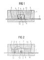
- FIG. 1 shown semiconductor device has a base body 1 a standard housing.
- This may be, for example, a surface-mountable LED housing that consists of a thermoplastic.
- the side walls 5 are slightly bevelled and act as a reflector for the generated radiation.
- a lead frame 2 is integrated.
- the semiconductor body 3 is bonded and electrically connected via a wire connection 4 with the wire terminal portion 11 of the lead frame 2.
- the contacting of the semiconductor body 3 can also take place via a plurality of wire connections.
- the semiconductor body 3 around a smaller reflector ring 6 is formed.
- a material for this reflector ring also a thermoplastic can be used.
- the reflector ring 6 is filled with the luminescence conversion element, which consists of a suspension of the phosphor 8 in a matrix such as silicone. Due to its aging stability, silicone is suitable in particular for the use of short-wave (blue, UV) emitting semiconductor bodies 3.
- the remaining part of the recess is filled with a transparent encapsulation 13 such as epoxy resin.
- the inventive semiconductor device shown differs from that in FIG. 1 shown component in that the area around the semiconductor body 3 for receiving the luminescence conversion element 7 is formed by a recess over the chip terminal region 12 of the lead frame 2.
- the leadframe 2 is covered by a thin molding compound layer 10 (preferably also 0.3 mm to 0.7 mm in height), the depression being formed by a recess of the molding compound layer 10 over the chip connection region 12.
- a thin molding compound layer 10 preferably also 0.3 mm to 0.7 mm in height
- the depression being formed by a recess of the molding compound layer 10 over the chip connection region 12.
- an embodiment of the recess with sharp edges 9 for forming a dome of the luminescence conversion element 7 over the semiconductor body 3 may be advantageous.
- the recessed area of the molding compound around the semiconductor body 3 is filled with the luminescence conversion element 7.
- the wire connection region 11 is recessed from the molding compound layer 10.
- This recess is designed so that the side surfaces of the recess are offset from the housing side surfaces 5. This prevents parts of the phosphor suspension, which can penetrate into the recess above the wire connection region 11 during manufacture, from flowing up to the housing wall 5. This upflow is promoted inter alia by the roughness of the housing wall 5 and is undesirable because it increases the emission range of the fluorescent light.
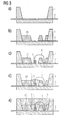
- FIG. 3 schematically an embodiment of a manufacturing method according to the invention is shown.
- the base body 1 is produced with a recess and integrated lead frame 2, FIG. 3a ,
- the lead frame 2 is produced with the housing molding compound in an injection molding process.
- the lead frame 2 is over-molded with the molding compound, for example PPA, so that the lead frame 2 is covered by a molding compound layer 10 of constant thickness.
- the chip connection region 12 and the wire connection region 11 of the leadframe 2 are kept free, FIG. 3b , Alternatively, the in FIG. 3b Of course, shown housing form can also be produced in a single process step.
- the semiconductor body 3 is bonded to the chip connection region 12 and the wire connection 4 is produced between the semiconductor body 3 and the lead frame 2, Figure 3c .
- the recess is filled around the semiconductor body 3 with the luminescence conversion element 7, for example a suspension of a phosphor in a synthetic resin, 3d figure ,
- a potting 13 of the device with a radiation-transparent material such as epoxy resin, FIG. 3e Depending on the requirements of the component, the surface of the casting can be flat, lenticular, studded or run as a diffuser.
- the base body 1 is also produced in the first step with recess and embedded lead frame 2, FIG. 4a ,
- a reflector ring 6 surrounding the chip connection region 12 is sprayed onto the lead frame 2, FIG. 4b , Again, the production of the main body 1 and the reflector ring 6 can be carried out in a single manufacturing step.
- the semiconductor body 3 is then mounted on the chip terminal region 12 of the leadframe 2 and contacted, Figure 4c ,
- the reflector ring 6 is filled with the luminescence conversion element 7 in the form of a phosphor suspension, a dome being formed above the semiconductor body 3 due to the sharp-edged boundary 9 of the reflector ring 6 and the surface tension of the phosphor suspension, FIG. 4d ,
- a complete enclosure of the semiconductor body 3 is ensured without unnecessarily increasing the volume of the luminescence conversion element 7.
- the device can be potted, Figure 4e ,
Landscapes
- Led Device Packages (AREA)
Applications Claiming Priority (2)
| Application Number | Priority Date | Filing Date | Title |
|---|---|---|---|
| DE10020465A DE10020465A1 (de) | 2000-04-26 | 2000-04-26 | Strahlungsemittierendes Halbleiterbauelement mit Lumineszenzkonversionselement |
| EP01940201.5A EP1277242B1 (fr) | 2000-04-26 | 2001-04-26 | Composant a semiconducteurs emettant un rayonnement et comportant un element de conversion luminescent et procede pour sa fabrication |
Related Parent Applications (3)
| Application Number | Title | Priority Date | Filing Date |
|---|---|---|---|
| EP01940201.5A Division-Into EP1277242B1 (fr) | 2000-04-26 | 2001-04-26 | Composant a semiconducteurs emettant un rayonnement et comportant un element de conversion luminescent et procede pour sa fabrication |
| EP01940201.5A Division EP1277242B1 (fr) | 2000-04-26 | 2001-04-26 | Composant a semiconducteurs emettant un rayonnement et comportant un element de conversion luminescent et procede pour sa fabrication |
| EP01940201.5 Division | 2001-04-26 |
Publications (2)
| Publication Number | Publication Date |
|---|---|
| EP2485285A2 true EP2485285A2 (fr) | 2012-08-08 |
| EP2485285A3 EP2485285A3 (fr) | 2015-09-16 |
Family
ID=7640000
Family Applications (2)
| Application Number | Title | Priority Date | Filing Date |
|---|---|---|---|
| EP12166424.7A Withdrawn EP2485285A3 (fr) | 2000-04-26 | 2001-04-26 | Composant à semiconducteur émetteur de lumière et comportant un element de conversion de longueur d'onde |
| EP01940201.5A Expired - Lifetime EP1277242B1 (fr) | 2000-04-26 | 2001-04-26 | Composant a semiconducteurs emettant un rayonnement et comportant un element de conversion luminescent et procede pour sa fabrication |
Family Applications After (1)
| Application Number | Title | Priority Date | Filing Date |
|---|---|---|---|
| EP01940201.5A Expired - Lifetime EP1277242B1 (fr) | 2000-04-26 | 2001-04-26 | Composant a semiconducteurs emettant un rayonnement et comportant un element de conversion luminescent et procede pour sa fabrication |
Country Status (7)
| Country | Link |
|---|---|
| US (3) | US6897490B2 (fr) |
| EP (2) | EP2485285A3 (fr) |
| JP (2) | JP5100944B2 (fr) |
| CN (2) | CN1284249C (fr) |
| DE (1) | DE10020465A1 (fr) |
| TW (1) | TW533602B (fr) |
| WO (1) | WO2001082385A1 (fr) |
Cited By (1)
| Publication number | Priority date | Publication date | Assignee | Title |
|---|---|---|---|---|
| EP2054949B1 (fr) * | 2006-12-19 | 2017-01-25 | OSRAM Opto Semiconductors GmbH | Composant semi-conducteur optoélectronique |
Families Citing this family (138)
| Publication number | Priority date | Publication date | Assignee | Title |
|---|---|---|---|---|
| EP1471775B9 (fr) * | 1999-07-23 | 2011-04-13 | OSRAM Opto Semiconductors GmbH | Source lumineuse avec un dispositif incluant une substance lumineuse et matière moulable contenant un arrangement d'une substance lumineuse |
| JP4817534B2 (ja) * | 2000-06-09 | 2011-11-16 | 星和電機株式会社 | 発光ダイオードランプ |
| DE10122002A1 (de) * | 2001-05-07 | 2002-11-21 | Osram Opto Semiconductors Gmbh | Gehäuse für ein optoelektronisches Bauelement und optoelektronisches Bauelement |
| US6616862B2 (en) | 2001-05-21 | 2003-09-09 | General Electric Company | Yellow light-emitting halophosphate phosphors and light sources incorporating the same |
| US6596195B2 (en) * | 2001-06-01 | 2003-07-22 | General Electric Company | Broad-spectrum terbium-containing garnet phosphors and white-light sources incorporating the same |
| DE10214119A1 (de) * | 2002-03-28 | 2003-10-23 | Osram Opto Semiconductors Gmbh | Optoelektronisches Bauelement |
| WO2004001862A1 (fr) * | 2002-06-19 | 2003-12-31 | Sanken Electric Co., Ltd. | Dispositif electroluminescent a semi-conducteurs, procede de production de ce dispositif et reflecteur concu pour un dispositif electroluminescent a semi-conducteurs |
| TW200414572A (en) | 2002-11-07 | 2004-08-01 | Matsushita Electric Industrial Co Ltd | LED lamp |
| US7595113B2 (en) | 2002-11-29 | 2009-09-29 | Shin-Etsu Chemical Co., Ltd. | LED devices and silicone resin composition therefor |
| JP2004186168A (ja) * | 2002-11-29 | 2004-07-02 | Shin Etsu Chem Co Ltd | 発光ダイオード素子用シリコーン樹脂組成物 |
| DE20306928U1 (de) * | 2003-01-30 | 2004-06-03 | Osram Opto Semiconductors Gmbh | Elektromagnetische Strahlung aussendendes und/oder empfangendes Halbleiter-Bauelement und Gehäuse-Grundkörper für ein derartiges Bauelement |
| TWI237546B (en) | 2003-01-30 | 2005-08-01 | Osram Opto Semiconductors Gmbh | Semiconductor-component sending and/or receiving electromagnetic radiation and housing-basebody for such a component |
| JP2004260620A (ja) | 2003-02-26 | 2004-09-16 | Ntt Docomo Inc | 無線データ通信方法、サーバ装置及び無線制御装置 |
| JP2004265979A (ja) * | 2003-02-28 | 2004-09-24 | Noritsu Koki Co Ltd | 発光ダイオード光源ユニット |
| CN100379041C (zh) | 2003-08-07 | 2008-04-02 | 松下电器产业株式会社 | Led照明光源及其制造方法 |
| BRPI0413558A (pt) | 2003-08-12 | 2006-10-17 | 3M Innovative Properties Co | compostos contendo imidazo substituìdo por hidroxilamina |
| AU2004268625B2 (en) | 2003-08-27 | 2011-03-31 | 3M Innovative Properties Company | Aryloxy and arylalkyleneoxy substituted imidazoquinolines |
| AU2004270201A1 (en) | 2003-09-05 | 2005-03-17 | 3M Innovative Properties Company | Treatment for CD5+ B cell lymphoma |
| US7854535B2 (en) | 2003-09-23 | 2010-12-21 | Avago Technologies Ecbu Ip (Singapore) Pte. Ltd. | Ceramic packaging for high brightness LED devices |
| US20080025030A9 (en) * | 2003-09-23 | 2008-01-31 | Lee Kong W | Ceramic packaging for high brightness LED devices |
| US7544697B2 (en) | 2003-10-03 | 2009-06-09 | Coley Pharmaceutical Group, Inc. | Pyrazolopyridines and analogs thereof |
| AR046046A1 (es) | 2003-10-03 | 2005-11-23 | 3M Innovative Properties Co | Imidazoquinolinas alcoxi sustituidas. composiciones farmaceuticas. |
| CA2545825A1 (fr) | 2003-11-14 | 2005-06-02 | 3M Innovative Properties Company | Composes d'un anneau d'imidazo substitue par hydroxylamine |
| EP1685129A4 (fr) | 2003-11-14 | 2008-10-22 | 3M Innovative Properties Co | Composes d'un anneau d'imidazo substitues par oxime |
| CA2547020C (fr) | 2003-11-25 | 2014-03-25 | 3M Innovative Properties Company | Derives de 1h-imidazo[4,5-c]pyridine-4-amine en tant que compose modificateur de la reponse immunitaire |
| JP2007517035A (ja) | 2003-12-29 | 2007-06-28 | スリーエム イノベイティブ プロパティズ カンパニー | アリールアルケニルおよびアリールアルキニル置換されたイミダゾキノリン |
| EP1699788A2 (fr) | 2003-12-30 | 2006-09-13 | 3M Innovative Properties Company | Sulfonamides d'imidazoquinolinyle, d'imidazopyridinyle et d'imidazonaphtyridinyle |
| JP2005223112A (ja) * | 2004-02-05 | 2005-08-18 | Citizen Electronics Co Ltd | 表面実装型発光ダイオード |
| CN100391020C (zh) | 2004-02-26 | 2008-05-28 | 松下电器产业株式会社 | Led光源 |
| WO2005094531A2 (fr) | 2004-03-24 | 2005-10-13 | 3M Innovative Properties Company | Imidazopyridines, imidazoquinolines, et imidazonaphthyridines a substitution amide |
| JP4754850B2 (ja) * | 2004-03-26 | 2011-08-24 | パナソニック株式会社 | Led実装用モジュールの製造方法及びledモジュールの製造方法 |
| US7279346B2 (en) * | 2004-03-31 | 2007-10-09 | Cree, Inc. | Method for packaging a light emitting device by one dispense then cure step followed by another |
| US7517728B2 (en) | 2004-03-31 | 2009-04-14 | Cree, Inc. | Semiconductor light emitting devices including a luminescent conversion element |
| US7326583B2 (en) * | 2004-03-31 | 2008-02-05 | Cree, Inc. | Methods for packaging of a semiconductor light emitting device |
| DE102004021233A1 (de) | 2004-04-30 | 2005-12-01 | Osram Opto Semiconductors Gmbh | Leuchtdiodenanordnung |
| WO2005117071A2 (fr) | 2004-05-31 | 2005-12-08 | Osram Opto Semiconductors Gmbh | Composant optoelectronique a semi-conducteur et corps de base de boitier pour un tel composant |
| US8017779B2 (en) | 2004-06-15 | 2011-09-13 | 3M Innovative Properties Company | Nitrogen containing heterocyclyl substituted imidazoquinolines and imidazonaphthyridines |
| WO2006038923A2 (fr) | 2004-06-18 | 2006-04-13 | 3M Innovative Properties Company | Imidazonaphthyridines substituees par aryle |
| US8026366B2 (en) | 2004-06-18 | 2011-09-27 | 3M Innovative Properties Company | Aryloxy and arylalkyleneoxy substituted thiazoloquinolines and thiazolonaphthyridines |
| WO2006065280A2 (fr) | 2004-06-18 | 2006-06-22 | 3M Innovative Properties Company | Composes a noyau imidazo a substitutif d'isoxazole, de dihydroisoxazole et d'oxadiazole |
| EP1622237A1 (fr) * | 2004-07-28 | 2006-02-01 | Infineon Technologies Fiber Optics GmbH | Module électronique ou optique et méthode implémentée par ledit module |
| US20060038198A1 (en) * | 2004-08-23 | 2006-02-23 | Chua Janet B Y | Device and method for producing output light having a wavelength spectrum in the visible range and the infrared range using a fluorescent material |
| EP1630913B1 (fr) * | 2004-08-31 | 2007-10-03 | Infineon Technologies AG | Méthode de fabrication d'un module électronique ou optique dans un boîtier en matière plastique contenant un composant électronique ou optique ainsi que ledit module optique ou électronique |
| DE102004047640A1 (de) * | 2004-09-30 | 2006-04-13 | Osram Opto Semiconductors Gmbh | Optoelektronisches Bauelement und Gehäuse für ein optoelektronisches Bauelement |
| US7679672B2 (en) * | 2004-10-14 | 2010-03-16 | Avago Technologies Ecbu Ip (Singapore) Pte. Ltd. | Electronic flash, imaging device and method for producing a flash of light having a wavelength spectrum in the visible range and the infrared range using a fluorescent material |
| US20060082995A1 (en) * | 2004-10-14 | 2006-04-20 | Chua Janet B Y | Device and method for producing output light having a wavelength spectrum in the infrared wavelength range and the visble wavelength range |
| DE102004053116A1 (de) | 2004-11-03 | 2006-05-04 | Tridonic Optoelectronics Gmbh | Leuchtdioden-Anordnung mit Farbkonversions-Material |
| JP5543068B2 (ja) | 2004-12-30 | 2014-07-09 | スリーエム イノベイティブ プロパティズ カンパニー | キラル縮合[1,2]イミダゾ[4,5−c]環状化合物 |
| EP1831221B1 (fr) | 2004-12-30 | 2012-08-08 | 3M Innovative Properties Company | Composes chiraux 1,2 imidazo 4,5-c substitues a noyau fusionne |
| KR101047795B1 (ko) * | 2005-01-05 | 2011-07-07 | 엘지이노텍 주식회사 | 반도체 발광소자 |
| US7939842B2 (en) | 2005-01-27 | 2011-05-10 | Cree, Inc. | Light emitting device packages, light emitting diode (LED) packages and related methods |
| AU2006210392A1 (en) | 2005-02-04 | 2006-08-10 | Coley Pharmaceutical Group, Inc. | Aqueous gel formulations containing immune response modifiers |
| AU2006213746A1 (en) | 2005-02-11 | 2006-08-17 | Coley Pharmaceutical Group, Inc. | Oxime and hydroxylamine substituted imidazo(4,5-c) ring compounds and methods |
| CN100377376C (zh) * | 2005-03-21 | 2008-03-26 | 亿光电子工业股份有限公司 | 发光二极管反射盖制造方法 |
| DE112006000694B4 (de) * | 2005-03-24 | 2013-10-17 | Kyocera Corp. | Gehäuse für Lichtemissionsvorrichtung, lichtemittierende Vorrichtung und Beleuchtungsvorrichtung |
| AU2006232375A1 (en) | 2005-04-01 | 2006-10-12 | Coley Pharmaceutical Group, Inc. | 1-substituted pyrazolo (3,4-c) ring compounds as modulators of cytokine biosynthesis for the treatment of viral infections and neoplastic diseases |
| EP1869043A2 (fr) | 2005-04-01 | 2007-12-26 | Coley Pharmaceutical Group, Inc. | Pyrazolopyridine-1,4-diamines et analogues associes |
| KR100631993B1 (ko) * | 2005-07-20 | 2006-10-09 | 삼성전기주식회사 | Led 패키지 및 그 제조방법 |
| US7646035B2 (en) * | 2006-05-31 | 2010-01-12 | Cree, Inc. | Packaged light emitting devices including multiple index lenses and multiple index lenses for packaged light emitting devices |
| US7365371B2 (en) * | 2005-08-04 | 2008-04-29 | Cree, Inc. | Packages for semiconductor light emitting devices utilizing dispensed encapsulants |
| US8835952B2 (en) | 2005-08-04 | 2014-09-16 | Cree, Inc. | Submounts for semiconductor light emitting devices and methods of forming packaged light emitting devices including dispensed encapsulants |
| US20070045800A1 (en) * | 2005-08-19 | 2007-03-01 | Brian King | Opto-coupler with high reverse breakdown voltage and high isolation potential |
| KR100780176B1 (ko) * | 2005-11-25 | 2007-11-27 | 삼성전기주식회사 | 측면 방출 발광다이오드 패키지 |
| WO2007081719A2 (fr) | 2006-01-05 | 2007-07-19 | Illumitex, Inc. | Dispositif optique séparé pour diriger de la lumière depuis une del |
| US8044412B2 (en) | 2006-01-20 | 2011-10-25 | Taiwan Semiconductor Manufacturing Company, Ltd | Package for a light emitting element |
| TWI331815B (en) | 2006-03-17 | 2010-10-11 | Seoul Semiconductor Co Ltd | Side-view light emitting diode package having a reflector |
| KR100875443B1 (ko) | 2006-03-31 | 2008-12-23 | 서울반도체 주식회사 | 발광 장치 |
| US8969908B2 (en) * | 2006-04-04 | 2015-03-03 | Cree, Inc. | Uniform emission LED package |
| US20070269915A1 (en) * | 2006-05-16 | 2007-11-22 | Ak Wing Leong | LED devices incorporating moisture-resistant seals and having ceramic substrates |
| US20070272934A1 (en) * | 2006-05-23 | 2007-11-29 | Kee Yean Ng | LED device with improved life performance |
| WO2007139894A2 (fr) | 2006-05-26 | 2007-12-06 | Cree Led Lighting Solutions, Inc. | Dispositif électroluminescent à semi-conducteurs et procédé de fabrication correspondant |
| US7906506B2 (en) | 2006-07-12 | 2011-03-15 | 3M Innovative Properties Company | Substituted chiral fused [1,2] imidazo [4,5-c] ring compounds and methods |
| TWI418054B (zh) * | 2006-08-08 | 2013-12-01 | Lg電子股份有限公司 | 發光裝置封裝與製造此封裝之方法 |
| US8367945B2 (en) * | 2006-08-16 | 2013-02-05 | Cree Huizhou Opto Limited | Apparatus, system and method for use in mounting electronic elements |
| DE102006046301A1 (de) * | 2006-09-29 | 2008-04-03 | Osram Opto Semiconductors Gmbh | Optisches Element, strahlungsemittierendes Bauelement und Verfahren zur Herstellung eines optischen Elements |
| DE102006046678A1 (de) * | 2006-09-29 | 2008-04-03 | Osram Opto Semiconductors Gmbh | Gehäuse für ein optoelektronisches Bauelement, optoelektronisches Bauelement und Verfahren zum Herstellen eines Gehäuses für ein optoelektronisches Bauelement |
| US8087960B2 (en) | 2006-10-02 | 2012-01-03 | Illumitex, Inc. | LED system and method |
| US7808013B2 (en) * | 2006-10-31 | 2010-10-05 | Cree, Inc. | Integrated heat spreaders for light emitting devices (LEDs) and related assemblies |
| TWI326923B (en) * | 2007-03-07 | 2010-07-01 | Lite On Technology Corp | White light emitting diode |
| JP2008277607A (ja) * | 2007-05-01 | 2008-11-13 | Matsushita Electric Ind Co Ltd | 発光装置、線状発光装置、面状発光装置、液晶表示装置および電子機器 |
| US7915061B2 (en) * | 2007-05-31 | 2011-03-29 | GE Lighting Solutions, LLC | Environmentally robust lighting devices and methods of manufacturing same |
| US10505083B2 (en) * | 2007-07-11 | 2019-12-10 | Cree, Inc. | Coating method utilizing phosphor containment structure and devices fabricated using same |
| US9401461B2 (en) * | 2007-07-11 | 2016-07-26 | Cree, Inc. | LED chip design for white conversion |
| JP2009021426A (ja) * | 2007-07-12 | 2009-01-29 | Sharp Corp | チップ部品型led及びその製造方法 |
| DE102007042642A1 (de) * | 2007-09-07 | 2009-03-12 | Osram Gesellschaft mit beschränkter Haftung | Verfahren zum Herstellen eines optoelektronischen Bauelements und optoelektronisches Bauelement |
| US10256385B2 (en) | 2007-10-31 | 2019-04-09 | Cree, Inc. | Light emitting die (LED) packages and related methods |
| US7687252B2 (en) * | 2007-11-05 | 2010-03-30 | Hauptman-Woodward Medcial Research Institute, Inc. | Protein crystal of human cytochrome P450 aromatase and uses thereof |
| DE102008003971A1 (de) * | 2008-01-11 | 2009-07-16 | Ledon Lighting Jennersdorf Gmbh | Leuchtdiodenanordnung mit Schutzrahmen |
| JP2011512037A (ja) | 2008-02-08 | 2011-04-14 | イルミテックス, インコーポレイテッド | エミッタ層成形のためのシステムおよび方法 |
| US8877524B2 (en) * | 2008-03-31 | 2014-11-04 | Cree, Inc. | Emission tuning methods and devices fabricated utilizing methods |
| JP5207807B2 (ja) * | 2008-04-14 | 2013-06-12 | シャープ株式会社 | チップ部品型led |
| CN101577300A (zh) * | 2008-05-08 | 2009-11-11 | 先进开发光电股份有限公司 | 发光二极管及其封装方法 |
| TWI475718B (zh) * | 2008-05-21 | 2015-03-01 | 榮創能源科技股份有限公司 | 發光二極體及其封裝方法 |
| US20100067240A1 (en) * | 2008-09-16 | 2010-03-18 | John Selverian | Optical Cup For Lighting Module |
| US8188486B2 (en) * | 2008-09-16 | 2012-05-29 | Osram Sylvania Inc. | Optical disk for lighting module |
| US8183585B2 (en) * | 2008-09-16 | 2012-05-22 | Osram Sylvania Inc. | Lighting module |
| US8022626B2 (en) * | 2008-09-16 | 2011-09-20 | Osram Sylvania Inc. | Lighting module |
| JP2010123746A (ja) * | 2008-11-19 | 2010-06-03 | Toshiba Corp | 光半導体装置と、照明装置および表示装置 |
| JP4799606B2 (ja) * | 2008-12-08 | 2011-10-26 | 株式会社東芝 | 光半導体装置及び光半導体装置の製造方法 |
| TW201034256A (en) | 2008-12-11 | 2010-09-16 | Illumitex Inc | Systems and methods for packaging light-emitting diode devices |
| TWI403006B (zh) | 2009-01-15 | 2013-07-21 | 億光電子工業股份有限公司 | 發光二極體元件封裝結構及其製造方法 |
| TWI449221B (zh) * | 2009-01-16 | 2014-08-11 | 億光電子工業股份有限公司 | 發光二極體封裝結構及其製造方法 |
| CN101783379B (zh) * | 2009-01-20 | 2011-08-24 | 亿光电子工业股份有限公司 | 发光二极管元件封装结构及其制造方法 |
| US8449128B2 (en) | 2009-08-20 | 2013-05-28 | Illumitex, Inc. | System and method for a lens and phosphor layer |
| US8585253B2 (en) | 2009-08-20 | 2013-11-19 | Illumitex, Inc. | System and method for color mixing lens array |
| DE102009055786A1 (de) * | 2009-11-25 | 2011-05-26 | Osram Opto Semiconductors Gmbh | Gehäuse, optoelektronisches Bauteil und Verfahren zur Herstellung eines Gehäuses |
| TW201128812A (en) * | 2009-12-01 | 2011-08-16 | Lg Innotek Co Ltd | Light emitting device |
| JP5535750B2 (ja) * | 2010-04-30 | 2014-07-02 | ローム株式会社 | 発光素子モジュール |
| KR101039994B1 (ko) | 2010-05-24 | 2011-06-09 | 엘지이노텍 주식회사 | 발광소자 및 이를 구비한 라이트 유닛 |
| CN101859759A (zh) * | 2010-06-03 | 2010-10-13 | 陕西科技大学 | 一种白色led光源封装 |
| US9033530B2 (en) | 2010-06-22 | 2015-05-19 | Osram Gmbh | Phosphor device and lighting apparatus comprising the same |
| KR101677105B1 (ko) * | 2010-08-30 | 2016-11-17 | 삼성디스플레이 주식회사 | 전자 부품 및 그 제조 방법 |
| KR101761637B1 (ko) * | 2010-11-24 | 2017-07-27 | 삼성전자주식회사 | 발광 다이오드 패키지 및 그의 제조 방법 |
| JP2014038876A (ja) * | 2010-12-15 | 2014-02-27 | Panasonic Corp | 半導体発光装置 |
| JP5582048B2 (ja) * | 2011-01-28 | 2014-09-03 | 日亜化学工業株式会社 | 発光装置 |
| KR101847938B1 (ko) * | 2011-03-14 | 2018-04-13 | 삼성전자주식회사 | 발광소자 패키지 및 그 제조 방법 |
| CN102694102B (zh) * | 2011-03-22 | 2014-11-05 | 展晶科技(深圳)有限公司 | 发光二极管封装结构及其制造方法、以及光源装置 |
| JP5962102B2 (ja) * | 2011-03-24 | 2016-08-03 | 日亜化学工業株式会社 | 発光装置及びその製造方法 |
| JP5643700B2 (ja) * | 2011-03-29 | 2014-12-17 | シャープ株式会社 | 配線基板の加工方法及びその製造方法、発光装置及びその製造方法、並びに電気機器 |
| JP2012209291A (ja) * | 2011-03-29 | 2012-10-25 | Citizen Electronics Co Ltd | 発光ダイオード |
| CN108565329A (zh) * | 2011-11-17 | 2018-09-21 | 株式会社流明斯 | 发光元件封装体以及包括该发光元件封装体的背光单元 |
| US20130249387A1 (en) * | 2012-03-20 | 2013-09-26 | Chia-Fen Hsin | Light-emitting diodes, packages, and methods of making |
| WO2013152362A1 (fr) * | 2012-04-07 | 2013-10-10 | Axlen, Inc. | Dispositifs d'éclairage à del à grand flux et haute luminosité |
| CN103489984B (zh) * | 2012-06-13 | 2017-09-12 | 亿光电子工业股份有限公司 | 发光二极管封装结构及其制作方法 |
| JP6476567B2 (ja) | 2013-03-29 | 2019-03-06 | 日亜化学工業株式会社 | 発光装置 |
| DE102013206186A1 (de) | 2013-04-09 | 2014-10-09 | Osram Opto Semiconductors Gmbh | Optoelektronisches Bauelement |
| DE102013213073A1 (de) * | 2013-07-04 | 2015-01-08 | Osram Opto Semiconductors Gmbh | Verfahren zum Herstellen eines optoelektronischen Bauelementes |
| CN103390718B (zh) * | 2013-08-07 | 2016-01-20 | 昆山亿业嘉精密机械有限公司 | 一种带球led封装上模成型工艺及其封装方法 |
| JP6255884B2 (ja) * | 2013-10-16 | 2018-01-10 | 大日本印刷株式会社 | 光半導体装置、光半導体装置用リードフレーム、及びそれらの製造方法 |
| JP6229455B2 (ja) * | 2013-11-25 | 2017-11-15 | 日亜化学工業株式会社 | 発光装置及びその製造方法 |
| US20160079217A1 (en) * | 2014-09-12 | 2016-03-17 | Kabushiki Kaisha Toshiba | Semiconductor light emitting device and lead frame |
| DE102014117435A1 (de) * | 2014-11-27 | 2016-06-02 | Osram Opto Semiconductors Gmbh | Bauteil mit Leiterrahmenabschnitt |
| US9991689B2 (en) * | 2015-12-16 | 2018-06-05 | Eaton Intelligent Power Limited | Power pedestal and mounting assembly therefor |
| JP6837776B2 (ja) * | 2016-08-10 | 2021-03-03 | 株式会社小糸製作所 | 車両用前照灯 |
| CN109891274B (zh) * | 2016-10-28 | 2021-09-24 | 日本特殊陶业株式会社 | 光波长转换部件及发光装置 |
| JP7011143B2 (ja) * | 2016-11-30 | 2022-01-26 | 日亜化学工業株式会社 | 発光装置の製造方法 |
| CN110391326A (zh) * | 2018-04-17 | 2019-10-29 | 展晶科技(深圳)有限公司 | 侧面发光型发光二极管封装结构 |
| CN112430126B (zh) * | 2020-11-26 | 2022-08-30 | 中国计量大学 | 一种激光激发荧光玻璃膜及其制备方法 |
Citations (2)
| Publication number | Priority date | Publication date | Assignee | Title |
|---|---|---|---|---|
| WO1997050132A1 (fr) | 1996-06-26 | 1997-12-31 | Siemens Aktiengesellschaft | Composant a semi-conducteur luminescent avec element de conversion de la luminescence |
| WO1998012757A1 (fr) | 1996-09-20 | 1998-03-26 | Siemens Aktiengesellschaft | Masse de scellement a effet convertisseur de longueur d'onde, utilisation et procede de production |
Family Cites Families (24)
| Publication number | Priority date | Publication date | Assignee | Title |
|---|---|---|---|---|
| JPS48102585A (fr) * | 1972-04-04 | 1973-12-22 | ||
| JPS5856483A (ja) * | 1981-09-30 | 1983-04-04 | Toshiba Corp | 光半導体装置 |
| EP1022787B2 (fr) | 1989-05-31 | 2012-07-11 | OSRAM Opto Semiconductors GmbH | Procédé de production d'un élément optique fixable sur une surface et élément optique fixable sur une surface |
| JPH0343750U (fr) * | 1989-09-04 | 1991-04-24 | ||
| JPH0440554U (fr) * | 1990-07-31 | 1992-04-07 | ||
| JPH05190908A (ja) * | 1992-01-13 | 1993-07-30 | Nec Corp | 光電変換装置 |
| JPH0927643A (ja) | 1995-07-13 | 1997-01-28 | Stanley Electric Co Ltd | 受光/発光素子 |
| JP3832877B2 (ja) * | 1995-07-26 | 2006-10-11 | 日亜化学工業株式会社 | セラミックスledパッケージおよびその製造方法 |
| DE19549818B4 (de) * | 1995-09-29 | 2010-03-18 | Osram Opto Semiconductors Gmbh | Optoelektronisches Halbleiter-Bauelement |
| TW383508B (en) | 1996-07-29 | 2000-03-01 | Nichia Kagaku Kogyo Kk | Light emitting device and display |
| JP3065258B2 (ja) * | 1996-09-30 | 2000-07-17 | 日亜化学工業株式会社 | 発光装置及びそれを用いた表示装置 |
| JPH10228249A (ja) * | 1996-12-12 | 1998-08-25 | Nichia Chem Ind Ltd | 発光ダイオード及びそれを用いたled表示装置 |
| US6274890B1 (en) * | 1997-01-15 | 2001-08-14 | Kabushiki Kaisha Toshiba | Semiconductor light emitting device and its manufacturing method |
| JP3797636B2 (ja) * | 1997-02-21 | 2006-07-19 | シチズン電子株式会社 | 表面実装型発光ダイオード及びその製造方法 |
| JP2947344B2 (ja) * | 1997-08-19 | 1999-09-13 | サンケン電気株式会社 | 発光ダイオード装置 |
| JP3472450B2 (ja) * | 1997-09-04 | 2003-12-02 | シャープ株式会社 | 発光装置 |
| JP3834969B2 (ja) * | 1997-11-25 | 2006-10-18 | 松下電工株式会社 | 冷蔵庫内照明装置 |
| DE29804149U1 (de) * | 1998-03-09 | 1998-06-18 | Chen, Hsing, Hsinchu | Leuchtdiode (LED) mit verbesserter Struktur |
| JP3618221B2 (ja) * | 1998-04-13 | 2005-02-09 | 日亜化学工業株式会社 | 発光装置 |
| JP4174858B2 (ja) * | 1998-07-06 | 2008-11-05 | 日亜化学工業株式会社 | 発光ダイオード |
| JP2000031548A (ja) * | 1998-07-09 | 2000-01-28 | Stanley Electric Co Ltd | 面実装型発光ダイオードおよびその製造方法 |
| JP2000114603A (ja) * | 1998-09-30 | 2000-04-21 | Canon Inc | 発光デバイス及びそれを用いた画像読取装置 |
| DE19918370B4 (de) * | 1999-04-22 | 2006-06-08 | Osram Opto Semiconductors Gmbh | LED-Weißlichtquelle mit Linse |
| DE19947044B9 (de) * | 1999-09-30 | 2007-09-13 | Osram Opto Semiconductors Gmbh | Oberflächenmontierbares optoelektronisches Bauelement mit Reflektor und Verfahren zur Herstellung desselben |
-
2000
- 2000-04-26 DE DE10020465A patent/DE10020465A1/de not_active Withdrawn
-
2001
- 2001-04-24 TW TW090109758A patent/TW533602B/zh not_active IP Right Cessation
- 2001-04-26 WO PCT/DE2001/001601 patent/WO2001082385A1/fr not_active Ceased
- 2001-04-26 JP JP2001579375A patent/JP5100944B2/ja not_active Expired - Fee Related
- 2001-04-26 CN CNB018087299A patent/CN1284249C/zh not_active Expired - Fee Related
- 2001-04-26 EP EP12166424.7A patent/EP2485285A3/fr not_active Withdrawn
- 2001-04-26 EP EP01940201.5A patent/EP1277242B1/fr not_active Expired - Lifetime
- 2001-04-26 CN CNB2006101517044A patent/CN100514687C/zh not_active Expired - Fee Related
-
2002
- 2002-10-28 US US10/281,263 patent/US6897490B2/en not_active Expired - Lifetime
-
2004
- 2004-08-13 US US10/918,100 patent/US7078253B2/en not_active Expired - Lifetime
-
2006
- 2006-07-17 US US11/487,742 patent/US7319245B2/en not_active Expired - Fee Related
-
2011
- 2011-08-09 JP JP2011174088A patent/JP5290368B2/ja not_active Expired - Fee Related
Patent Citations (2)
| Publication number | Priority date | Publication date | Assignee | Title |
|---|---|---|---|---|
| WO1997050132A1 (fr) | 1996-06-26 | 1997-12-31 | Siemens Aktiengesellschaft | Composant a semi-conducteur luminescent avec element de conversion de la luminescence |
| WO1998012757A1 (fr) | 1996-09-20 | 1998-03-26 | Siemens Aktiengesellschaft | Masse de scellement a effet convertisseur de longueur d'onde, utilisation et procede de production |
Cited By (1)
| Publication number | Priority date | Publication date | Assignee | Title |
|---|---|---|---|---|
| EP2054949B1 (fr) * | 2006-12-19 | 2017-01-25 | OSRAM Opto Semiconductors GmbH | Composant semi-conducteur optoélectronique |
Also Published As
| Publication number | Publication date |
|---|---|
| CN1426604A (zh) | 2003-06-25 |
| US20060255355A1 (en) | 2006-11-16 |
| CN100514687C (zh) | 2009-07-15 |
| US20050014302A1 (en) | 2005-01-20 |
| EP1277242B1 (fr) | 2018-08-15 |
| EP2485285A3 (fr) | 2015-09-16 |
| JP5290368B2 (ja) | 2013-09-18 |
| CN1284249C (zh) | 2006-11-08 |
| JP5100944B2 (ja) | 2012-12-19 |
| CN1917244A (zh) | 2007-02-21 |
| JP2003532299A (ja) | 2003-10-28 |
| US7319245B2 (en) | 2008-01-15 |
| US7078253B2 (en) | 2006-07-18 |
| JP2011223044A (ja) | 2011-11-04 |
| WO2001082385A1 (fr) | 2001-11-01 |
| US20030141510A1 (en) | 2003-07-31 |
| EP1277242A1 (fr) | 2003-01-22 |
| US6897490B2 (en) | 2005-05-24 |
| DE10020465A1 (de) | 2001-11-08 |
| TW533602B (en) | 2003-05-21 |
Similar Documents
| Publication | Publication Date | Title |
|---|---|---|
| EP1277242B1 (fr) | Composant a semiconducteurs emettant un rayonnement et comportant un element de conversion luminescent et procede pour sa fabrication | |
| EP1441395B1 (fr) | Dispositif semi-conducteur luminescent avec élément de conversion de la luminescence | |
| DE19638667C2 (de) | Mischfarbiges Licht abstrahlendes Halbleiterbauelement mit Lumineszenzkonversionselement | |
| EP1259990B1 (fr) | Procede de realisation d'un corps semi-conducteur emetteur de lumiere avec un element de conversion de luminescence | |
| EP1399978B1 (fr) | Dispositif emettant un rayonnement pouvant etre monte en surface | |
| DE202009019173U1 (de) | Lichtemittierende Vorrichtung sowie Harzgehäuse und Harzformkörper | |
| DE10065381B4 (de) | Strahlungsemittierendes Halbleiterbauelement mit Lumineszenzkonversionselement | |
| DE102013215382A1 (de) | Leuchtstoff-LED | |
| WO2016180930A1 (fr) | Composant optoélectronique émetteur de rayonnement | |
| WO2007068592A1 (fr) | Substance luminescente emettrice de rouge et source lumineuse comprenant une telle substance | |
| DE19655185B9 (de) | Mischfarbiges Licht abstrahlendes Halbleiterbauelement mit Lumineszenzkonversionselement |
Legal Events
| Date | Code | Title | Description |
|---|---|---|---|
| PUAI | Public reference made under article 153(3) epc to a published international application that has entered the european phase |
Free format text: ORIGINAL CODE: 0009012 |
|
| 17P | Request for examination filed |
Effective date: 20120502 |
|
| AC | Divisional application: reference to earlier application |
Ref document number: 1277242 Country of ref document: EP Kind code of ref document: P |
|
| AK | Designated contracting states |
Kind code of ref document: A2 Designated state(s): DE FR GB |
|
| RAP1 | Party data changed (applicant data changed or rights of an application transferred) |
Owner name: OSRAM OPTO SEMICONDUCTORS GMBH |
|
| PUAL | Search report despatched |
Free format text: ORIGINAL CODE: 0009013 |
|
| AK | Designated contracting states |
Kind code of ref document: A3 Designated state(s): DE FR GB |
|
| RIC1 | Information provided on ipc code assigned before grant |
Ipc: H01L 33/48 20100101ALN20150807BHEP Ipc: H01L 33/50 20100101AFI20150807BHEP Ipc: H01L 33/60 20100101ALN20150807BHEP |
|
| RBV | Designated contracting states (corrected) |
Designated state(s): DE FR GB |
|
| 17Q | First examination report despatched |
Effective date: 20180723 |
|
| GRAP | Despatch of communication of intention to grant a patent |
Free format text: ORIGINAL CODE: EPIDOSNIGR1 |
|
| RIC1 | Information provided on ipc code assigned before grant |
Ipc: H01L 33/00 20100101AFI20190121BHEP Ipc: H01L 33/50 20100101ALI20190121BHEP Ipc: H01L 33/60 20100101ALN20190121BHEP Ipc: H01L 33/48 20100101ALI20190121BHEP |
|
| INTG | Intention to grant announced |
Effective date: 20190206 |
|
| RAP1 | Party data changed (applicant data changed or rights of an application transferred) |
Owner name: OSRAM OPTO SEMICONDUCTORS GMBH |
|
| STAA | Information on the status of an ep patent application or granted ep patent |
Free format text: STATUS: THE APPLICATION IS DEEMED TO BE WITHDRAWN |
|
| 18D | Application deemed to be withdrawn |
Effective date: 20190618 |