EP2487614A1 - Ajout de circuit de réglage de grain fin à un design de circuit intégré - Google Patents
Ajout de circuit de réglage de grain fin à un design de circuit intégré Download PDFInfo
- Publication number
- EP2487614A1 EP2487614A1 EP11154244A EP11154244A EP2487614A1 EP 2487614 A1 EP2487614 A1 EP 2487614A1 EP 11154244 A EP11154244 A EP 11154244A EP 11154244 A EP11154244 A EP 11154244A EP 2487614 A1 EP2487614 A1 EP 2487614A1
- Authority
- EP
- European Patent Office
- Prior art keywords
- design
- logic components
- fine grain
- generic
- generic logic
- Prior art date
- Legal status (The legal status is an assumption and is not a legal conclusion. Google has not performed a legal analysis and makes no representation as to the accuracy of the status listed.)
- Withdrawn
Links
Images




Classifications
-
- G—PHYSICS
- G06—COMPUTING OR CALCULATING; COUNTING
- G06F—ELECTRIC DIGITAL DATA PROCESSING
- G06F30/00—Computer-aided design [CAD]
- G06F30/30—Circuit design
- G06F30/32—Circuit design at the digital level
- G06F30/327—Logic synthesis; Behaviour synthesis, e.g. mapping logic, HDL to netlist, high-level language to RTL or netlist
-
- G—PHYSICS
- G06—COMPUTING OR CALCULATING; COUNTING
- G06F—ELECTRIC DIGITAL DATA PROCESSING
- G06F30/00—Computer-aided design [CAD]
- G06F30/30—Circuit design
- G06F30/32—Circuit design at the digital level
- G06F30/333—Design for testability [DFT], e.g. scan chain or built-in self-test [BIST]
-
- G—PHYSICS
- G06—COMPUTING OR CALCULATING; COUNTING
- G06F—ELECTRIC DIGITAL DATA PROCESSING
- G06F2119/00—Details relating to the type or aim of the analysis or the optimisation
- G06F2119/12—Timing analysis or timing optimisation
Definitions
- This invention relates to methods of amending designs for integrated circuits, to corresponding computer programs, to methods of manufacturing such integrated circuits and to corresponding systems for designing integrated circuits.
- RTL2RTL version 1 This is referred to as RTL2RTL version 1 and involves manual insertion of Standardized Knobs and Monitors (SKM) on RTL behavioural description, which enables monitoring and adjusting the circuits at run-time by utilizing power-delay trade-offs.
- SLM Standardized Knobs and Monitors
- Systematic insertion of digital monitors is done at the RTL behavioural level of design abstraction, e.g. inserting modified crystal ball delay monitor in a real-life wireless application.
- An object of the invention is to provide improved apparatus or methods. According to a first aspect, the invention provides:
- Embodiments of the invention can have any other features added, some such additional features are set out in dependent claims and described in more detail below, and these or other features may be disclaimed from any aspect of the invention.
- references to fine grain circuitry are intended to encompass circuitry which is distributed amongst the logic of the design, as opposed to coarse grain circuitry which tests only one or two key outputs or interfaces between major parts of the logic.
- References to generic logic components are intended to encompass any components such as logic gates such as AND gates, OR gates, latches and so on, which are not specific to any particular integrated circuit technology. This is intended to encompass various levels of generic logic components, such as a memory component that represents all types of latches and flip flops, or a less generic level where different types of latches and flip flops are shown. Any type of logic components can be used, provided wiring connections are represented. This enables the locations of additional circuitry to be specified easily without modifying the original design, which may not be possible when the design is at the earlier stage of being specified in software terms with software loops and so on.
- references to synthesis are intended to encompass any way of converting an elaborated design having representations of logic which are not specific to any particular integrated circuit technology, into a design which is specific to a particular integrated circuit technology, with for example logic gates having specified delays or power consumption values.
- references to a processor can encompass any means for processing signals or data in any form and so can encompass for example a personal computer, a microprocessor, analog circuitry, application specific integrated circuits, software for the same, and so on.
- stage 10 which is a virtual platform for carrying out initial design having reusable components.
- stage 10 is a virtual platform for carrying out initial design having reusable components.
- a designer carries out IP reuse and refinement of the design to create a representation 20 of the design in terms of its behaviour and use of reusable IP.
- a behavioural synthesis step is carried out next to produce an RTL representation 30 of the design. This is still in behavioural terms.
- An example of such behavioural is a piece of code as follows:
- a set of 'monitors' and 'knobs' are added to give fine grain tuning of these paths/components.
- the Standardized Knobs and Monitors framework uses input from VAM to tune circuits at test-time or run-time for variability or reliability issues respectively.
- the fine grained tuning Technology Aware Design (TAD from now on) technique is used to shift the variability clouds when needed, consequently, producing gains in power consumption or gains in performance, as discussed in ref 1.
- Components of SKM enabled design are: (1) Input host chip of SKM circuits. (2) Description of standard knobs and/or monitors (3) an on-chip controller with registers visible to system level middleware (4) a software control algorithm as illustrated in [6] (5) an interconnect communication scheme between basic components.
- RTL2RTL can be defined as a three stage process that incorporates insertion of SKM hardware prior to synthesis. Firstly, topology of knobs and circuits is chosen. Secondly, fine grain insertion takes place. And finally, data routing is performed. RTL2RTL in its very basic definition is a step that lies between behavioral synthesis and synthesis as shown in Figure 1 . The synthesis step is well known and produces a gate level design 60. Subsequent steps are also conventional, including a standard cell procedure to convert the gate level design to a transistor level design 70. A layout step produces multiple layer patterns GDSII 80, which can then be used in multiple processing steps on a silicon wafer 90.
- DFF 600 flipflop
- RHS was identified as the input signal of the DFF
- a multiplexer 630 is provided to couple either the output of the adder or the output of the combinational logic to the input of the DFF. Attempts to extract the function (X+1) from the process and to move it to the combinational logic section will eventually change the critical path. The best case scenario in such a situation is to be able to redesign all the combinational logic generated by conditions to be outside the process. Consequently, RHS and LHS will be visibly distinctive. Given the fact that the input to the DFF must be captured by the Delay-Monitor "as is" and NOT after being synchronized by some other intermediate FF, designers will not accept changing their design's critical path in this way. Moreover, automating such a process becomes an impossible software task.
- the added connections can comprise a connection to an interface accessible by a processor of the design. This can give system level access to device level maintenance functions such as those relating to variability and reliability.
- the amended design can be in the form of a register transfer level net list. This is a useful and commonly used format.
- the step of automatically identifying the generic logic components can comprise parsing the register transfer level netlist to select these components.
- the method can have a preliminary step of converting a behavioural description of the design into the elaborated design having representations of generic logic components and interconnections between the generic logic components.
- the method can in some cases have the step of subsequently synthesising the amended design into a technology mapped design.
- the method can be part of a method of manufacturing the integrated circuit according to the technology mapped design by using generic cells to generate a gate level specification, and by carrying out a layout process to generate a transistor level specification from the gate level specification, and by processing a wafer according to the transistor level specification.
- Such integrated circuit manufacturing can have increased yield because more chips with worse performance can be tuned to work longer or made with reduced margins or tolerances.
- the fine grain tuning circuits can comprise a delay monitoring circuit for monitoring the delays of signals during operation of a part of a critical timing path.
- the fine grain tuning circuitry can comprise circuitry for adjusting delays of signals during operation of a part of a critical timing path.
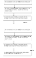
- FIG. 3 shows method steps according to an embodiment.
- critical timing parameters in the design are determined. This can be carried out in various ways.
- step 210 there is a step of selecting which of the generic logic components are in the critical timing paths.
- step 220 the fine grain tuning circuitry is added automatically to the selected generic logic components. Each of these steps can be implemented in various ways. Other steps can be added.
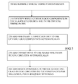
- Figure 4 shows a similar embodiment, in this case there is a further step 230 of adding connections automatically to the added fine grain circuitry.
- Figure 5 shows a similar embodiment, in this case there is a further step 240 of adding design constraints for the added fine grain tuning circuitry to the existing constraints for the design, for subsequent synthesis.
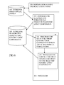
- FIG. 6 shows a schematic view of a system according to an embodiment.
- a program 300 is provided for finding critical timing paths in a stored representation 310 of a behavioural design for an integrated circuit.
- a program 320 is provided tor elaborating the behavioural design into an elaborated design 330 having generic logic components, stored for use by other programs.
- a program 340 is provided for selecting those generic components in the elaborated design which are in the critical timing paths.
- a program 350 is provided for adding automatically the fine grain tuning circuitry to the selected generic logic components.
- the various programs can be integrated together as desired. At least programs 340 and 350 are run by a processor 360. Subsequent processing steps can be carried out by this processor or by others.
- FIG. 7 shows a view of an elaborated design with the added fine grain circuitry.
- the generic logic components 520 are shown without providing detail.
- Tuning circuitry 500 is added to monitor or tune selected ones of the generic logic components.
- Additional circuitry 510 is provided for interconnection between the parts of the fine grain circuitry. Such interconnection can be in the form of scan circuitry following similar principles to the scan circuitry used conventionally for chip testing during manufacture. This can enable control or monitoring signals relating to the fine grain circuitry to be multiplexed and if needed interfaces to other parts on or off chip.
- a TAD controller 530 is provided and an IEEE 1149.1 TAP 540, to pass signals off the edge 560 of the chip to a TAD port 550.
- the elaborated design can have any kind of generic logic components, provided the interconnections equivalent to wiring interconnections are represented explicitly, so that the insertion points can be identified without needing to infer them from functional software-like features such as repeating loops.
- Blade is an example of an evolutionary RTL2RTL process that automatically inserts SKM circuits, provides flexible routing topologies, automatically connects SKM circuits, and sets their synthesis constraints. Notably this is done before synthesis.
- the Blade concept is illustrated for both a knob and a monitor circuit. More details are given on the implementation of a digital timing monitor.
- Running Blade can be as simple as sourcing one TCL script right after design elaboration. After running Blade, in the example shown in figure 7 , a set of three circuits are inserted and are connected in a proper fashion: (1) a TAD controller, (2) an IEEE 1149.1 interface controller and (3) a set of fine-grained SKM digital circuits.
- monitor and/or knob circuits This provides one example of an implementation of monitor and/or knob circuits, a controller, and a connectivity architecture. Other examples can be envisaged. Both the IEEE interface controller and the TAD controller can have the same top level architecture and named controllers.
- the TAD controller is mainly used to provide data management of the fine-grained circuits.
- the TAD controller allows control via system-level middleware software models by means of memory mapped I/O.
- the IEEE 1149.1 controller provides standard off-chip interface for runtime debugging.
- the fine-grained circuits can be a mix of SKMs. Based on the input knob or monitor architecture the Blade steps shall be tuned. Although a "Digital Delay Monitor” will be described in more detail, other examples of tuning circuitry can be envisaged or added as well. Other extensions may include ⁇ not limited to- the "Jitter Monitor", "Clock Stealing Knob” or any standard knob or monitor with a valid description preferably not synthesized in HDL.
- One major advantage of these techniques is it enables synthesizing the SKM circuits with the SoC design at the same time, which makes for a more efficient overall design procedure.
- the RTL netlist is an example of an elaborated design of generic logic components. It is effectively meta data, more like a structural VHDL design, that exhibits the same properties of RTL yet at a lower and more detailed generic abstraction level.
- the circuit components of an RTL netlist are absolutely technology independent.
- the RTL netlist is perceived by the digital design tools to be a netlist.
- the RTL netlist therefore, includes the properties of a netlist and the properties of an RTL. Blade utilizes the RTL netlist as an input.
- the Blade method utilizes a set of TCL scripts that perform automatically various operations of the method.
- the Blade TCL scripts use some extra inputs, mainly the modified SKM circuits.
- the SKM circuits must be encapsulated in a host Scan cell called in general A-Cell, MA-Cell for monitors and KA-Cell for knobs.
- the Blade methodology can incorporate five distinctive steps running at RTL level as follows:
- a standard generic scan cell architecture i.e. the A-Cell will be used, though others are possible.
- the A-Cell is the basic standard unit of the Blade performance.
- the MA-Cell is a monitor incubator cell where the monitor is described preferably at RTL level.
- the monitor output is fed internally to a data routing architecture, usually a multiplexer with a memory component i.e. DFF.
- the MA-Cell is used to (1) "Capture” runtime technology feature metrics by means of standard monitors ex. NBTI or delay timing monitors. (2) "Scan" data from previous A-Cells via the dedicated scan-in scan-out architecture.
- a generic MA-Cell as shown in Figure 9 for input requires (1) the original system clock and reset, (2) data input to be processed and monitored, (3) data input from a previous or another stage tad_si, () and a mode select input(s).
- the output is simply a scan out data pin.
- the MA-Cell includes mainly monitor description and communication architecture.
- the monitor description "MD" 420 in figure 9 could be either RTL description in HDL or a black box interface.
- the communication architecture used here is standard scan-chain architecture.
- This and the memory element 430 i.e. DFF are the main & only components of the scan-chain. Both are represented at RTL level in HDL.
- the MA-Cell architecture provided here supports continuous capture and scan. Therefore, it is subject to architectural enhancements based on the required Scan-Capture scenario. Further enhancements include (1) Shut down for minimal power usage. It is done via the extra mode_sel input. (2) Usage of more sophisticated interconnects architectures, for instance an A-Cells NOC.
- the KA-Cell is a knob incubator cell, where the knob is described preferably at RTL level. The output of the knob is fed to an external port.
- the KA-Cell is used at (1) "Force” cycle to force tuning output through the knob. (2) "Scan” data from previous A-Cells via the dedicated scan-in scan-out architecture.
- Figure 10 shows basic internal architecture.
- the generic KA-Cell shown in Figure 10 includes mainly a knob description and a communication architecture.
- the knob description "KD" 440 in the figure could be either RTL or a black box interface.
- the communication architecture used here is standard scan-chain architecture.
- the DEMUX 450 and the memory element 460 i.e. DFF are the main & only components of the scan-chain. Both are represented at RTL level.
- the DEMUX is used to route the serial input internally either to the knob i.e. KD block or to the memory element for the subsequent A-Cell.
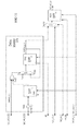
- Figure 11 Blade Example using Timing monitor in a standard MA-Cell
- Step 1 Preliminary work and Identification
- the steps include MA-Cell design, setting up the requested input files in HDL/TCL, preliminary flow runs or other.
- the digital timing delay monitor functionality is as described in above-mentioned ref 1. Briefly stated two inputs being monitored are fed to the delay monitor 670. A first of the inputs is fed to exclusive OR gate 740. A second is fed to the same gate via a delay 760 and a DFF 750. The output of the gate is fed to the select input of a multiplexer 730. This has one input tied to logic 1 and the other has a feedback signal from the output of DFF 720, which latches the output of the multiplexer 730. The output of the delay monitor 670 is fed to a multiplexer 410 and DFF 430, for the scan circuitry as explained with reference to figure 9 . Mapping the monitor architecture to the MA-Cell will result in the architecture illustrated in Figure 11 . It is evident that the design shown could be easily described at RTL level in any appropriate HDL language. Notice the gating input of the DFFs.
- Blade set-up script starts running it starts a similar sequence to this: (1) Library set-up: concatenating standard synthetic synthesis libraries to main design libraries, then concatenating the new SKM source directories to the compiler's search path. (2)TAD file system setup: Creating directories, file system and redirecting output files to proper directories. (3)Read files: reading and elaborating SKM circuits.
- Selection is the procedure of gathering the identified elements in Step 1 in an array of elements. Usually this array of elements is called a "collection" in TCL.
- the selection method is therefore supported by the programming language and could be done with 1 line of code. For example, in Code 2, a collection of all the flip-flops in a sample design excluding a specific set of flip flops i.e. FF1, FF2... etc. Similar more complex collections can be made for other components with the help of TCL scripts.
- Insertion is the procedure of creating and introducing multiple fine grained SKM circuits to design. Moreover proper connection of these SKM circuits to selected items in Step 2 is performed.
- Code 3 shows creating an MA-Cell and connecting one of its input pins to the input of a standard register i.e. creating ma_cell instances of the design ma_cell_beh, and connecting monitor_input1 to register input Q.
- Routing is the procedure of connecting multiple SKM circuits to each other.
- the communication architecture for data routing adopted in this example is the scan-chain architecture.
- Figure 7 shows the connectivity between subsequent A-Cells where output pin 'tad_so' of the first A-Cell is connected to 'tad_si' of the next A-Cell and so on.
- design constraints must be set for them separately.
- the design constraints are set iteratively for all the introduced circuits and input output connections.
- the constraints are appended to the original SoC constraints.
- these constraints are kept always in a separate script file in order to manage speedy update or a handy integration within the overall system constraints section.
- a structured RTL VHDL code is generated that is equivalent to the input SoC design.
- the only change in such a case is the increase in interface ports due to the addition of new 5 input/output pins to the SoC.
- the change is carried either via a VHDL2VHDL automated script or manually. This results in direct use of the same testbenches to double check functionality before/after adding the monitor circuits at RTL. Since the SoC is elaborated already, to simulate at such a level of detail, more GTECH libraries need to be compiled iteratively in order to conduct a successful test case exercise. To monitor the behaviour of over one hundred MA-Cells with monitor circuits during simulation of run-time, a simulation test bench script is appended to debug the whole scan chain input/output. After synthesis, similar tests are compiled.
- A-cell Monitor White box interface cell
- Standard Monitors/Knobs can have two/four modes or even more.. (update,read, write, shutdown,..). i.e. using the "tad_ms_i" and "tad_en_i" of A-Cells.
- Some examples can use fine grained standard knobs and monitors standardized insertion to overcome variability and reliability challenges in deep submicron technologies.
- An example using a crystal ball timing monitor has been described.
- the method and circuits can be used in a 65nm ASIC chip.
- the method has proved the concept for standardized monitors and can be easily extended to include different tuning circuitry.
- This approach enables runtime gathering information concerning the impact of aging and/or process variation at the very fine grain level of generic logic circuits. This information is useful to calibrate higher design abstraction level models at system level. Having control from a middle ware on such fine grained SKM structures, enable chips to consume less power, live longer and eventually behave as intended statistically.
Landscapes
- Engineering & Computer Science (AREA)
- Computer Hardware Design (AREA)
- Physics & Mathematics (AREA)
- Theoretical Computer Science (AREA)
- Evolutionary Computation (AREA)
- Geometry (AREA)
- General Engineering & Computer Science (AREA)
- General Physics & Mathematics (AREA)
- Design And Manufacture Of Integrated Circuits (AREA)
Priority Applications (2)
| Application Number | Priority Date | Filing Date | Title |
|---|---|---|---|
| EP11154244A EP2487614A1 (fr) | 2011-02-11 | 2011-02-11 | Ajout de circuit de réglage de grain fin à un design de circuit intégré |
| US13/370,167 US20120210286A1 (en) | 2011-02-11 | 2012-02-09 | Adding fine grain tuning circuitry to integrated circuit design |
Applications Claiming Priority (1)
| Application Number | Priority Date | Filing Date | Title |
|---|---|---|---|
| EP11154244A EP2487614A1 (fr) | 2011-02-11 | 2011-02-11 | Ajout de circuit de réglage de grain fin à un design de circuit intégré |
Publications (1)
| Publication Number | Publication Date |
|---|---|
| EP2487614A1 true EP2487614A1 (fr) | 2012-08-15 |
Family
ID=43769269
Family Applications (1)
| Application Number | Title | Priority Date | Filing Date |
|---|---|---|---|
| EP11154244A Withdrawn EP2487614A1 (fr) | 2011-02-11 | 2011-02-11 | Ajout de circuit de réglage de grain fin à un design de circuit intégré |
Country Status (2)
| Country | Link |
|---|---|
| US (1) | US20120210286A1 (fr) |
| EP (1) | EP2487614A1 (fr) |
Cited By (1)
| Publication number | Priority date | Publication date | Assignee | Title |
|---|---|---|---|---|
| CN117764020A (zh) * | 2024-02-22 | 2024-03-26 | 沐曦集成电路(上海)有限公司 | 芯片设计调整方法、电子设备和介质 |
Families Citing this family (6)
| Publication number | Priority date | Publication date | Assignee | Title |
|---|---|---|---|---|
| US8601412B1 (en) * | 2011-11-18 | 2013-12-03 | Cadence Design Systems, Inc. | Netlisting analog/mixed-signal schematics to VAMS |
| US11270053B2 (en) * | 2016-07-08 | 2022-03-08 | efabless corporation | Systems and methods for assembling and developing an SoC efficiently using templates and designer input data |
| EP3361637A1 (fr) * | 2017-02-09 | 2018-08-15 | Nxp B.V. | Procédé et circuit numérique synchrone pour empêcher la propagation d'erreurs de données de synchronisation d'installation |
| US12175176B2 (en) * | 2021-03-17 | 2024-12-24 | Synopsys, Inc. | Fast synthesis of logical circuit design with predictive timing |
| US11803684B1 (en) * | 2021-10-04 | 2023-10-31 | Cadence Design Systems, Inc. | Relative placement by application of layered abstractions |
| US12406119B2 (en) * | 2021-12-03 | 2025-09-02 | International Business Machines Corporation | Processor chip timing adjustment enhancement |
Family Cites Families (5)
| Publication number | Priority date | Publication date | Assignee | Title |
|---|---|---|---|---|
| US6130551A (en) * | 1998-01-19 | 2000-10-10 | Vantis Corporation | Synthesis-friendly FPGA architecture with variable length and variable timing interconnect |
| US7240302B1 (en) * | 2004-12-23 | 2007-07-03 | Altera Corporation | Method and apparatus for relocating elements in a floorplan editor |
| US7743354B2 (en) * | 2007-05-02 | 2010-06-22 | Cadence Design Systems, Inc. | Optimizing integrated circuit design through use of sequential timing information |
| US7739642B2 (en) * | 2007-05-02 | 2010-06-15 | Cadence Design Systems, Inc. | Optimizing integrated circuit design through balanced combinational slack plus sequential slack |
| US7669161B2 (en) * | 2007-06-22 | 2010-02-23 | Synopsys, Inc. | Minimizing effects of interconnect variations in integrated circuit designs |
-
2011
- 2011-02-11 EP EP11154244A patent/EP2487614A1/fr not_active Withdrawn
-
2012
- 2012-02-09 US US13/370,167 patent/US20120210286A1/en not_active Abandoned
Non-Patent Citations (3)
| Title |
|---|
| ABDELHAMID A ET AL: "A Standardized Knobs and Monitors RTL2RTL Insertion Methodology for Fine Grain SoC Tuning", DIGITAL SYSTEM DESIGN, ARCHITECTURES, METHODS AND TOOLS, 2009. DSD '09. 12TH EUROMICRO CONFERENCE ON, IEEE, PISCATAWAY, NJ, USA, 27 August 2009 (2009-08-27), pages 401 - 408, XP031578181, ISBN: 978-0-7695-3782-5 * |
| ABDELHAMID, A.; ANCHLIA, A.; MAMAGKAKIS, S.; MIRANDA, M.C.; DIERICKX, B.; KUIJK, M.: "A Standardized Knobs and Monitors RTL2RTL Insertion Methodology for Fine Grain SoC Tuning", DIGITAL SYSTEM DESIGN, ARCHITECTURES, METHODS AND TOOLS, 2009. DSD '09. 12TH EUROMICRO CONFERENCE ON, 27 August 2009 (2009-08-27), pages 401 - 408 |
| NAESSENS, F.; DERUDDER, V.; CAPPELLE, H.; HOLLEVOET, L.; RAGHAVAN, P.; DESMET, M.; ABDELHAMID, A.; VOS, I.; FOLENS, L.; O'LOUGHLIN: "A 10.37 mm2 675 mW reconfigurable LDPC and Turbo encoder and decoder for 802.11n, 802.16e and 3GPP-LTE", VLSI CIRCUITS (VLSIC), 2010 IEEE SYMPOSIUM ON, 16 June 2010 (2010-06-16), pages 213 - 214 |
Cited By (2)
| Publication number | Priority date | Publication date | Assignee | Title |
|---|---|---|---|---|
| CN117764020A (zh) * | 2024-02-22 | 2024-03-26 | 沐曦集成电路(上海)有限公司 | 芯片设计调整方法、电子设备和介质 |
| CN117764020B (zh) * | 2024-02-22 | 2024-04-26 | 沐曦集成电路(上海)有限公司 | 芯片设计调整方法、电子设备和介质 |
Also Published As
| Publication number | Publication date |
|---|---|
| US20120210286A1 (en) | 2012-08-16 |
Similar Documents
| Publication | Publication Date | Title |
|---|---|---|
| US8875071B2 (en) | Deployment of custom shift array macro cells in automated application specific integrated circuit design flow | |
| US8775985B2 (en) | Computer-aided design system to automate scan synthesis at register-transfer level | |
| US7340700B2 (en) | Method for abstraction of manufacturing test access and control ports to support automated RTL manufacturing test insertion flow for reusable modules | |
| Chang et al. | Automating post-silicon debugging and repair | |
| EP2487614A1 (fr) | Ajout de circuit de réglage de grain fin à un design de circuit intégré | |
| US7055118B1 (en) | Scan chain verification using symbolic simulation | |
| US7693676B1 (en) | Low power scan test for integrated circuits | |
| Kuppuswamy et al. | Full Hold-Scan Systems in Microprocessors: Cost/Benefit Analysis. | |
| US8789004B2 (en) | Automatic flow of megacell generation | |
| CN102831272B (zh) | 用于双边沿触发器的可测试性设计方法 | |
| JP2004342100A (ja) | 集積回路の物理設計用のツールフロープロセス | |
| US9449127B1 (en) | System for verifying timing constraints of IC design | |
| US12007440B1 (en) | Systems and methods for scan chain stitching | |
| Han et al. | Embedded test decompressor to reduce the required channels and vector memory of tester for complex processor circuit | |
| US8943457B2 (en) | Simulating scan tests with reduced resources | |
| Doerre et al. | The IBM ASIC/SoC methodology—A recipe for first-time success | |
| JP2010257003A (ja) | 論理等価性検証システム、論理等価性検証方法、半導体集積回路の製造方法、制御プログラムおよび可読記憶媒体 | |
| Engel et al. | Design methodology for IBM ASIC products | |
| Golshan | ASIC Design Implementation Process | |
| Shi et al. | Testing delay faults in asynchronous handshake circuits | |
| Ravikumar et al. | A holistic parallel and hierarchical approach towards design-for-test | |
| Ranerup et al. | Using formal verification to exhaustively verify SoC assemblies | |
| Indino | An open source platform and EDA tool framework to enable scan test power analysis testing | |
| CN121706689A (zh) | 一种用于可测试性设计的片上时钟控制器及其优化方法 | |
| Hemal et al. | Modified Boundary Scan Cell for Faster Continuous Monitoring |
Legal Events
| Date | Code | Title | Description |
|---|---|---|---|
| PUAI | Public reference made under article 153(3) epc to a published international application that has entered the european phase |
Free format text: ORIGINAL CODE: 0009012 |
|
| 17P | Request for examination filed |
Effective date: 20110808 |
|
| AK | Designated contracting states |
Kind code of ref document: A1 Designated state(s): AL AT BE BG CH CY CZ DE DK EE ES FI FR GB GR HR HU IE IS IT LI LT LU LV MC MK MT NL NO PL PT RO RS SE SI SK SM TR |
|
| AX | Request for extension of the european patent |
Extension state: BA ME |
|
| 17Q | First examination report despatched |
Effective date: 20120823 |
|
| STAA | Information on the status of an ep patent application or granted ep patent |
Free format text: STATUS: THE APPLICATION IS DEEMED TO BE WITHDRAWN |
|
| 18D | Application deemed to be withdrawn |
Effective date: 20160901 |