EP3361637A1 - Procédé et circuit numérique synchrone pour empêcher la propagation d'erreurs de données de synchronisation d'installation - Google Patents
Procédé et circuit numérique synchrone pour empêcher la propagation d'erreurs de données de synchronisation d'installation Download PDFInfo
- Publication number
- EP3361637A1 EP3361637A1 EP17155429.8A EP17155429A EP3361637A1 EP 3361637 A1 EP3361637 A1 EP 3361637A1 EP 17155429 A EP17155429 A EP 17155429A EP 3361637 A1 EP3361637 A1 EP 3361637A1
- Authority
- EP
- European Patent Office
- Prior art keywords
- clock
- data
- timing
- timing error
- digital circuit
- Prior art date
- Legal status (The legal status is an assumption and is not a legal conclusion. Google has not performed a legal analysis and makes no representation as to the accuracy of the status listed.)
- Withdrawn
Links
Images



Classifications
-
- H—ELECTRICITY
- H03—ELECTRONIC CIRCUITRY
- H03K—PULSE TECHNIQUE
- H03K5/00—Manipulating of pulses not covered by one of the other main groups of this subclass
- H03K5/19—Monitoring patterns of pulse trains
-
- G—PHYSICS
- G06—COMPUTING OR CALCULATING; COUNTING
- G06F—ELECTRIC DIGITAL DATA PROCESSING
- G06F30/00—Computer-aided design [CAD]
- G06F30/30—Circuit design
- G06F30/32—Circuit design at the digital level
- G06F30/33—Design verification, e.g. functional simulation or model checking
- G06F30/3308—Design verification, e.g. functional simulation or model checking using simulation
- G06F30/3312—Timing analysis
-
- G—PHYSICS
- G06—COMPUTING OR CALCULATING; COUNTING
- G06F—ELECTRIC DIGITAL DATA PROCESSING
- G06F1/00—Details not covered by groups G06F3/00 - G06F13/00 and G06F21/00
- G06F1/04—Generating or distributing clock signals or signals derived directly therefrom
- G06F1/12—Synchronisation of different clock signals provided by a plurality of clock generators
-
- G—PHYSICS
- G01—MEASURING; TESTING
- G01R—MEASURING ELECTRIC VARIABLES; MEASURING MAGNETIC VARIABLES
- G01R31/00—Arrangements for testing electric properties; Arrangements for locating electric faults; Arrangements for electrical testing characterised by what is being tested not provided for elsewhere
- G01R31/28—Testing of electronic circuits, e.g. by signal tracer
- G01R31/317—Testing of digital circuits
- G01R31/31725—Timing aspects, e.g. clock distribution, skew, propagation delay
- G01R31/31726—Synchronization, e.g. of test, clock or strobe signals; Signals in different clock domains; Generation of Vernier signals; Comparison and adjustment of the signals
-
- G—PHYSICS
- G06—COMPUTING OR CALCULATING; COUNTING
- G06F—ELECTRIC DIGITAL DATA PROCESSING
- G06F11/00—Error detection; Error correction; Monitoring
- G06F11/07—Responding to the occurrence of a fault, e.g. fault tolerance
- G06F11/16—Error detection or correction of the data by redundancy in hardware
- G06F11/1604—Error detection or correction of the data by redundancy in hardware where the fault affects the clock signals of a processing unit and the redundancy is at or within the level of clock signal generation hardware
-
- G—PHYSICS
- G06—COMPUTING OR CALCULATING; COUNTING
- G06F—ELECTRIC DIGITAL DATA PROCESSING
- G06F30/00—Computer-aided design [CAD]
- G06F30/30—Circuit design
- G06F30/35—Delay-insensitive circuit design, e.g. asynchronous or self-timed
-
- H—ELECTRICITY
- H03—ELECTRONIC CIRCUITRY
- H03K—PULSE TECHNIQUE
- H03K19/00—Logic circuits, i.e. having at least two inputs acting on one output; Inverting circuits
- H03K19/003—Modifications for increasing the reliability for protection
- H03K19/00369—Modifications for compensating variations of temperature, supply voltage or other physical parameters
- H03K19/00384—Modifications for compensating variations of temperature, supply voltage or other physical parameters in field effect transistor circuits
-
- H—ELECTRICITY
- H03—ELECTRONIC CIRCUITRY
- H03K—PULSE TECHNIQUE
- H03K5/00—Manipulating of pulses not covered by one of the other main groups of this subclass
- H03K5/22—Circuits having more than one input and one output for comparing pulses or pulse trains with each other according to input signal characteristics, e.g. slope, integral
-
- H—ELECTRICITY
- H04—ELECTRIC COMMUNICATION TECHNIQUE
- H04L—TRANSMISSION OF DIGITAL INFORMATION, e.g. TELEGRAPHIC COMMUNICATION
- H04L7/00—Arrangements for synchronising receiver with transmitter
- H04L7/0054—Detection of the synchronisation error by features other than the received signal transition
Definitions
- This disclosure relates to synchronous digital circuits, and to methods of avoiding set-up timing data errors in data propagating from logic to a hard macro, in such a synchronous digital circuit.
- Synchronous digital circuits can be subject to set-up timing errors.
- a set-up timing error occurs when the circuit does not achieve a specific well-defined data state - either high or low - before the subsequent rising edge of the clock signal.
- Setup timing errors can occur due to several reasons, such as ageing, voltage scaling, frequency scaling, etc.
- Set-up timing errors can be detected using, for example, double sampling flip-flops. Once an error is detected, it can generally be masked, for instance by "borrowing" time from a subsequent stage, in particular the next downstream pipeline stage, which is typically a further logic block. The error, thus masked, propagates through the logic without causing failures. However, in some architectures, this may not be possible, in particular in the presence of a hard macro. As will be described in more detail hereinbelow, in this disclosure, a hard macro, also known as hard core of hard IP, refers to a circuit element or block, at the input of which timing errors either cannot be tolerated, or are undetectable.
- a synchronous digital circuit having a system clock and for processing a data signal
- the digital circuit comprises: a data path; a hard macro having a macro input; a logic circuit in the data path upstream of the macro input and having a first part and a second part, the second part being immediately upstream of the macro input; a set-up timing error detector having an input, wherein the input is on the data path between the first part and the second part; and a timing correction unit: wherein - during normal operation - the data transit time across the second part is equal to or less than one half of a clock period, and wherein the timing correction unit is configured to correct, in response to the set-up timing error detector detecting a set-up timing error, the detected set-up timing error before the data reaches the macro input.
- the set-up timing error detector is in the data path and between the first part of the logic circuit and the second part of the logic circuit. In one or more other embodiments, the set-up timing detector is not in the data path, and in the data path the first part of the logic circuit is adjacent the second part of the logic circuit in the data path. Including the set-up timing error detector in the data path may be beneficial, since the overall flow is simplified; conversely, having the set-up timing error detector not in the data path may, for one or more embodiments, save some time: since letting the data traverse through the detector also involves passing it through some cells; this has the effect of slowing the data down. This doesn't happen when the data doesn't pass through the detector but instead the detector only samples the data and flags an error if needed.
- the timing error detector comprises a flag, configured to flag an error to the timing correction unit.
- the timing error detector comprises a double sampling flip-flop having a clock input which is an inverted system clock.
- a similar circuit design is used instead of a DSFF, for instance a logical combination of latches may be used to achieve the same or similar result - in particular to detect and flag a later-than-expected data transition.
- the double sampling flip-flop further comprises a delayed clock input which is a delayed inverted system clock.
- the timing correction unit comprises a clock gating unit configured to gate the clock in response to detection of a set-up timing error. In one or more other embodiments, the timing correction unit comprises a clock stretcher configured to stretch the clock in response to detection of a set-up timing error. In such embodiments or other embodiments, the timing correction unit may form part of a clock generation unit for providing the system clock. In yet other embodiments, the timing correction unit comprises one of (a) a voltage adjustment unit configured to adjust a voltage of the synchronous digital circuit, so as to speed up the clock, and (b) a body biasing adjustment circuit configured to adapt the bias of the body of the synchronous digital circuit, in response to detection of a set-up timing error.
- the hard macro is an SRAM. In other embodiments, the hard macro is a Graphics Processing Unit (GPU). Typically, but without limitation, the hard macro may be precompiled and such that the circuit designer cannot edit or synthesize it. In general, a hard macro, which may also be referred to as a hard core, is such that if an error propagates into it, the error is undetectable and unrecoverable. As used herein, a "hard" macro may be distinguished from a "soft macro”: in the case of a soft macro, it is possible to detect and correct an error, which has propagated into the macro. According to another aspect of the present disclosure there is provided an electronic component comprising a synchronous digital circuit as described above. The electronic component may be, for example, one of a microcontroller, a digital signal processor and a graphics processing unit.
- the electronic component may be, for example, one of a microcontroller, a digital signal processor and a graphics processing unit.
- a method a preventing set-up timing data errors in data propagating from logic to a hard macro, the logic and hard macro both comprised in a synchronous digital circuit comprising: detecting a set-up timing error, by means of a set-up timing error detector, within one half of a normal operation clock period prior to the data reaching the hard macro, and correcting, in response to detecting a set-up timing error, the detected set-up timing error before the data reaches the macro input.
- detecting a set-up timing error comprises double sampling the data by a double sampling flip-flop.
- correcting the detected set-up timing error comprises gating a system clock or stretching the system clock, and replacing the data by the second sample of the double sampling flip-flop. In one or more other embodiments, correcting the detected set-up timing error comprises adjusting an operating voltage of the synchronous digital circuit, and replacing the data by the second sample of the double sampling flip-flop: since the data has less time to travel through the second part of the logic, compensation is needed. This may be done by increasing the logic voltage (Vdd): that is to say, when an error is detected, the Vdd of the core logic should be increased, which allows the data to move faster through the logic. The clock period itself is not affected. Alternatively and without limitation, a biasing voltage may be applied to the bulk of the transistors in the logic cells, that is to say, 'forward body biasing' is used - which will also increase the speed of the data traveling through the logic.
- Vdd logic voltage
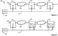
- Figure 1 shows a typical path in a synchronous digital design 100, having logic blocks 110 and 120, and including regular flip-flops 130, 140, and 150.
- the path includes a data signal 160 and a clock signal 170.
- the clock signal 170 is a system clock generated by a clock generation unit (CGU) 180, and supplied as the clock input CLK to each of the flip-flops.
- the system clock may be a local clock or may be a universal clock.
- the data output from each logic stage also referred to as a pipeline stage, is input to the subsequent flip-flop at data input D, and the flip-flop latched output Q is supplied as input to the next logic stage.
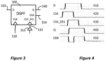
- FIG. 2 shows the same path 100 wherein the flip-flops 140 and 150 are replaced by double sampling flip-flops (DSFF) 240 and 250.
- DSFFs allow set-up timing errors to be detected, as will be described with reference to figures 3 and 4 .
- Figure 3 shows the pins of a DSFF.
- the data input D 310 it has two clock inputs: the first is the normal clock input CLK 320, and the other is a delayed clock CLK_DEL 330.
- the delay is introduced by adding a buffer 355 in the clock line to the delayed clock input CLK-DEL. Note that this is one solution to generate the delayed clock but others are possible.
- the DSFF has a second output ERR 350. Use of DSFFs instead of regular flip-flops allows the detection of set-up timing errors, and provides a flag on output ERR, when a set-up timing error is detected.
- FIG. 4 shows a data signal at 410, clock signal CLK at 420, delayed clock CLK_DEL at 430, Latch Q at 440 and error flag ERR at 450.
- the data D has not settled prior to the rising edge of the clock signal CLK. Instead, the data D changes half way between the rising edge of CLK and CLK_DEL.
- the flip-flop is able to register the new data on the latch output Q and also flags the ERR signal between the rising edge of CLK_DEL and the falling edge of CLK.
- the error signal is an active low error signal.
- the duration of the delay between the clock signal CLK and the delayed clock CLK_DEL defines the width of the checking window. In an extreme case, in which the data change is delayed by more than the offset between CLK and CLK_DEL, the timing error would not be detected. It will be appreciated that the size or width of the checking window may be adjusted. Adjustment is done by increasing the delay between the clock and the delayed clock. The size or width of the checking window determines the amount of variability in the data signal which the system can deal with.
- Masking an error may include letting the error propagate to a next stage of the logic, which next stage has sufficient slack to absorb the error. Correcting an error may be done for instance, by clock stretching, as illustrated in Figure 5 .
- Figure 5 shows a data signal Data, 510, a clock signal CLK 520, a delayed clock CLK-DEL 530 and an active low error flag ERR 540. Note that in this figure, both high and low states of the data signal are shown: the crossover points mark moments of possible changes in the signal - irrespective of whether a transition actually occurs; it will be appreciated that a the "high-high” and "low-low” non-transitions are omitted for clarity.
- the delayed clock is delayed by one quarter of a clock period.
- the checking window 550 is thus equal to one quarter of a clock period.
- the checking window between the rising edge of CLK and CLK_DEL may be defined by including a buffer between the CLK and CLK_DEL, as shown in figure 3 , or otherwise.
- the first data transition 512 does not have any timing error, that is to say it occurs ahead of the rising edge 522 of CLK 520.
- the subsequent data transition is subject to a timing error such that it occurs after the rising edge 524 of CLK 520.
- the first sampling of the flip-flop does not register the data transition.
- the data transition 514 occurs ahead of, and is stable by the time of, the second, delayed, clock CLK_DEL. So the second sampling, which is triggered by the delayed clock, does register the transition, and the "correct" output may be latched (not shown).
- the difference between the outputs from the first sampling and the second sampling triggers the ERR flag 540 to go active (i.e. low in this example).
- error flag ERR is asserted only until the falling edge of the system clock, at which time it is reset. It will be recognised that in other examples the error flag may be latched until corrective action is completed.
- clock stretching involves delaying a rising edge of the clock signal CLK, by a stretching interval S (shown at 560 in figure 5 ). Ideally, the stretching interval 560 is the same duration as the checking window. Since the CLK has been stretched by a duration which is at least as great as the timing-error offset then, absent another set-up timing error during this clock period, the logic in the next cell should have time to settle prior to the subsequent rising edge of the clock.
- a scheme such as clock gating may be used in which the clock is stopped for one complete cycle in order to give the data more time to arrive at the next flip-flop.
- the error may be self-correcting, for instance where the next pipeline stage is relatively short, so the logic has time to settle in less than one complete clock period but within the shortened clock period between the rising edge of CLK_DEL and the subsequent rising edge of CLK.
- a hard macro such as an SRAM, or other hard core.
- An example such data path is shown in figure 6 , which is similar to that shown in figure 2 , except that the DSFF flip-flop 250 is replaced by a hard macro - in this case an SRAM 650.
- a macro, and more specifically a hard macro may be considered as a 'black-box' which is not accessible and hence no extra double sampling flip-flops or other methods can be integrated in them.
- An example of a hard macro is memory, such as the SRAM shown in figure 6 .
- a hard macro e.g. a memory
- All timing errors must be both detected fixed before the data reaches the hard macro, that is to say, in the case of a memory, the correct signals have to go into the memory to ensure correct operation.
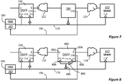
- the arrangement comprises a set-up timing error detector 790, positioned in the data path close to the macro. Specifically, as will be discussed in more detail below, the detector should be within one half clock period of the macro - to ensure that no setup timing errors are generated between the detector and the hard macro. It will be appreciated that a reference such "no more than one half clock period" refers to the time it takes for data to transit the respective logic block. If the logic block immediately upstream of the hard macro is more than half a clock period in duration, the logic block should be split, as shown, into two parts 122 and 124, with the detector 790 therebetween. The logic block second part 124 between the detector 790 and the hard macro is no more than one half clock period.
- a setup timing error when detected by the detector, it has to be corrected before it reaches the macro.
- the error correction may be done by means of clock gating or by using a clock stretcher which provides a fast, and less throughput-constraining, method of error correction.
- the arrangement includes a feedback path 795 from the detector to a timing correction unit 780, which may use clock gating, clock stretching or other functionality to correct the error before it propagates to the hard macro.
- a synchronous digital circuit according to the present disclosure may provide a way to accommodate timing changes in the design due to various sources (e.g. aging, voltage scaling, frequency scaling, etc.) by detecting timing errors and correcting them before the error reaches the hard macro, and thereby ensuring the correct value is input into the hard macro.
- the detector may be closer to the macro than one half of a clock period; however, since it is required that any errors detected by the detector are also corrected by the time the signal reaches the macro, placing the detector closer to the macro imposes a tighter constraint on the operation of the timing correction unit. Moreover, since there needs to be a match between the data D which is latched and the clock, if the detector is placed closer to the macro than one half clock period, it may be more complicated to match the clock with the expected data value at that clock, as will be discussed further hereinbelow.
- the timing correction unit 780 may be part of the clock generation unit 180 to facilitate clock getting or clock stretching.
- the timing correction unit utilises dynamic voltage scaling (not shown).
- the error signal can be fed to the power management unit of the system, where it provides an indication that the system or sub-system voltage needs to be increased to make the system faster.
- the circuit may be used to determine a lowest safe operating voltage maintaining the same throughput: for example, the system may be run, and the voltage decreased stepwise until the detector starts to flag errors, which are corrected by the timing correction unit, thereby reducing the throughput. The operating voltage may then be increased, until no errors are flagged - consequently the throughput reverts to the original throughput. The voltage then is the lowest voltage at which the system can be run with the same throughput as for the nominal voltage. Power will be saved provided this lowest safe running voltage is lower than the nominal voltage.
- the set-up timing detector 790 takes the form of a DSFF. This is shown in figure 8 , in which a DSFF 890 is positioned in the data path, no more than one half-cycle upstream of the hard macro.
- the DSFF has a data input 892 from the upstream logic block first part 122, and a latched output Q 894 which acts as input to the downstream logic block second part 124 which is immediately upstream of the hard macro.
- the DSFF has a clock input 896 and a delayed clock input 898. The delay may be implemented by the inclusion of a buffer 895 between the clock and the delayed clock.
- the DSFF clock is exactly one half period behind the main i.e. system clock generated by the CGU 180. That is to say, the DSFF clock is an inverted copy of the system clock. This is illustrated in figure 8 by the inverter 885.
- the DSFF delayed clock CLK_DEL is offset from an inverted system clock by an equivalent off-set delta_t. This may be done, for example, by increasing the buffer time of buffer 895, effectively increasing the checking window. However, the chances are then higher that the CLK_INV latches incorrect data.
- An alternative solution (not shown in figure 8 ) is to add a buffer before (or after) the inverter 885, effectively shifting the whole checking window.
- a delayed clock may be provided throughout the whole chip, resulting in two clock trees, one regular and one delayed - although this would likely result in of a lot of additional area requirement, and routing issues.
- an inverted clock may be provided throughout the whole chip.
- the system should take corrective measures.
- This may be in the form of clock gating or something more elaborate such as clock stretching, but also may be in dynamic voltage scaling or adaptive body biasing, or other such techniques, in which adjustment of the system voltage leads to a change in clock period.
- the corrective measures in this case have to be activated before the data reaches the hard macro which is within half a clock period of the detector. That is to say, it is necessary that the corrective action must be initiated prior to the data, which is potentially corrupted, reaching the hard macro.
- the corrective measures involve “stopping the clock", by for instance clock stretching or clock gating
- the corrective measures do not need necessarily to be completed before the end of a standard clock half-period (that is to say, half of a clock cycle of an un-altered free-running clock); however, it is required that the corrective measures are complete before the data reaches the hard macro - that is to say, within the remaining part of the clock cycle of the local clock, taking into account clock stretching or clock gating.
- Figure 9 illustrates a method according to the present disclosure.
- Figure 9 depicts a data signal Data, 910 (showing both high and low states and, diagrammatically, the moments of possible transition), a clock signal CLK 920 and delayed clock CLK_DEL 930, similar to the conventional circuit of Figure 5 .
- the delayed clock is delayed by one quarter of a clock period.
- the checking window 970 is thus equal to one quarter of a clock period.
- the checking window between the rising edge of CLK and CLK_DEL may be defined by including a buffer between the CLK and CLK_DEL, as shown in figure 3 , or otherwise.
- this figure also incorporates a set-up timing error detector in the form of a DSFF having an inverted clock CLK_INV 950, and a delayed inverted clock CLK_INV_DEL 960, and an active low error flag ERR 940.
- the first two shown data transitions 912 and 914 do not have any timing error, that is to say they occur ahead of the rising edge 922 and 924 of CLK 920.
- the timing error in the logic such that a transition 916 (which should occur before the half-cycle moment, occurs later than expected. That is to say it occurs after the falling edge 925 of CLK 920, rather than before it, and thus after the rising edge 954 of the invented clock CLK_INV 950.
- the first sampling of the set-up timing error flip-flop 890 does not register the data transition.
- the data transition 916 occurs ahead of, and is stable by the time of, the rising edge of the second, delayed clock, CLK_INV_DEL, after the checking window 975. So the second sampling, which is triggered by the delayed clock, does register the transition, and the "correct" output may be latched (not shown).
- the difference between the outputs from the first sampling and the second sampling triggers the ERR flag 940 (i.e. it goes low in this example).
- the system responds to this by applying a corrective measure, which in this example is done with the help of clock stretching.
- the clock stretcher delays the clock signal by a certain amount of time (in this case a quarter of the period), in order for the data to arrive on time.
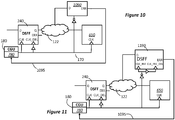
- FIG 10 Another embodiment according to the present disclosure is shown in figure 10 .
- This embodiment is similar to that shown in figure 7 , except that, in this case, the set-up timing error detector 1090 is not in the logic path. Rather, an input to the set-up timing error detector 1090 is provided from a point in the logic path which is equal to or less than one half of a clock period from the hard macro. Thus the logic does not need to be split into two separate parts: they may instead be contiguous or adjacent.
- the set-up timing error detector 1090 has an inverted clock input, and an error flag output ERR which provides an error feedback path 1095.
- the feedback path 1095 from the detector may be to a timing correction unit 780 forming part of the clock generation unit, similar to the embodiment shown in figure 7 ; alternatively and without limitation it may be fed to the power management unit of the system, where it may provide an indication that the system or sub-system voltage needs to be increased to make the system faster.
- Figure 11 shows another embodiment which is similar to that shown in figure 10 , except that the set-up timing error detector be implemented as a DSFF 1190.
- the feedback path 1095 from the detector may be to a timing correction unit 780 forming part of the clock generation unit, as shown; alternatively and without limitation it may be fed to the power management unit of the system, where it may provide an indication that the system or sub-system voltage needs to be increased to make the system faster.
- Figure 12 depicts a flow diagram of a method a preventing set-up timing data errors in data propagating from logic to a hard macro, the logic and hard macro both comprised in a synchronous digital circuit.
- 1210 shows the step of detecting a set-up timing error, by means of a set-up timing error detector, within one half of a normal operation clock period prior to the data reaching the hard macro.
- step 1220 is shown correcting, in response to detecting a set-up timing error, the detected set-up timing error before the data reaches the macro input.
- FIG. 1310 shows the step of detecting a set-up timing error, by means of a set-up timing error detector, within one half of a normal operation clock period prior to the data reaching the hard macro.
- Correcting, in response to detecting a set-up timing error, the detected set-up timing error before the data reaches the macro input comprises gating a system clock or stretching the system clock shown at 1320, and replacing the data by the second sample of the double sampling flip-flop, shown at 1330.
- correction of the set-up timing data error is effected by means of voltage scaling or similar techniques.
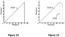
- Figures 14 and 15 illustrate the performance of a synchronous digital circuit without and with set-up timing error detection and correction respectively, shown as terms of throughput (on the y-axis or ordinate), plotted against clock speed (on the x-axis or abscissa).
- the frequency 1410 can be increased up until a point where timing requirements can no longer be met and at that point the system will fail.
- the illustrative figure shows that at frequency '7', the throughput of the system drops to zero because of incorrect latching of signals.
- FIG. 15 shows the behaviour of a system in which setup-timing error detection and correction immediately upstream of a hard macro (as per figure 14 ).
- the line 1510 shows the behaviour of a system according to embodiments of the present disclosure. Instead of failing at a frequency of '7', the frequency can be further increased. This is due to the fact that the 'macro monitoring' (i.e.
- setup-timing error detection and correction immediately upstream of a hard macro grants the system more time by taking corrective measures when data to a hard macro starts to present timing issues.
- the throughput at that point drops since the macro monitor will flag an error and thus activate the corrective measures (such as clock stretching or the like), which will lower the performance but without incurring a system failure.
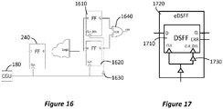
- the detector may be implemented as a double sampling flip flop, as described above. However, the disclosure is not limited thereto, and the skilled person will readily appreciate that other implementation are possible. For example, the detector may be implementation as separate flip-flops where the inputs are tied. The clock to one is the regular clock and the clock to the second one is the delayed clock. The outputs go to an exclusive OR and this can flag the error.
- FIG. 16 Such a detector is illustrated in Figure 16 , which shows two flip-flops 1610 and 1620; the clock input to the second flip-flop 1620 is delayed by the inclusion of the buffer 1630, relative to the clock input to the first flip-flop 1610.
- the data inputs D are tied.
- the outputs are combined by XOR logic 1640, the output from which is the error flag ERR.
- FIG. 17 Another example of such a detector is shown in Figure 17 .
- a double sampling flip-flop (DSFF) 1710 is fully enclosed, as part of a cell 1720 which includes not only the DSFF but also a clock delay buffer 1730 such that it is necessary to provide only one clock from the outside. It will be appreciated that for such an embodiment, it may not be possible to change the delay and therefor the checking window.
- DSFF double sampling flip-flop
Landscapes
- Engineering & Computer Science (AREA)
- Physics & Mathematics (AREA)
- Theoretical Computer Science (AREA)
- General Engineering & Computer Science (AREA)
- Computer Hardware Design (AREA)
- General Physics & Mathematics (AREA)
- Nonlinear Science (AREA)
- Evolutionary Computation (AREA)
- Geometry (AREA)
- Computing Systems (AREA)
- Mathematical Physics (AREA)
- Computer Networks & Wireless Communication (AREA)
- Signal Processing (AREA)
- Quality & Reliability (AREA)
- Manipulation Of Pulses (AREA)
- Logic Circuits (AREA)
- Synchronisation In Digital Transmission Systems (AREA)
Priority Applications (3)
| Application Number | Priority Date | Filing Date | Title |
|---|---|---|---|
| EP17155429.8A EP3361637A1 (fr) | 2017-02-09 | 2017-02-09 | Procédé et circuit numérique synchrone pour empêcher la propagation d'erreurs de données de synchronisation d'installation |
| CN201810139921.4A CN108446439A (zh) | 2017-02-09 | 2018-02-09 | 用于防止设置时序数据误差的传播的方法和同步数字电路 |
| US15/911,901 US10534396B2 (en) | 2017-02-09 | 2018-03-05 | Method, and a synchronous digital circuit, for preventing propagation of set-up timing data errors |
Applications Claiming Priority (1)
| Application Number | Priority Date | Filing Date | Title |
|---|---|---|---|
| EP17155429.8A EP3361637A1 (fr) | 2017-02-09 | 2017-02-09 | Procédé et circuit numérique synchrone pour empêcher la propagation d'erreurs de données de synchronisation d'installation |
Publications (1)
| Publication Number | Publication Date |
|---|---|
| EP3361637A1 true EP3361637A1 (fr) | 2018-08-15 |
Family
ID=58094178
Family Applications (1)
| Application Number | Title | Priority Date | Filing Date |
|---|---|---|---|
| EP17155429.8A Withdrawn EP3361637A1 (fr) | 2017-02-09 | 2017-02-09 | Procédé et circuit numérique synchrone pour empêcher la propagation d'erreurs de données de synchronisation d'installation |
Country Status (3)
| Country | Link |
|---|---|
| US (1) | US10534396B2 (fr) |
| EP (1) | EP3361637A1 (fr) |
| CN (1) | CN108446439A (fr) |
Cited By (1)
| Publication number | Priority date | Publication date | Assignee | Title |
|---|---|---|---|---|
| EP3923472A1 (fr) * | 2020-06-08 | 2021-12-15 | Nxp B.V. | Circuit de détection et de correction d'erreurs de synchronisation |
Families Citing this family (4)
| Publication number | Priority date | Publication date | Assignee | Title |
|---|---|---|---|---|
| US10365327B2 (en) | 2017-10-18 | 2019-07-30 | International Business Machines Corporation | Determination and correction of physical circuit event related errors of a hardware design |
| CN113644913B (zh) * | 2021-08-17 | 2025-07-25 | 珠海微度芯创科技有限责任公司 | 自动频率校准装置 |
| KR20240121083A (ko) * | 2023-02-01 | 2024-08-08 | 삼성전자주식회사 | 차량 내 데이터의 송수신 방법 및 이를 위한 전자 기기 |
| KR20240136151A (ko) | 2023-03-06 | 2024-09-13 | 삼성전자주식회사 | 클럭의 마진을 자동으로 보정할 수 있는 에러 정정 회로 및 그것의 동작 방법 |
Citations (3)
| Publication number | Priority date | Publication date | Assignee | Title |
|---|---|---|---|---|
| US20110107166A1 (en) * | 2003-03-20 | 2011-05-05 | Arm Limited | Error recovery within integrated circuit |
| US20120068749A1 (en) * | 2010-09-22 | 2012-03-22 | Freescale Semiconductor, Inc | Master-slave flip-flop with timing error correction |
| WO2014200430A1 (fr) * | 2013-06-11 | 2014-12-18 | Agency For Science, Technology And Research | Detection et correction d'une erreur dans un circuit numerique |
Family Cites Families (10)
| Publication number | Priority date | Publication date | Assignee | Title |
|---|---|---|---|---|
| US7385861B1 (en) * | 2006-08-18 | 2008-06-10 | Ambarella, Inc. | Synchronization circuit for DDR IO interface |
| US8171335B2 (en) * | 2008-09-16 | 2012-05-01 | Mediatek Inc. | Clock timing calibration circuit and clock timing calibration method for calibrating phase difference between different clock signals and related analog-to-digital conversion system using the same |
| US8161367B2 (en) * | 2008-10-07 | 2012-04-17 | Arm Limited | Correction of single event upset error within sequential storage circuitry of an integrated circuit |
| EP2487614A1 (fr) * | 2011-02-11 | 2012-08-15 | Imec | Ajout de circuit de réglage de grain fin à un design de circuit intégré |
| GB201114831D0 (en) * | 2011-08-26 | 2011-10-12 | Univ Oxford Brookes | Circuit with error correction |
| EP2762990B1 (fr) | 2013-02-01 | 2015-12-09 | Nxp B.V. | Circuit et procédé de sélection d'horloge |
| US9154148B2 (en) * | 2013-03-15 | 2015-10-06 | Analog Devices, Inc. | Clock signal error correction in a digital-to-analog converter |
| CA2931055C (fr) * | 2013-11-22 | 2022-07-12 | Ottomotto Llc | Etalonnage d'analyseur lidar |
| WO2016064492A1 (fr) * | 2014-10-20 | 2016-04-28 | Ambiq Micro, Inc. | Convertisseur de tension adaptatif |
| US20170184664A1 (en) * | 2015-12-28 | 2017-06-29 | Michel Nicolaidis | Highly efficient double-sampling architectures |
-
2017
- 2017-02-09 EP EP17155429.8A patent/EP3361637A1/fr not_active Withdrawn
-
2018
- 2018-02-09 CN CN201810139921.4A patent/CN108446439A/zh active Pending
- 2018-03-05 US US15/911,901 patent/US10534396B2/en not_active Expired - Fee Related
Patent Citations (3)
| Publication number | Priority date | Publication date | Assignee | Title |
|---|---|---|---|---|
| US20110107166A1 (en) * | 2003-03-20 | 2011-05-05 | Arm Limited | Error recovery within integrated circuit |
| US20120068749A1 (en) * | 2010-09-22 | 2012-03-22 | Freescale Semiconductor, Inc | Master-slave flip-flop with timing error correction |
| WO2014200430A1 (fr) * | 2013-06-11 | 2014-12-18 | Agency For Science, Technology And Research | Detection et correction d'une erreur dans un circuit numerique |
Non-Patent Citations (3)
| Title |
|---|
| ERNST: "Razor: Circuit-Level Correction Of Timing Errors For Low-Power Operation", IEEE MICRO, vol. 24, no. 6, December 2004 (2004-12-01), pages 10 - 20 |
| M. CHOUDHURY: "TIMBER: Time borrowing and error relaying for online timing error resilience", PROC. OF THE CONFERENCE ON DESIGN, AUTOMATION AND TEST IN EUROPE, DRESDEN, GERMANY, March 2010 (2010-03-01), pages 1554 - 1559 |
| MIHIR CHOUDHURY ET AL: "TIMBER: Time borrowing and error relaying for online timing error resilience", 2010 DESIGN, AUTOMATION & TEST IN EUROPE CONFERENCE & EXHIBITION : DATE 2010 ; DRESDEN, GERMANY, 8 - 12 MARCH 2010, IEEE, PISCATAWAY, NJ, US, 8 March 2010 (2010-03-08), pages 1554 - 1559, XP032317914, ISBN: 978-1-4244-7054-9, DOI: 10.1109/DATE.2010.5457058 * |
Cited By (2)
| Publication number | Priority date | Publication date | Assignee | Title |
|---|---|---|---|---|
| EP3923472A1 (fr) * | 2020-06-08 | 2021-12-15 | Nxp B.V. | Circuit de détection et de correction d'erreurs de synchronisation |
| US11971740B2 (en) | 2020-06-08 | 2024-04-30 | Nxp B.V. | Timing error detection and correction circuit |
Also Published As
| Publication number | Publication date |
|---|---|
| CN108446439A (zh) | 2018-08-24 |
| US20180224886A1 (en) | 2018-08-09 |
| US10534396B2 (en) | 2020-01-14 |
Similar Documents
| Publication | Publication Date | Title |
|---|---|---|
| US10534396B2 (en) | Method, and a synchronous digital circuit, for preventing propagation of set-up timing data errors | |
| US11971740B2 (en) | Timing error detection and correction circuit | |
| US8255748B2 (en) | Soft error and transient error detection device and methods therefor | |
| US8555124B2 (en) | Apparatus and method for detecting an approaching error condition | |
| US8125246B2 (en) | Method and apparatus for late timing transition detection | |
| US7653850B2 (en) | Delay fault detection using latch with error sampling | |
| US8390312B2 (en) | Device for monitoring the operation of a digital circuit | |
| US10024916B2 (en) | Sequential circuit with error detection | |
| US8222943B2 (en) | Master-slave flip-flop with timing error correction | |
| US8301970B2 (en) | Sequential circuit with error detection | |
| JP2009147221A (ja) | 半導体装置 | |
| US7793181B2 (en) | Sequential storage circuitry for an integrated circuit | |
| US8648650B2 (en) | Integrated circuit with dynamic power supply control | |
| US20180052199A1 (en) | Adjusting latency in a scan cell | |
| US11635465B2 (en) | Device and method for monitoring data and timing signals in integrated circuits | |
| US20080012618A1 (en) | Data Latch | |
| Moreira et al. | TDTB error detecting latches: Timing violation sensitivity analysis and optimization | |
| US20140122904A1 (en) | Dynamically scaling voltage/frequency | |
| CN103391072B (zh) | 用来检测时脉抖动的检测电路 | |
| WO2023178989A1 (fr) | Circuit de commande d'auto-alignement pour circuit d'étalonnage d'annulation de décalage de tampon d'entrée | |
| US7461305B1 (en) | System and method for detecting and preventing race condition in circuits | |
| US10001523B2 (en) | Adjusting latency in a scan cell | |
| US10784865B1 (en) | Minimum delay error detection and correction for pulsed latches | |
| Freijedo et al. | Exploiting parametric power supply and/or temperature variations to improve fault tolerance in digital circuits | |
| Ruan et al. | Soft error hardened FF capable of detecting wide error pulse |
Legal Events
| Date | Code | Title | Description |
|---|---|---|---|
| PUAI | Public reference made under article 153(3) epc to a published international application that has entered the european phase |
Free format text: ORIGINAL CODE: 0009012 |
|
| STAA | Information on the status of an ep patent application or granted ep patent |
Free format text: STATUS: THE APPLICATION HAS BEEN PUBLISHED |
|
| AK | Designated contracting states |
Kind code of ref document: A1 Designated state(s): AL AT BE BG CH CY CZ DE DK EE ES FI FR GB GR HR HU IE IS IT LI LT LU LV MC MK MT NL NO PL PT RO RS SE SI SK SM TR |
|
| AX | Request for extension of the european patent |
Extension state: BA ME |
|
| STAA | Information on the status of an ep patent application or granted ep patent |
Free format text: STATUS: REQUEST FOR EXAMINATION WAS MADE |
|
| 17P | Request for examination filed |
Effective date: 20190215 |
|
| RBV | Designated contracting states (corrected) |
Designated state(s): AL AT BE BG CH CY CZ DE DK EE ES FI FR GB GR HR HU IE IS IT LI LT LU LV MC MK MT NL NO PL PT RO RS SE SI SK SM TR |
|
| STAA | Information on the status of an ep patent application or granted ep patent |
Free format text: STATUS: EXAMINATION IS IN PROGRESS |
|
| 17Q | First examination report despatched |
Effective date: 20210317 |
|
| STAA | Information on the status of an ep patent application or granted ep patent |
Free format text: STATUS: THE APPLICATION IS DEEMED TO BE WITHDRAWN |
|
| 18D | Application deemed to be withdrawn |
Effective date: 20240509 |