EP2492961A2 - Procédé pour réduire l'inclinaison d'une fenêtre transparente pendant la fabrication d'un capteur d'image - Google Patents
Procédé pour réduire l'inclinaison d'une fenêtre transparente pendant la fabrication d'un capteur d'image Download PDFInfo
- Publication number
- EP2492961A2 EP2492961A2 EP12155846A EP12155846A EP2492961A2 EP 2492961 A2 EP2492961 A2 EP 2492961A2 EP 12155846 A EP12155846 A EP 12155846A EP 12155846 A EP12155846 A EP 12155846A EP 2492961 A2 EP2492961 A2 EP 2492961A2
- Authority
- EP
- European Patent Office
- Prior art keywords
- transparent window
- image sensor
- adhesive
- tilt
- during manufacturing
- Prior art date
- Legal status (The legal status is an assumption and is not a legal conclusion. Google has not performed a legal analysis and makes no representation as to the accuracy of the status listed.)
- Granted
Links
Images


Classifications
-
- H—ELECTRICITY
- H10—SEMICONDUCTOR DEVICES; ELECTRIC SOLID-STATE DEVICES NOT OTHERWISE PROVIDED FOR
- H10F—INORGANIC SEMICONDUCTOR DEVICES SENSITIVE TO INFRARED RADIATION, LIGHT, ELECTROMAGNETIC RADIATION OF SHORTER WAVELENGTH OR CORPUSCULAR RADIATION
- H10F39/00—Integrated devices, or assemblies of multiple devices, comprising at least one element covered by group H10F30/00, e.g. radiation detectors comprising photodiode arrays
- H10F39/80—Constructional details of image sensors
- H10F39/804—Containers or encapsulations
-
- H—ELECTRICITY
- H10—SEMICONDUCTOR DEVICES; ELECTRIC SOLID-STATE DEVICES NOT OTHERWISE PROVIDED FOR
- H10F—INORGANIC SEMICONDUCTOR DEVICES SENSITIVE TO INFRARED RADIATION, LIGHT, ELECTROMAGNETIC RADIATION OF SHORTER WAVELENGTH OR CORPUSCULAR RADIATION
- H10F39/00—Integrated devices, or assemblies of multiple devices, comprising at least one element covered by group H10F30/00, e.g. radiation detectors comprising photodiode arrays
- H10F39/011—Manufacture or treatment of image sensors covered by group H10F39/12
- H10F39/024—Manufacture or treatment of image sensors covered by group H10F39/12 of coatings or optical elements
-
- H—ELECTRICITY
- H10—SEMICONDUCTOR DEVICES; ELECTRIC SOLID-STATE DEVICES NOT OTHERWISE PROVIDED FOR
- H10F—INORGANIC SEMICONDUCTOR DEVICES SENSITIVE TO INFRARED RADIATION, LIGHT, ELECTROMAGNETIC RADIATION OF SHORTER WAVELENGTH OR CORPUSCULAR RADIATION
- H10F39/00—Integrated devices, or assemblies of multiple devices, comprising at least one element covered by group H10F30/00, e.g. radiation detectors comprising photodiode arrays
- H10F39/80—Constructional details of image sensors
- H10F39/806—Optical elements or arrangements associated with the image sensors
-
- H—ELECTRICITY
- H10—SEMICONDUCTOR DEVICES; ELECTRIC SOLID-STATE DEVICES NOT OTHERWISE PROVIDED FOR
- H10W—GENERIC PACKAGES, INTERCONNECTIONS, CONNECTORS OR OTHER CONSTRUCTIONAL DETAILS OF DEVICES COVERED BY CLASS H10
- H10W72/00—Interconnections or connectors in packages
- H10W72/50—Bond wires
- H10W72/531—Shapes of wire connectors
- H10W72/536—Shapes of wire connectors the connected ends being ball-shaped
-
- H—ELECTRICITY
- H10—SEMICONDUCTOR DEVICES; ELECTRIC SOLID-STATE DEVICES NOT OTHERWISE PROVIDED FOR
- H10W—GENERIC PACKAGES, INTERCONNECTIONS, CONNECTORS OR OTHER CONSTRUCTIONAL DETAILS OF DEVICES COVERED BY CLASS H10
- H10W72/00—Interconnections or connectors in packages
- H10W72/50—Bond wires
- H10W72/541—Dispositions of bond wires
- H10W72/5445—Dispositions of bond wires being orthogonal to a side surface of the chip, e.g. parallel arrangements
Definitions
- the present invention relates to a method for reducing the tilt of a transparent window during manufacturing of an image sensor, and more particularly, to a method for reducing the tilt of a transparent window during manufacturing of an image sensor that can improve the yield rate by carrying out a preheating process to stabilize the process environment.
- Fig. 1A is a schematic view illustrating a structure of a conventional image sensor.
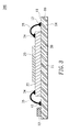
- Fig. 1B is a schematic view illustrating tilting and consequent fracture of a transparent window during a process of manufacturing the conventional image sensor.
- Fig. 1C is a schematic view illustrating tilting of the transparent window and consequent overflow of an adhesive during the process of manufacturing the conventional image sensor.
- the conventional image sensor 100 substantially includes a circuit substrate 10 (e.g., a printed circuit board; PCB), an image sensor die 20, a transparent window 30 and an encapsulant 40.
- the image sensor die 20 is disposed on the circuit substrate 10 and is electrically connected to circuits on the circuit substrate 10 via metal wirings 25 through wire bonding, and the transparent window 30 is disposed above a photosensitive region (not shown) of the image sensor die 20 by means of an adhesive 26 such as an epoxy resin, and then the metal wirings 25 and side edges of the image sensing die 20 and the transparent window 30 are encapsulated by the encapsulant 40 through molding.
- an adhesive 26 such as an epoxy resin
- the transparent window 30 adhered above the photosensitive region (not shown) of the image sensing die 20 is placed in an out-of-level state (e.g., inclined in the lateral direction) during the molding process, then the tilt of the transparent window 30 with respect to the image sensor die 20 or the circuit substrate 10 will become overly large and this makes it easy to cause fracture of the transparent window 30 when the mold 50 is pressed downwards during the molding process, which decreases the yield rate of image sensors.
- an out-of-level state e.g., inclined in the lateral direction
- the air in a space enclosed by the transparent window 30, the image sensor die 20 and the adhesive 26 during the molding process tends to expand non-uniformly when heated by a high environmental temperature. This will not only push the transparent window 30 to cause tilting of the transparent window 30 but also push the adhesive 26 outwards to cause overflow of the adhesive 26, thus degrading the yield rate of image sensors.
- the present invention is a method for reducing the tilt of a transparent window during manufacturing of an image sensor.
- a preheating process is carried out to release the air pressure inside a space in the vicinity of the image sensor die so that the enclosed space formed when the transparent window is closed will not expand at the high temperature of subsequent processes to cause unevenness of the transparent window.
- the tilt of the transparent window can be reduced and fracture of the transparent window during the transparent window closing process can be avoided, thus improving the yield rate.
- the present invention provides A method for reducing the tilt of a transparent window during manufacturing of an image sensor, comprising the following steps: providing a semimanufacture of the image sensor, which comprises a circuit substrate and an image sensor die, wherein the circuit substrate has a supporting surface and a bottom surface, a plurality of first conductive contacts are provided on the supporting surface, and the image sensor die comprises: a first surface attached to the supporting surface; a second surface having a photosensitive region; and a plurality of second conductive contacts disposed outside the photosensitive region and electrically connected to the first conductive contacts via metal wirings respectively; carrying out a preheating process by placing the semimanufacture into an environment at a specific temperature; carrying out an adhesive spreading process by, after the preheating process, spreading an adhesive onto the second surface around the photosensitive region without covering the photosensitive region; carrying out a transparent window closing process by, after the adhesive spreading process, placing a transparent window on the adhesive and curing the adhesive to fix the transparent window onto the second surface and to form an air chamber between the image sensor
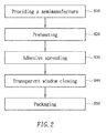
- this embodiment is a method for reducing the tilt of a transparent window during manufacturing of an image sensor, which comprises the following steps of: providing a semimanfuacture (step S10); carrying out a preheating process (step S20); carrying out an adhesive spreading process (step S30); carrying out a transparent window closing process (step S40); and carrying out a packaging process (step S50).
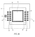
- the semimanufacture 200 provided in this embodiment is a semimanufacture of an image sensor, which comprises a circuit substrate 10 and an image sensor die 20.
- the circuit substrate 10 has a supporting surface 11 and a bottom surface 14.
- a plurality of first conductive pads 12 is disposed on the supporting surface 11 for electrical connection in the wire bonding process and the plurality of first conductive pads is electrically connected to circuits on the supporting surface 11.
- a drive integrated circuit (IC) and passive elements 13 may also be optionally disposed on the supporting surface 11 and electrically connected to the circuits on the supporting surface 11.
- the image sensor die 20 may be a complementary metal oxide semiconductor (CMOS) image sensor die or a charge coupled device (CCE), and comprises: a first surface 21; a second surface 22; and a plurality of second conductive contacts 24.
- CMOS complementary metal oxide semiconductor
- CCE charge coupled device
- the first surface 21 is the lower surface of the image sensor die 20, and is attached to the supporting surface 11 through use of an adhesive so that the image sensor die 20 is attached to the circuit substrate 10.
- the second surface 22 is the upper surface of the image sensor die 20, and has a photosensitive region 23 for receiving and sensing light rays.
- the second conductive contacts 24 are disposed outside the photosensitive region 23 and electrically connected to the first conductive contacts 12 on the first surface 21 by metal wirings 25 respectively.
- the image sensor die 20 can be electrically connected to the drive 1C and the passive elements 13 through the circuits on the supporting surface 11.
- a preheating process is carried out (step S20) by placing the semimanufacture 200 into an environment at a specific temperature.
- the environment at the specific temperature may be an oven, and the specific temperature may range between 35°C and 45°C.
- the air temperature around the second surface 22 and the supporting surface 11 can be increased to a temperature range which is the same as the environment temperature in the subsequent adhesive spreading process and the subsequent transparent window closing process so as to release the air pressure in the space around the second surface 22 and the supporting surface 11.
- This can prevent the air around the second surface 22 and the supporting surface 11 from being influenced by the temperature rise in the subsequent adhesive spreading process or the subsequent transparent window closing process to cause non-uniform expansion and consequent tilting of the transparent window (not shown).
- This can also prevent the enclosed space formed in the transparent window closing process from expanding due to the temperature rise to cause unevenness of the transparent window, and prevent occurrence of overflow of the adhesive.
- an adhesive spreading process is carried out (step S30) after the preheating process (step S20) by spreading an adhesive 26 onto the second surface 22 around the photosensitive region 23 without covering the photosensitive region 23.
- the environment temperature may still be maintained at the specific temperature which is the same as that of the preheating process (e.g., between 35°C and 45°C).
- the adhesive 26 may be applied in regions between the photosensitive region 23 and the second conductive contacts 24 to form a ⁇ -shaped pattern, which looks like a frame-shaped pattern.
- the photosensitive region 23 after being packaged can be accommodated in the space formed by the adhesive 26 and the transparent window (not shown) to prevent the photosensitive region 23 from being influenced by external factors.
- a plurality of ball spacers 27 may be further added into the adhesive 26 to keep a most appropriate distance between the transparent window (not shown) and the image sensing die 20 so that the tilt of the transparent window (not shown) is controlled to be within a reasonable range.
- a transparent window closing process (step S40) is carried out.
- the transparent window 30 may be a glass board.
- the transparent window closing process is carried out after the adhesive spreading process (S30) by placing the transparent window 30 on the adhesive 26 and curing the adhesive 26 to fix the transparent window 30 onto the second surface 22 and to form an air chamber 31 between the image sensor die 20 and the transparent window 30.
- the environment temperature may also be maintained at the specific temperature which is the same as that of the preheating process (e.g., between 35°C and 45°C).
- the adhesive 26 may be a photocurable adhesive, and particularly an ultraviolet (UV) curable adhesive; and in the transparent window closing process, the UV curable adhesive is cured through irradiation of UV light rays.
- UV ultraviolet
- a packaging process (step S50) is carried out by packaging the semimanufacture and the transparent window 30 with an encapsulant 40 through use of a molding process or a dispensing technology.
- the encapsulant 40 may be applied to cover side edges of the semimanufacture, the adhesive 26 and the transparent window 30. More specifically, a space formed by side edges of the transparent window 30 and a bottom surface of the transparent window 30, side edges of the circuit substrate 10 and a top surface of the circuit substrate 10, and the periphery of the ⁇ -shaped region applied with the adhesive 26 may be encapsulated by the encapsulant 40.
- the encapsulant 40 may be used to cover the side edges of the circuit substrate 10, the side edges of the circuit substrate 10 can be prevented from being damaged due to impacts.
- the encapsulant 40 may also be disposed on the circuit substrate 10 and cover the side edges of the image sensor die 20, the adhesive 26 and the transparent window 30. More specifically, a space formed by side edges of the transparent window 30 and the bottom surface of the transparent window 30, the top surface of the circuit substrate 10 (but except for the side edges of the circuit substrate 10) and the periphery of the ⁇ -shaped region applied with the adhesive 26 may be encapsulated by the encapsulant 40.
- semimanufactures 200 that have been subjected to the transparent window closing process may also be arranged on a base 62 of a large-scale packaging mold 600, and then a top cover 61 of the large-scale packaging mold 600 is joined with the base 62 to carry out the packaging process (step S50) so as to achieve the purpose of mass production.
Landscapes
- Solid State Image Pick-Up Elements (AREA)
- Transforming Light Signals Into Electric Signals (AREA)
- Encapsulation Of And Coatings For Semiconductor Or Solid State Devices (AREA)
Priority Applications (1)
| Application Number | Priority Date | Filing Date | Title |
|---|---|---|---|
| EP13154912.3A EP2629331B1 (fr) | 2011-02-24 | 2013-02-12 | Procédé pour réduire l'inclinaison d'une fenêtre transparente pendant la fabrication d'un capteur d'image |
Applications Claiming Priority (1)
| Application Number | Priority Date | Filing Date | Title |
|---|---|---|---|
| US201161446355P | 2011-02-24 | 2011-02-24 |
Publications (3)
| Publication Number | Publication Date |
|---|---|
| EP2492961A2 true EP2492961A2 (fr) | 2012-08-29 |
| EP2492961A3 EP2492961A3 (fr) | 2013-04-03 |
| EP2492961B1 EP2492961B1 (fr) | 2014-04-09 |
Family
ID=45655986
Family Applications (2)
| Application Number | Title | Priority Date | Filing Date |
|---|---|---|---|
| EP12155846.4A Not-in-force EP2492961B1 (fr) | 2011-02-24 | 2012-02-16 | Procédé pour réduire l'inclinaison d'une fenêtre transparente pendant la fabrication d'un capteur d'image |
| EP13154912.3A Not-in-force EP2629331B1 (fr) | 2011-02-24 | 2013-02-12 | Procédé pour réduire l'inclinaison d'une fenêtre transparente pendant la fabrication d'un capteur d'image |
Family Applications After (1)
| Application Number | Title | Priority Date | Filing Date |
|---|---|---|---|
| EP13154912.3A Not-in-force EP2629331B1 (fr) | 2011-02-24 | 2013-02-12 | Procédé pour réduire l'inclinaison d'une fenêtre transparente pendant la fabrication d'un capteur d'image |
Country Status (5)
| Country | Link |
|---|---|
| US (1) | US8450137B2 (fr) |
| EP (2) | EP2492961B1 (fr) |
| JP (2) | JP2012178564A (fr) |
| CN (1) | CN102651374B (fr) |
| TW (1) | TWI414062B (fr) |
Cited By (1)
| Publication number | Priority date | Publication date | Assignee | Title |
|---|---|---|---|---|
| EP3267486A1 (fr) * | 2016-07-06 | 2018-01-10 | Kingpak Technology Inc. | Structure de boîtier de capteur |
Families Citing this family (9)
| Publication number | Priority date | Publication date | Assignee | Title |
|---|---|---|---|---|
| TWI495097B (zh) * | 2012-02-02 | 2015-08-01 | Kingpak Tech Inc | 降低光學單元傾斜度之影像感測器製造方法 |
| WO2014083750A1 (fr) * | 2012-11-30 | 2014-06-05 | パナソニック株式会社 | Appareil optique et son procédé de fabrication |
| TWM455258U (zh) * | 2013-01-11 | 2013-06-11 | 勝開科技股份有限公司 | 具有氣室缺口之影像感測器結構 |
| CN103943640A (zh) * | 2013-01-22 | 2014-07-23 | 胜开科技股份有限公司 | 降低光学单元倾斜度的影像感测器制造方法 |
| CN104427215A (zh) * | 2013-08-29 | 2015-03-18 | 光宝科技股份有限公司 | 图像获取模块 |
| CN104754930A (zh) * | 2013-12-27 | 2015-07-01 | 鸿富锦精密工业(深圳)有限公司 | 电子装置的重工方法 |
| TWI503589B (zh) * | 2014-04-23 | 2015-10-11 | 用於增加組裝平整度且降低調焦時間的影像擷取模組及其組裝方法 | |
| KR20220051470A (ko) * | 2020-10-19 | 2022-04-26 | 삼성전자주식회사 | 반도체 패키지 및 이의 제조 방법 |
| TWI840150B (zh) * | 2022-10-17 | 2024-04-21 | 同欣電子工業股份有限公司 | 感測器封裝結構及其製造方法 |
Family Cites Families (14)
| Publication number | Priority date | Publication date | Assignee | Title |
|---|---|---|---|---|
| JPH05191733A (ja) * | 1992-01-16 | 1993-07-30 | Hitachi Ltd | 固体撮像装置 |
| US6428650B1 (en) * | 1998-06-23 | 2002-08-06 | Amerasia International Technology, Inc. | Cover for an optical device and method for making same |
| TW521410B (en) * | 2001-11-15 | 2003-02-21 | Siliconware Precision Industries Co Ltd | Semiconductor package article |
| JP2004296453A (ja) * | 2003-02-06 | 2004-10-21 | Sharp Corp | 固体撮像装置、半導体ウエハ、光学装置用モジュール、固体撮像装置の製造方法及び光学装置用モジュールの製造方法 |
| US6874227B2 (en) * | 2003-06-03 | 2005-04-05 | Kingpak Technology Inc. | Method for packaging an image sensor |
| JP4198072B2 (ja) * | 2004-01-23 | 2008-12-17 | シャープ株式会社 | 半導体装置、光学装置用モジュール及び半導体装置の製造方法 |
| US7863702B2 (en) * | 2004-06-10 | 2011-01-04 | Samsung Electronics Co., Ltd. | Image sensor package and method of manufacturing the same |
| TWI333249B (en) * | 2004-08-24 | 2010-11-11 | Himax Tech Inc | Sensor package |
| TWI248665B (en) * | 2004-12-06 | 2006-02-01 | Chipmos Technologies Inc | Image sensor package and method for manufacturing the same |
| CN1873992A (zh) * | 2005-06-03 | 2006-12-06 | 鸿富锦精密工业(深圳)有限公司 | 影像感测器封装和封装制程 |
| JP2008029916A (ja) * | 2006-07-26 | 2008-02-14 | Dainippon Printing Co Ltd | 凸形状パターン形成方法とセンサーチップの製造装置および製造方法 |
| TW201103128A (en) * | 2009-07-03 | 2011-01-16 | Creative Sensor Inc | Image sensor and the method for package of the same |
| JP2011060974A (ja) * | 2009-09-09 | 2011-03-24 | Canon Inc | 固体撮像装置及びデジタルカメラ |
| JP2011238667A (ja) * | 2010-05-06 | 2011-11-24 | Shinko Electric Ind Co Ltd | 固体撮像装置の製造方法および固体撮像装置 |
-
2012
- 2012-02-02 TW TW101103436A patent/TWI414062B/zh not_active IP Right Cessation
- 2012-02-13 CN CN201210031502.1A patent/CN102651374B/zh not_active Expired - Fee Related
- 2012-02-16 EP EP12155846.4A patent/EP2492961B1/fr not_active Not-in-force
- 2012-02-20 JP JP2012034329A patent/JP2012178564A/ja active Pending
- 2012-02-23 US US13/403,159 patent/US8450137B2/en not_active Expired - Fee Related
-
2013
- 2013-02-05 JP JP2013020295A patent/JP5552548B2/ja not_active Expired - Fee Related
- 2013-02-12 EP EP13154912.3A patent/EP2629331B1/fr not_active Not-in-force
Non-Patent Citations (1)
| Title |
|---|
| None |
Cited By (1)
| Publication number | Priority date | Publication date | Assignee | Title |
|---|---|---|---|---|
| EP3267486A1 (fr) * | 2016-07-06 | 2018-01-10 | Kingpak Technology Inc. | Structure de boîtier de capteur |
Also Published As
| Publication number | Publication date |
|---|---|
| US20120220065A1 (en) | 2012-08-30 |
| EP2629331B1 (fr) | 2014-05-14 |
| CN102651374B (zh) | 2014-09-24 |
| CN102651374A (zh) | 2012-08-29 |
| US8450137B2 (en) | 2013-05-28 |
| JP5552548B2 (ja) | 2014-07-16 |
| JP2012178564A (ja) | 2012-09-13 |
| TW201236148A (en) | 2012-09-01 |
| EP2492961A3 (fr) | 2013-04-03 |
| TWI414062B (zh) | 2013-11-01 |
| JP2013201423A (ja) | 2013-10-03 |
| EP2629331A1 (fr) | 2013-08-21 |
| EP2492961B1 (fr) | 2014-04-09 |
Similar Documents
| Publication | Publication Date | Title |
|---|---|---|
| US8450137B2 (en) | Method for reducing tilt of transparent window during manufacturing of image sensor | |
| US9184331B2 (en) | Method for reducing tilt of optical unit during manufacture of image sensor | |
| EP2375446B1 (fr) | Structure d'emballage de capteur d'image au niveau plaque et son procédé de fabrication | |
| CN102891152B (zh) | 半导体封装体 | |
| TWI398949B (zh) | 模造成型之影像感測器封裝結構製造方法及封裝結構 | |
| CN106601727B (zh) | 包模接近度传感器及相关联的方法 | |
| US20160141232A1 (en) | Integrated circuit package | |
| US8816212B2 (en) | Flexible device and fabricating method thereof | |
| KR200473633Y1 (ko) | 챔버 개구를 가지는 이미지 센서 구조 | |
| CN113196477B (zh) | 具有光发射器和光接收器的光电模块 | |
| US10510932B2 (en) | Optoelectronic modules including optoelectronic device subassemblies and methods of manufacturing the same | |
| US12169315B2 (en) | Optoelectronic modules and wafer-level methods for manufacturing the same | |
| KR20130089601A (ko) | 광학 유닛의 경사도를 감소시키는 이미지 센서의 제조방법 | |
| CN103943640A (zh) | 降低光学单元倾斜度的影像感测器制造方法 | |
| TWI495097B (zh) | 降低光學單元傾斜度之影像感測器製造方法 | |
| CN204243030U (zh) | 一种电子器件 | |
| CN121096966A (zh) | 封装结构及其制造方法 | |
| JP2008028238A (ja) | 固体撮像素子の気密封止方法 | |
| KR20090010319U (ko) | 반도체 패키지 제조용 장치 |
Legal Events
| Date | Code | Title | Description |
|---|---|---|---|
| PUAI | Public reference made under article 153(3) epc to a published international application that has entered the european phase |
Free format text: ORIGINAL CODE: 0009012 |
|
| AK | Designated contracting states |
Kind code of ref document: A2 Designated state(s): AL AT BE BG CH CY CZ DE DK EE ES FI FR GB GR HR HU IE IS IT LI LT LU LV MC MK MT NL NO PL PT RO RS SE SI SK SM TR |
|
| AX | Request for extension of the european patent |
Extension state: BA ME |
|
| PUAL | Search report despatched |
Free format text: ORIGINAL CODE: 0009013 |
|
| AK | Designated contracting states |
Kind code of ref document: A3 Designated state(s): AL AT BE BG CH CY CZ DE DK EE ES FI FR GB GR HR HU IE IS IT LI LT LU LV MC MK MT NL NO PL PT RO RS SE SI SK SM TR |
|
| AX | Request for extension of the european patent |
Extension state: BA ME |
|
| RIC1 | Information provided on ipc code assigned before grant |
Ipc: H01L 27/146 20060101AFI20130228BHEP |
|
| 17P | Request for examination filed |
Effective date: 20130422 |
|
| GRAP | Despatch of communication of intention to grant a patent |
Free format text: ORIGINAL CODE: EPIDOSNIGR1 |
|
| INTG | Intention to grant announced |
Effective date: 20131014 |
|
| GRAS | Grant fee paid |
Free format text: ORIGINAL CODE: EPIDOSNIGR3 |
|
| GRAA | (expected) grant |
Free format text: ORIGINAL CODE: 0009210 |
|
| AK | Designated contracting states |
Kind code of ref document: B1 Designated state(s): AL AT BE BG CH CY CZ DE DK EE ES FI FR GB GR HR HU IE IS IT LI LT LU LV MC MK MT NL NO PL PT RO RS SE SI SK SM TR |
|
| REG | Reference to a national code |
Ref country code: GB Ref legal event code: FG4D |
|
| REG | Reference to a national code |
Ref country code: AT Ref legal event code: REF Ref document number: 661759 Country of ref document: AT Kind code of ref document: T Effective date: 20140415 Ref country code: CH Ref legal event code: EP |
|
| REG | Reference to a national code |
Ref country code: IE Ref legal event code: FG4D |
|
| REG | Reference to a national code |
Ref country code: DE Ref legal event code: R096 Ref document number: 602012001326 Country of ref document: DE Effective date: 20140522 |
|
| REG | Reference to a national code |
Ref country code: AT Ref legal event code: MK05 Ref document number: 661759 Country of ref document: AT Kind code of ref document: T Effective date: 20140409 |
|
| REG | Reference to a national code |
Ref country code: NL Ref legal event code: VDEP Effective date: 20140409 |
|
| REG | Reference to a national code |
Ref country code: LT Ref legal event code: MG4D |
|
| PG25 | Lapsed in a contracting state [announced via postgrant information from national office to epo] |
Ref country code: BG Free format text: LAPSE BECAUSE OF FAILURE TO SUBMIT A TRANSLATION OF THE DESCRIPTION OR TO PAY THE FEE WITHIN THE PRESCRIBED TIME-LIMIT Effective date: 20140709 Ref country code: NL Free format text: LAPSE BECAUSE OF FAILURE TO SUBMIT A TRANSLATION OF THE DESCRIPTION OR TO PAY THE FEE WITHIN THE PRESCRIBED TIME-LIMIT Effective date: 20140409 Ref country code: GR Free format text: LAPSE BECAUSE OF FAILURE TO SUBMIT A TRANSLATION OF THE DESCRIPTION OR TO PAY THE FEE WITHIN THE PRESCRIBED TIME-LIMIT Effective date: 20140710 Ref country code: FI Free format text: LAPSE BECAUSE OF FAILURE TO SUBMIT A TRANSLATION OF THE DESCRIPTION OR TO PAY THE FEE WITHIN THE PRESCRIBED TIME-LIMIT Effective date: 20140409 Ref country code: IS Free format text: LAPSE BECAUSE OF FAILURE TO SUBMIT A TRANSLATION OF THE DESCRIPTION OR TO PAY THE FEE WITHIN THE PRESCRIBED TIME-LIMIT Effective date: 20140809 Ref country code: NO Free format text: LAPSE BECAUSE OF FAILURE TO SUBMIT A TRANSLATION OF THE DESCRIPTION OR TO PAY THE FEE WITHIN THE PRESCRIBED TIME-LIMIT Effective date: 20140709 Ref country code: LT Free format text: LAPSE BECAUSE OF FAILURE TO SUBMIT A TRANSLATION OF THE DESCRIPTION OR TO PAY THE FEE WITHIN THE PRESCRIBED TIME-LIMIT Effective date: 20140409 |
|
| PG25 | Lapsed in a contracting state [announced via postgrant information from national office to epo] |
Ref country code: SE Free format text: LAPSE BECAUSE OF FAILURE TO SUBMIT A TRANSLATION OF THE DESCRIPTION OR TO PAY THE FEE WITHIN THE PRESCRIBED TIME-LIMIT Effective date: 20140409 Ref country code: HR Free format text: LAPSE BECAUSE OF FAILURE TO SUBMIT A TRANSLATION OF THE DESCRIPTION OR TO PAY THE FEE WITHIN THE PRESCRIBED TIME-LIMIT Effective date: 20140409 Ref country code: PL Free format text: LAPSE BECAUSE OF FAILURE TO SUBMIT A TRANSLATION OF THE DESCRIPTION OR TO PAY THE FEE WITHIN THE PRESCRIBED TIME-LIMIT Effective date: 20140409 Ref country code: LV Free format text: LAPSE BECAUSE OF FAILURE TO SUBMIT A TRANSLATION OF THE DESCRIPTION OR TO PAY THE FEE WITHIN THE PRESCRIBED TIME-LIMIT Effective date: 20140409 Ref country code: ES Free format text: LAPSE BECAUSE OF FAILURE TO SUBMIT A TRANSLATION OF THE DESCRIPTION OR TO PAY THE FEE WITHIN THE PRESCRIBED TIME-LIMIT Effective date: 20140409 Ref country code: RS Free format text: LAPSE BECAUSE OF FAILURE TO SUBMIT A TRANSLATION OF THE DESCRIPTION OR TO PAY THE FEE WITHIN THE PRESCRIBED TIME-LIMIT Effective date: 20140409 Ref country code: AT Free format text: LAPSE BECAUSE OF FAILURE TO SUBMIT A TRANSLATION OF THE DESCRIPTION OR TO PAY THE FEE WITHIN THE PRESCRIBED TIME-LIMIT Effective date: 20140409 |
|
| PG25 | Lapsed in a contracting state [announced via postgrant information from national office to epo] |
Ref country code: PT Free format text: LAPSE BECAUSE OF FAILURE TO SUBMIT A TRANSLATION OF THE DESCRIPTION OR TO PAY THE FEE WITHIN THE PRESCRIBED TIME-LIMIT Effective date: 20140811 |
|
| REG | Reference to a national code |
Ref country code: DE Ref legal event code: R097 Ref document number: 602012001326 Country of ref document: DE |
|
| PG25 | Lapsed in a contracting state [announced via postgrant information from national office to epo] |
Ref country code: CZ Free format text: LAPSE BECAUSE OF FAILURE TO SUBMIT A TRANSLATION OF THE DESCRIPTION OR TO PAY THE FEE WITHIN THE PRESCRIBED TIME-LIMIT Effective date: 20140409 Ref country code: EE Free format text: LAPSE BECAUSE OF FAILURE TO SUBMIT A TRANSLATION OF THE DESCRIPTION OR TO PAY THE FEE WITHIN THE PRESCRIBED TIME-LIMIT Effective date: 20140409 Ref country code: SK Free format text: LAPSE BECAUSE OF FAILURE TO SUBMIT A TRANSLATION OF THE DESCRIPTION OR TO PAY THE FEE WITHIN THE PRESCRIBED TIME-LIMIT Effective date: 20140409 Ref country code: DK Free format text: LAPSE BECAUSE OF FAILURE TO SUBMIT A TRANSLATION OF THE DESCRIPTION OR TO PAY THE FEE WITHIN THE PRESCRIBED TIME-LIMIT Effective date: 20140409 Ref country code: RO Free format text: LAPSE BECAUSE OF FAILURE TO SUBMIT A TRANSLATION OF THE DESCRIPTION OR TO PAY THE FEE WITHIN THE PRESCRIBED TIME-LIMIT Effective date: 20140409 Ref country code: BE Free format text: LAPSE BECAUSE OF FAILURE TO SUBMIT A TRANSLATION OF THE DESCRIPTION OR TO PAY THE FEE WITHIN THE PRESCRIBED TIME-LIMIT Effective date: 20140409 |
|
| PLBE | No opposition filed within time limit |
Free format text: ORIGINAL CODE: 0009261 |
|
| STAA | Information on the status of an ep patent application or granted ep patent |
Free format text: STATUS: NO OPPOSITION FILED WITHIN TIME LIMIT |
|
| REG | Reference to a national code |
Ref country code: FR Ref legal event code: PLFP Year of fee payment: 4 |
|
| 26N | No opposition filed |
Effective date: 20150112 |
|
| PG25 | Lapsed in a contracting state [announced via postgrant information from national office to epo] |
Ref country code: IT Free format text: LAPSE BECAUSE OF FAILURE TO SUBMIT A TRANSLATION OF THE DESCRIPTION OR TO PAY THE FEE WITHIN THE PRESCRIBED TIME-LIMIT Effective date: 20140409 |
|
| REG | Reference to a national code |
Ref country code: DE Ref legal event code: R097 Ref document number: 602012001326 Country of ref document: DE Effective date: 20150112 |
|
| PGFP | Annual fee paid to national office [announced via postgrant information from national office to epo] |
Ref country code: DE Payment date: 20150130 Year of fee payment: 4 |
|
| PGFP | Annual fee paid to national office [announced via postgrant information from national office to epo] |
Ref country code: FR Payment date: 20150217 Year of fee payment: 4 |
|
| PG25 | Lapsed in a contracting state [announced via postgrant information from national office to epo] |
Ref country code: SI Free format text: LAPSE BECAUSE OF FAILURE TO SUBMIT A TRANSLATION OF THE DESCRIPTION OR TO PAY THE FEE WITHIN THE PRESCRIBED TIME-LIMIT Effective date: 20140409 |
|
| PG25 | Lapsed in a contracting state [announced via postgrant information from national office to epo] |
Ref country code: LU Free format text: LAPSE BECAUSE OF FAILURE TO SUBMIT A TRANSLATION OF THE DESCRIPTION OR TO PAY THE FEE WITHIN THE PRESCRIBED TIME-LIMIT Effective date: 20150216 |
|
| REG | Reference to a national code |
Ref country code: CH Ref legal event code: PL |
|
| PG25 | Lapsed in a contracting state [announced via postgrant information from national office to epo] |
Ref country code: LI Free format text: LAPSE BECAUSE OF NON-PAYMENT OF DUE FEES Effective date: 20150228 Ref country code: CH Free format text: LAPSE BECAUSE OF NON-PAYMENT OF DUE FEES Effective date: 20150228 Ref country code: MC Free format text: LAPSE BECAUSE OF FAILURE TO SUBMIT A TRANSLATION OF THE DESCRIPTION OR TO PAY THE FEE WITHIN THE PRESCRIBED TIME-LIMIT Effective date: 20140409 |
|
| REG | Reference to a national code |
Ref country code: IE Ref legal event code: MM4A |
|
| PG25 | Lapsed in a contracting state [announced via postgrant information from national office to epo] |
Ref country code: IE Free format text: LAPSE BECAUSE OF NON-PAYMENT OF DUE FEES Effective date: 20150216 |
|
| REG | Reference to a national code |
Ref country code: DE Ref legal event code: R119 Ref document number: 602012001326 Country of ref document: DE |
|
| GBPC | Gb: european patent ceased through non-payment of renewal fee |
Effective date: 20160216 |
|
| REG | Reference to a national code |
Ref country code: FR Ref legal event code: ST Effective date: 20161028 |
|
| PG25 | Lapsed in a contracting state [announced via postgrant information from national office to epo] |
Ref country code: MT Free format text: LAPSE BECAUSE OF FAILURE TO SUBMIT A TRANSLATION OF THE DESCRIPTION OR TO PAY THE FEE WITHIN THE PRESCRIBED TIME-LIMIT Effective date: 20140409 |
|
| PG25 | Lapsed in a contracting state [announced via postgrant information from national office to epo] |
Ref country code: DE Free format text: LAPSE BECAUSE OF NON-PAYMENT OF DUE FEES Effective date: 20160901 Ref country code: FR Free format text: LAPSE BECAUSE OF NON-PAYMENT OF DUE FEES Effective date: 20160229 Ref country code: GB Free format text: LAPSE BECAUSE OF NON-PAYMENT OF DUE FEES Effective date: 20160216 |
|
| PG25 | Lapsed in a contracting state [announced via postgrant information from national office to epo] |
Ref country code: SM Free format text: LAPSE BECAUSE OF FAILURE TO SUBMIT A TRANSLATION OF THE DESCRIPTION OR TO PAY THE FEE WITHIN THE PRESCRIBED TIME-LIMIT Effective date: 20140409 Ref country code: HU Free format text: LAPSE BECAUSE OF FAILURE TO SUBMIT A TRANSLATION OF THE DESCRIPTION OR TO PAY THE FEE WITHIN THE PRESCRIBED TIME-LIMIT; INVALID AB INITIO Effective date: 20120216 |
|
| PG25 | Lapsed in a contracting state [announced via postgrant information from national office to epo] |
Ref country code: CY Free format text: LAPSE BECAUSE OF FAILURE TO SUBMIT A TRANSLATION OF THE DESCRIPTION OR TO PAY THE FEE WITHIN THE PRESCRIBED TIME-LIMIT Effective date: 20140409 |
|
| PG25 | Lapsed in a contracting state [announced via postgrant information from national office to epo] |
Ref country code: TR Free format text: LAPSE BECAUSE OF FAILURE TO SUBMIT A TRANSLATION OF THE DESCRIPTION OR TO PAY THE FEE WITHIN THE PRESCRIBED TIME-LIMIT Effective date: 20140409 |
|
| PG25 | Lapsed in a contracting state [announced via postgrant information from national office to epo] |
Ref country code: MK Free format text: LAPSE BECAUSE OF FAILURE TO SUBMIT A TRANSLATION OF THE DESCRIPTION OR TO PAY THE FEE WITHIN THE PRESCRIBED TIME-LIMIT Effective date: 20140409 |
|
| PG25 | Lapsed in a contracting state [announced via postgrant information from national office to epo] |
Ref country code: AL Free format text: LAPSE BECAUSE OF FAILURE TO SUBMIT A TRANSLATION OF THE DESCRIPTION OR TO PAY THE FEE WITHIN THE PRESCRIBED TIME-LIMIT Effective date: 20140409 |