EP2498052A2 - Hochlinearer Signalverarbeitungsverstärker - Google Patents
Hochlinearer Signalverarbeitungsverstärker Download PDFInfo
- Publication number
- EP2498052A2 EP2498052A2 EP12157997A EP12157997A EP2498052A2 EP 2498052 A2 EP2498052 A2 EP 2498052A2 EP 12157997 A EP12157997 A EP 12157997A EP 12157997 A EP12157997 A EP 12157997A EP 2498052 A2 EP2498052 A2 EP 2498052A2
- Authority
- EP
- European Patent Office
- Prior art keywords
- junction transistor
- circuit
- bipolar junction
- rate
- output
- Prior art date
- Legal status (The legal status is an assumption and is not a legal conclusion. Google has not performed a legal analysis and makes no representation as to the accuracy of the status listed.)
- Granted
Links
Images




Classifications
-
- G—PHYSICS
- G01—MEASURING; TESTING
- G01C—MEASURING DISTANCES, LEVELS OR BEARINGS; SURVEYING; NAVIGATION; GYROSCOPIC INSTRUMENTS; PHOTOGRAMMETRY OR VIDEOGRAMMETRY
- G01C19/00—Gyroscopes; Turn-sensitive devices using vibrating masses; Turn-sensitive devices without moving masses; Measuring angular rate using gyroscopic effects
- G01C19/58—Turn-sensitive devices without moving masses
- G01C19/64—Gyrometers using the Sagnac effect, i.e. rotation-induced shifts between counter-rotating electromagnetic beams
- G01C19/72—Gyrometers using the Sagnac effect, i.e. rotation-induced shifts between counter-rotating electromagnetic beams with counter-rotating light beams in a passive ring, e.g. fibre laser gyrometers
- G01C19/721—Details, e.g. optical or electronical details
-
- G—PHYSICS
- G01—MEASURING; TESTING
- G01J—MEASUREMENT OF INTENSITY, VELOCITY, SPECTRAL CONTENT, POLARISATION, PHASE OR PULSE CHARACTERISTICS OF INFRARED, VISIBLE OR ULTRAVIOLET LIGHT; COLORIMETRY; RADIATION PYROMETRY
- G01J1/00—Photometry, e.g. photographic exposure meter
- G01J1/42—Photometry, e.g. photographic exposure meter using electric radiation detectors
- G01J1/44—Electric circuits
- G01J1/46—Electric circuits using a capacitor
-
- H—ELECTRICITY
- H03—ELECTRONIC CIRCUITRY
- H03F—AMPLIFIERS
- H03F1/00—Details of amplifiers with only discharge tubes, only semiconductor devices or only unspecified devices as amplifying elements
- H03F1/32—Modifications of amplifiers to reduce non-linear distortion
- H03F1/3211—Modifications of amplifiers to reduce non-linear distortion in differential amplifiers
-
- H—ELECTRICITY
- H03—ELECTRONIC CIRCUITRY
- H03F—AMPLIFIERS
- H03F3/00—Amplifiers with only discharge tubes or only semiconductor devices as amplifying elements
- H03F3/04—Amplifiers with only discharge tubes or only semiconductor devices as amplifying elements with semiconductor devices only
- H03F3/08—Amplifiers with only discharge tubes or only semiconductor devices as amplifying elements with semiconductor devices only controlled by light
- H03F3/087—Amplifiers with only discharge tubes or only semiconductor devices as amplifying elements with semiconductor devices only controlled by light with IC amplifier blocks
-
- H—ELECTRICITY
- H03—ELECTRONIC CIRCUITRY
- H03F—AMPLIFIERS
- H03F3/00—Amplifiers with only discharge tubes or only semiconductor devices as amplifying elements
- H03F3/45—Differential amplifiers
- H03F3/45071—Differential amplifiers with semiconductor devices only
- H03F3/45076—Differential amplifiers with semiconductor devices only characterised by the way of implementation of the active amplifying circuit in the differential amplifier
- H03F3/45475—Differential amplifiers with semiconductor devices only characterised by the way of implementation of the active amplifying circuit in the differential amplifier using IC blocks as the active amplifying circuit
-
- H—ELECTRICITY
- H03—ELECTRONIC CIRCUITRY
- H03G—CONTROL OF AMPLIFICATION
- H03G11/00—Limiting amplitude; Limiting rate of change of amplitude
- H03G11/02—Limiting amplitude; Limiting rate of change of amplitude by means of diodes
-
- H—ELECTRICITY
- H03—ELECTRONIC CIRCUITRY
- H03F—AMPLIFIERS
- H03F2200/00—Indexing scheme relating to amplifiers
- H03F2200/261—Amplifier which being suitable for instrumentation applications
-
- H—ELECTRICITY
- H03—ELECTRONIC CIRCUITRY
- H03F—AMPLIFIERS
- H03F2203/00—Indexing scheme relating to amplifiers with only discharge tubes or only semiconductor devices as amplifying elements covered by H03F3/00
- H03F2203/45—Indexing scheme relating to differential amplifiers
- H03F2203/45512—Indexing scheme relating to differential amplifiers the FBC comprising one or more capacitors, not being switched capacitors, and being coupled between the LC and the IC
-
- H—ELECTRICITY
- H03—ELECTRONIC CIRCUITRY
- H03F—AMPLIFIERS
- H03F2203/00—Indexing scheme relating to amplifiers with only discharge tubes or only semiconductor devices as amplifying elements covered by H03F3/00
- H03F2203/45—Indexing scheme relating to differential amplifiers
- H03F2203/45518—Indexing scheme relating to differential amplifiers the FBC comprising one or more diodes and being coupled between the LC and the IC
-
- H—ELECTRICITY
- H03—ELECTRONIC CIRCUITRY
- H03F—AMPLIFIERS
- H03F2203/00—Indexing scheme relating to amplifiers with only discharge tubes or only semiconductor devices as amplifying elements covered by H03F3/00
- H03F2203/45—Indexing scheme relating to differential amplifiers
- H03F2203/45528—Indexing scheme relating to differential amplifiers the FBC comprising one or more passive resistors and being coupled between the LC and the IC
-
- H—ELECTRICITY
- H03—ELECTRONIC CIRCUITRY
- H03F—AMPLIFIERS
- H03F2203/00—Indexing scheme relating to amplifiers with only discharge tubes or only semiconductor devices as amplifying elements covered by H03F3/00
- H03F2203/45—Indexing scheme relating to differential amplifiers
- H03F2203/45594—Indexing scheme relating to differential amplifiers the IC comprising one or more resistors, which are not biasing resistor
-
- H—ELECTRICITY
- H03—ELECTRONIC CIRCUITRY
- H03F—AMPLIFIERS
- H03F2203/00—Indexing scheme relating to amplifiers with only discharge tubes or only semiconductor devices as amplifying elements covered by H03F3/00
- H03F2203/45—Indexing scheme relating to differential amplifiers
- H03F2203/45604—Indexing scheme relating to differential amplifiers the IC comprising a input shunting resistor
Definitions
- rotation rate information is encoded in the optical phase shift between two waves counter-propagating through a fiber coil.
- the waves are then made to impinge together on a photodetector, where the rotation-induced phase determines the optical interference intensity and the resulting photocurrent.
- This electric current is then typically transimpedance-amplified into a voltage for signal processing, possibly with additional analog or digital gain applied.
- the voltage signal is generally amplified with as much gain as possible to maximize the ratio of rotation signal to noise.
- Certain electronic components used in the signal processing path of the gyroscope can impose limits on the maximum usable gain.
- ADC analog-to-digital converter
- These ADCs often have rather narrow damage thresholds, limiting the safe input voltage range to, for example, OV - 5V. This limited safe input voltage range reduces the maximum gain that can be applied in the electronics chain leading up to the ADC.
- the present application relates to a clamp-point active circuit.
- the clamp-point active circuit includes a rate amplifier configured to receive an output from a device transitioning between at least two levels.
- the clamp-point active circuit has at least one switching device configured to receive an output from the rate amplifier.
- the at least one switching device is in at least one respective feedback loop of the rate amplifier.
- a switching of the at least one switching device causes the rate amplifier to amplify with high linearity in a desired operating range and to clamp outputs received from the transitioning device that are outside the desired operating range to a fixed level.
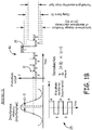
- Figure lA shows photodiode output of a an interferometric fiber optic gyroscope (IFOG) with square-wave modulation during normal operation;
- IFOG interferometric fiber optic gyroscope
- Figure 1B shows operation of a closed loop interferometric fiber optic gyroscope (IFOG) with square-wave modulation during a transient event;
- IFOG interferometric fiber optic gyroscope
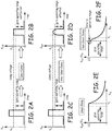
- Figures 2A-2F show exemplary ideal and non-ideal clamping
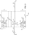
- Figure 3 shows an embodiment of a clamp-point active circuit in accordance with the present invention
- Figure 4A shows a simulated piece-wise linear input waveform
- Figure 4B shows simulated output waveforms responsive to the input waveform of Figure 4A being input to an ideal linear circuit, a prior art clamping circuit, and the circuit of Figure 1 ;
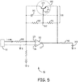
- FIGS. 5 and 6 show embodiments of clamp-point active circuits in accordance with the present invention
- Figure 7 shows simulated output waveforms responsive to an input triangle waveform being input to a prior art clamping circuit and the circuit of Figure 6 ;
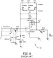
- Figure 8 shows a prior art clamping circuit
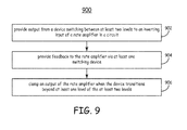
- Figure 9 is a flow diagram representative of a method of extending an operating range and improving a linearity of an output of a circuit in accordance with the present invention.
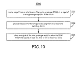
- Figure 10 is a flow diagram representative of a method of extending an operating range and improving a linearity of an output of a circuit receiving input from an interferometric fiber optic gyroscope in accordance with the present invention.
- Embodiments of clamping circuits in a signal processing path are described herein. These clamping circuits allow for use of extended gain in FOG or interferometric fiber optic gyroscope (IFOG) signal processing without distortion of voltage waveforms that are otherwise within the safe operating range of the electronic components. Circuitry is used to clamp input voltages to vulnerable electronic components to a safe operating range (below the voltage damage threshold or other desirable threshold V d ).
- the desirable threshold V d is a maximum safe voltage or a maximum level of the desired operating range.
- An ideal clamping circuit is able to: 1) pass, without distortion, voltages within some selected clamping range V c that is limited to a desired clamp level such that V c ⁇ V d ; and 2) prevent or limit voltage excursions above the voltage damage threshold or other desirable threshold V d to the selected clamping range.
- the selected clamping range is greater than or equal to the normal operating voltage range.
- the normal operating voltage range is also referred to herein as the "normal gyro operating range V gor ".
- V c also referred to herein as a clamp voltage V c or a fixed level V c
- V c the desired clamp level V c
- V c the clamp level of the circuit
- FIG. 1A shows photodiode output of an interferometric fiber optic gyroscope (IFOG) with square-wave modulation during normal operation.
- IFOG interferometric fiber optic gyroscope
- normal operation of an interferometric fiber optic gyroscope is operation of the IFOG when no transient events are being experienced by the IFOG.
- modulation waveform 25 the photodetector output is essentially a square wave, shown as output waveform 30, with very short spikes 31 or glitches 31 at each transition of the square wave.
- photodiode output refers either directly to the photocurrent output of the photodiode or to the voltage output of a transimpedance amplifier which converts photocurrent to voltage.
- the alternating square wave phases are labeled A and B.
- the transition from level A to level B is referred to herein as a "transitioning event” and a “linear transitioning event”.
- the linear transitioning events from level A to level B or from level B to level A are referred to herein as "normal transitions” and do not require clamping.
- the difference signal (A-B) typically obtained by square-wave demodulation, is greater than zero if the gyroscope is rotating (spinning) in one direction and the difference signal (A-B) is less than zero the gyroscope is rotating (spinning) in the other (opposite) direction.
- a ⁇ closed-loop' IFOG circuit nulls out this A-B difference signal by providing phase correction to the light beams. The amount of correction required to null the signal is proportional to the rate that the coil (gyro) is spinning.
- linear A and B signals are critical to obtaining a correct spin rate value. If the response is not linear, there are errors in the performance of the IFOG rate measurement.
- a high-performance IFOG rate amplifier must demonstrate linearity for both the A and the B signals to measure rotation rate accurately.
- the electronics When slewing from the A phase to the B phase of bias modulation, the electronics rapidly moves the operating point over the maximum output of the gyroscope (the peak of the interferogram), and at this point a spike in optical power is generated (e.g., spike 31).
- the square wave of the photodetector waveform 30 is normally of very low amplitude.
- the amplitude is zero for null rotation rate in an open-loop gyroscope or for null acceleration in a closed-loop gyroscope.
- the amplitude of the square wave approaches the desired clamp level V c . In this case, it is important that the clamp circuit not distort the generally square shape of the photodetector waveform 30 for any voltage V ⁇ V c .
- the clamp output be linear in the square wave input voltage (i.e., the square-wave modulation waveform 25), as long as the input voltage is less than or equal to the desired clamp level V c .
- Such clamping linearity is needed to ensure good scale factor linearity of the gyroscope.
- FIG. 1B shows an operation of an interferometric fiber optic gyroscope (IFOG) with a square-wave modulation during a transient event.
- IFOG interferometric fiber optic gyroscope
- a transient event generates a pulse 35 in the photodetector waveform 40 that exceeds the desired clamp level V c and exceeds the saturation damage threshold (V s or V d ) of downstream electronics.
- V s or V d saturation damage threshold
- Transient events from level A to the level C or from level B to level C are generally infrequent events that would, in the absence of clamping, push the signal level beyond the saturation or damage threshold of downstream electronics.
- the transient events are clamped to the selected desired clamp level V c ⁇ V d (e.g., the defined range) by the circuits described herein.
- Figures 2A-2F show exemplary ideal and non-ideal clamping.
- Figures 2A-2B show ideal clamping for V m and V out , respectively.
- An exemplary input voltage pulse V m shown in Figure 2A is clamped as an exemplary output voltage pulse V out shown in Figure 2B to a maximum desired clamp level V c .
- the output voltage pulse V out is flat.
- the voltage of an exemplary gyroscope operating range V gor is shown to be slightly less than the clamp voltage V c .
- any input voltage within the gyroscope operating range V gor is unaffected by the clamping circuit, and the ratio of V out /V in (shown in Figure 2E ) is constant and equal to unity (1.0) throughout the gyroscope operating range V gor and up to the clamp voltage V c .
- FIGS 2C-2D show non-ideal clamping.
- the exemplary input voltage pulse V m shown in Figure 2C is clamped as a non-ideal exemplary output voltage pulse V out ( Figure 2D ) with distortion at voltages less than or equal to the clamp voltage V c .
- the exemplary output voltage pulse V out is a poor representation of V m because of the non-ideal clamping.
- portions of the output voltage V out differ from V in even where V m is within the gyroscope operating range V gor .
- the ratio of V out /N in is less than one (1) within the gyroscope operating range V gor .
- the gyroscope signal is corrupted when the ratio of V out /N in is less than one (1) within the gyroscope operating range V gor .
- Transient events mandate the need for a clamping circuit.
- An overshoot spike may periodically occur in fiber optic gyroscopes due to dead band suppression in which randomizing modulation schemes are used.
- Randomizing modulation schemes generate a photodetector waveform that is periodically modulated with a square pulse (typically on the order of microseconds in duration) of random amplitude and direction. With high gain in the signal processing electronics, such pulses may be amplified well above the voltage saturation or damage thresholds V s or V d .
- a clamping circuit is needed to prevent damage or saturation.
- transient events are radiation events and mechanical shock.
- the photodetector is briefly flooded with photocurrent, potentially creating a voltage spike above the upper limit of the voltage saturation or damage thresholds V s or V d .
- mechanical shock may create a rapid optical loss transient, driving the voltage near a lower voltage saturation or damage threshold V s or V d .
- These transient events cause a fast temporary decrease or increase in optical power, and typically reduce the rate measurement accuracy of an IFOG.
- the large optical transitions or glitches that reduce rate measurement accuracy of the IFOG are referred to herein as "large gyroscope rate events".
- the embodiments of circuits described herein increase linearity in the normal operating range and reduce harmonic distortion during the clamping process.
- the gyroscope firmware may be configured to reject the glitches or spikes by skipping acquisition samples during the transition event. However, distortion created by the clamping circuitry may allow glitch noise to extend beyond the transition event and corrupt the gyroscope signal.
- the circuits described herein are applicable to applications that require a linear output from an amplifier, which receives signals from a device transitioning between two or more levels.
- the circuits described herein create a linear operating range (i.e., a low differential gain error) over an extended dynamic range and reduce the probability of the rate amplifier going non-linear at the extremity of operating range.
- the circuits described herein use an active switching device, such as, a bipolar-junction transistor (BJT), to provide an improved linear transfer function up to a desired clamping level (i.e., clamping function).
- BJT bipolar-junction transistor
- the circuits described herein are designed to include the desired operating range as required or desired by a user of the circuit.
- an "improved linear transfer function" output from the circuit is an improvement of the transfer function output from a prior art clamping circuit.
- FIG. 3 shows an embodiment of a clamp-point active circuit 10 in accordance with the present invention.
- the clamp-point active circuit 10 is also referred to herein as circuit 10.
- Circuit 10 includes a rate amplifier 100, a PNP bipolar junction transistor 200 (also referred to herein as “active switching device 200" and “switching device 200"), an NPN bipolar junction transistor 201(also referred to herein as “active switching device 201” or “switching device 201”), a positive voltage source 210, a first diode 220, a second diode 221, a negative voltage source 211, a third diode 230, and a fourth diode 231.
- the inverting input 105 of the rate amplifier 100 receives pulses via an input resistor 252 from a device 50.
- the non-inverting input 106 of the rate amplifier 100 is connected to a grounded line.
- An output resistor 255 and an output capacitor 256 are arranged in series to receive output signals from the output 107 of the rate amplifier 100.
- the output signals are provided to back end gyroscope processing circuits (not shown) as required by the type of technical application provided by the device 50.
- the rate amplifier 100 receives output from the device 50 that is switching between two levels.
- the device 50 is a rate photodetector of an interferometric fiber optic gyroscope.
- the rate amplifier 100 is a rate gyroscope amplifier 100. Therefore, the terms "rate amplifier” and "rate gyroscope amplifier” are used interchangeably herein.
- the PNP bipolar-junction transistor 200 and the NPN bipolar junction transistor 201 are in respective feedback loops of the rate gyroscope amplifier 100. PNP bipolar-junction transistor 200 and the NPN bipolar junction transistor 201 receive an output from the rate gyroscope amplifier 100.
- the bipolar-junction transistor switching action in the circuit 10 causes the rate gyroscope amplifier 100 to output signals having a transfer function within the desired operating range that is more linear than signals output from an amplifier in a prior art clamping circuit, which does not include the bipolar-junction transistor switching action of the circuit 10.
- An exemplary prior art clamping circuit is shown in Figure 8 .
- Circuit 10 uses the two bipolar junction transistors 200 and 201 and four diodes 220, 221, 230, and 231 in a symmetrical fashion.
- the PNP bipolar junction transistor 200, the first diode 220, and the second diode 221 form a first-half circuit 21.
- the PNP bipolar junction transistor 200 provides a low-impedance feedback path from the output 107 of the rate gyroscope amplifier 100 to the inverting input 105 of the rate gyroscope amplifier 100 when the output 107 of the rate gyroscope amplifier 100 exceeds a preselected voltage.
- the preselected voltage is 1 V + V BE (about +1.6V), where V BE is the base-emitter voltage of the transistor.
- First diode 220 (also referred to herein as PN diode 220) protects the PNP bipolar junction transistor 200 base-emitter junction from damaging reverse-voltage breakdown.
- Second diode 221 (also referred to herein as Schottky diode 221) prevents collector/emitter (CE) saturation of the PNP bipolar junction transistor 200 and improves operating speed.
- the NPN bipolar junction transistor 201 provides a low-impedance feedback path from the output 107 of the rate gyroscope amplifier 100 to the inverting input 105 of the rate gyroscope amplifier 100 when the output of the rate gyroscope amplifier 100 drops below the negative of the preselected value.
- the negative of the preselected voltage is -1V - V BE (about -1.6V).
- Fourth diode 231 protects the NPN bipolar junction transistor 201 base-emitter junction from damaging reverse-voltage breakdown.
- the third diode prevents collector/emitter (CE) saturation of the NPN bipolar junction transistor 201 and improves operating speed.
- the first-half circuit 21 and the second-half circuit 22 together provide high linearity in the operating range, a maximum operating range, and rapid clamping beyond the operating range.
- An output of the positive voltage source 210, an anode 225 of the first diode 220, and a cathode 227 of the second diode 221 are connected to a base 272 of the PNP bipolar junction transistor 200.
- a connection between two circuit elements is either a direct connection between the elements or a connection between the elements made via another circuit element (for example, a resistor or an inductor). In one implementation of this embodiment, the connections are trace lines on a circuit board.
- a collector 270 of the PNP bipolar junction transistor 200 is connected to the inverting input 105 of the rate gyroscope amplifier 100.
- An anode 228 of the second diode 221 is connected to the collector 270 of the PNP bipolar junction transistor 200 and to the inverting input 105 of the rate gyroscope amplifier 100.
- a cathode 226 of the first diode 220 is connected to the output 107 of the rate gyroscope amplifier 100 through resistor 254 and is also connected to the emitter 271 of the PNP bipolar junction transistor 200.
- the emitter 271 of the PNP bipolar junction transistor 200 is connected to the output 107 of the rate gyroscope amplifier 100 through resistor 254.
- An output of the negative voltage source 211, an anode 235 of the third diode 230, and a cathode 237 of the fourth diode 231 are connected to a base 282 of the NPN bipolar junction transistor 201.
- a collector 280 of the NPN bipolar junction transistor 201 is connected to the inverting input 105 of the rate gyroscope amplifier 100.
- a cathode 236 of the third diode 230 is connected to the collector 280 of the NPN bipolar junction transistor 201 and to the inverting input 105 of the rate gyroscope amplifier 100.
- An anode 238 of the fourth diode 231 is connected to the output 107 of the rate gyroscope amplifier 100 through resistor 253 and is also connected to the emitter 281 of the NPN bipolar junction transistor 201.
- the emitter 281 of the NPN bipolar junction transistor 201 is connected to the output 107 of the rate gyroscope amplifier 100 through resistor 253.
- a feedback resistor 251 and a feedback capacitor 250 are configured in parallel to the rate gyroscope amplifier 100.
- the feedback resistor 251 and feedback capacitor 250 are connected from the output 107 of the rate gyroscope amplifier 100 to the inverting input 105 of the rate gyroscope amplifier 100. In this manner, feedback is provided to the rate gyroscope amplifier 100.
- the clamping range of the clamp-point active circuit 10 is easily adjusted by replacing the precision voltage sources 210 and 211 with precision voltage sources 210 and 211 of different values.
- the precision voltage sources 210 and 211 are tunable voltage sources and the clamping range of the clamp-point active circuit 10 is adjusted by tuning the precision voltage sources 210 and 211.
- the switching of the switching devices 200 and 201 extends the linear operating range of circuit 10 and simultaneously ensures greatest probability of clamping transient events that could otherwise exceed the operating range.
- the switching of the switching devices 200 and 201 in circuit 10 of Figure 3 causes the rate amplifier 100 to amplify with high linearity in a desired operating range and to clamp the transient events received from the transitioning device 50 that are outside the desired operating range (e.g., greater than V d ) to a fixed level V c .
- the rate amplifier 100 is clamped when the device 50 transitions beyond at least one level (e.g., beyond level B to level C of Figure 1B ) of the at least two levels.
- Circuit 10 is designed with selected elements to maximize the percent of clamped transient events over the extended operating range.
- the percentage of clamped transient events is increased (improved) to 99.99 %. In another implementation of this embodiment, the percentage of clamped transient events is increased to 99.99 %. In yet another implementation, the percentage of clamped transient events is increased to 99.999 %. Circuit 10 is designed with selected elements to ensure the desired percentage of clamped transient events over the extended operating range. In yet another implementation of this embodiment, the percentage of clamped transient events is maximized over the extended operating range.
- the first diode 220 is diode 1N4148
- the second diode 221 is diode 1N5711
- the PNP bipolar junction transistor 200 is a transistor 2N2907A
- the third diode 230 is diode 1N5711
- the fourth diode 231 is diode 1N4148
- the NPN bipolar junction transistor 201 is transistor 2N2222A.
- the feedback resistor 251 is a 6000 ohm resistor
- the feedback capacitor 250 is a 4 pF capacitor
- resistor 254 is a 200 ohm resistor
- the resistor 253 is a 200 ohm resistor.
- the input resistor 252 is a 2000 ohm resistor
- the output resistor 255 is an 84.5 ohm resistor
- the output capacitor 256 is a 1 pF capacitor.
- the circuit 10 includes other diodes and transistors and other values for the resistors and capacitors.
- Figure 4A shows a simulated piece-wise linear input waveform 50.
- Figure 4B shows simulated output waveforms 60, 70, and 80 responsive to the input waveform 50 of Figure 4A being input to an ideal linear circuit, a prior art clamping circuit, and the circuit 10 of Figure 1 , respectively.
- the output waveform 60 in Figure 4B shows the pure linear output (for comparison before the breakpoint).
- the output waveform 70 which is superimposed on the output waveform 60, shows the output from an exemplary non-ideal prior art clamping circuit (see Figure 8 ) that lacks the bipolar-junction transistor switching action in the circuit.
- the output waveform 80 which is superimposed on the output waveforms 60 and 70, shows the output from the circuit 10 ( Figure 3 ), which is more linear than the output waveform 70 from the prior art circuit. Since the output waveform 80 is more linear than the prior art output waveform 70, the operating range of the output waveform 80 is extended beyond the operating range of the prior art output waveform 70. Ideally, the output waveform 80 has an ideal slew rate near 3 volts/microsecond before the break-point. This operation supports IFOG A-B integration for accurate rate determination at rates scaled below the break-point, by design. Thus, circuit 10 of Figure 3 provides a clamp-point that clamps higher than a prior art clamping circuit and reduces distortion for the statistical ensemble of gyroscope optical transition events.
- An acceptably linear function is a function that varies from the ideal by less than some defined threshold, possibly 100 parts per million (ppm); in other words, the circuit is highly linear if V out /N in equals 1.0 to within 100 ppm.
- a highly linear function is a function that varies from the ideal by less than 10 ppm.
- the region where clamping occurs is considered to be highly linear when the region in which clamping occurs includes oscillations (ringing) of less than 1% of the clamp voltage V c for less than 5% of the initial time of the whole time that the clamping occurs.
- the region where clamping occurs is considered to be highly linear when the region in which clamping occurs includes oscillations (ringing) of less than 3% of the clamp voltage V c for less than 10% of the initial time of the whole time that the clamping occurs.
- the transfer function is highly linear when the region where clamping occurs includes oscillations (ringing) of less than 1% of the clamp voltage V c rather than ringing of 10% of the clamp voltage V c available from a prior art clamping circuit.
- the linearity of the transfer function is improved so that ringing occurs for less than 5% the whole time that the clamping occurs rather than the ringing in a prior art clamping circuit that occurs for 20% of the whole time that the clamping occurs.
- clamping circuits do not require voltages or networks that are external to the rate feedback network. These embodiments may reduce random and systematic noise levels over circuits that require external sources/circuits, since voltages or networks (including circuit elements) external to the rate feedback network can introduce extra noise to the circuit.
- the embodiments of clamping circuits that do not require voltages or networks external to the rate feedback network circuits are significantly faster at engaging/disengaging the clamping function than prior art clamping circuits.
- Such circuits produce scale factor linearity performance that is better than the prior art clamping circuits over temperature or other environmental variations.
- An ideal rate amplifier behaves linearly over amplitude and temperature, and clamps but does not saturate under the operating conditions described.
- FIG. 5 shows an embodiment of a clamp-point active circuit 11 in accordance with the present invention.
- the clamp-point active circuit 11 is also referred to herein as circuit 11.
- Circuit 11 includes rate amplifier 101, a PNP bipolar junction transistor 300 (also referred to herein as “active switching device 300" and “switching device 300"), a first resistor 310, a second resistor 311, and a feedback capacitor 341.
- the rate amplifier 101, the PNP bipolar junction transistor 300, the first resistor 310, and the second resistor 311 together form a rate feedback network 85 to the rate gyroscope amplifier 101.
- the circuit 11 also includes an input resistor 350, an output resistor 342, and an output capacitor 343.
- the inverting input 115 of the rate amplifier 101 receives current via the input resistor 350.
- the non-inverting input 116 of the rate amplifier 101 is grounded.
- the rate amplifier 101 receives output from a device 50 that is switching between two levels.
- the device 50 is a rate photodetector of an interferometric fiber optic gyroscope.
- the rate amplifier 101 is a rate gyroscope amplifier 101.
- the PNP bipolar-junction transistor 300 is in a feedback loop of the rate gyroscope amplifier 101.
- PNP bipolar-junction transistor 300 receives an output from the rate gyroscope amplifier 101.
- a bipolar-junction transistor switching action in the circuit 11 gives the rate gyroscope amplifier 101 a transfer function with improved linearity in the normal operating voltage range and improved clamping above this range.
- An emitter 371 of the PNP bipolar junction transistor 300 is connected to the output 117 of the rate gyroscope amplifier 101.
- a collector 370 of the PNP bipolar junction transistor 300 is connected to the inverting input 115 of the rate gyroscope amplifier 101.
- a base 372 of the PNP bipolar junction transistor 300 is connected to a node 312 between the first resistor 310 and the second resistor 311 in series with each other.
- the first resistor 310 and the second resistor 311 are in parallel to inverting input 115 and the output 117 of the rate gyroscope amplifier 101.
- the feedback capacitor 341 is also in parallel to the inverting input 115 and the output 117 of the rate gyroscope amplifier 101.
- the clamping range of the clamp-point active circuit 11 is easily adjusted by replacing the resistor 311 with a resistor 311 of another value.
- the PNP bipolar junction transistor 300 is a MM3906 transistor
- the feedback resistor 310 is a 3,650 ohm resistor
- the feedback resistor 311 is a 665 ohm resistor
- the feedback capacitor 341 is an 18 pF capacitor
- resistor 342 is a 169 ohm resistor
- the resistor 350 is a 383 ohm resistor.
- the circuit 11 includes another transistor and other values for the resistors and capacitors.
- the switching of the switching device 300 in circuit 11 of Figure 5 extends the linear operating range of circuit 11 and simultaneously ensures greatest probability of clamping transient events that could otherwise exceed the operating range.
- the switching of the switching device 300 causes the rate amplifier 101 to amplify with high linearity in a desired operating range and to clamp transient events received from the transitioning device 50 that are outside the desired operating range to a fixed level (clamp voltage) V c .
- the rate amplifier 101 is clamped when the device 50 transitions beyond at least one level (e.g., beyond level B to level C of Figure 1B ) of the at least two levels A and B ( Figure 1B ).
- Circuit 11 is designed with selected elements to maximize the percent of clamped transient events over the extended operating range.
- FIG. 6 shows an embodiment of a clamp-point active circuit 12 in accordance with the present invention.
- the clamp-point active circuit 12 is also referred to herein as “circuit 12" and “cascode circuit 12".
- Circuit 12 includes a rate amplifier 102, a PNP bipolar junction transistor 400 (also referred to herein as “active switching device 400” and “switching device 400"), an NPN bipolar junction transistor 401 (also referred to herein as “active switching device 401” and “switching device 401”), a first resistor 320, a second resistor 321, a feedback capacitor 340, a resistor 323, and a resistor 322.
- the rate amplifier 102, the PNP bipolar junction transistor 400, the NPN bipolar junction transistor 401, the first resistor 320, the second resistor 321, the feedback capacitor 340, and the resistors 323 and 322 together form a rate feedback network 86 to the rate gyroscope amplifier 102.
- Circuit 12 also includes an input resistor 351, an output resistor 344, and an output capacitor 345.
- the inverting input 125 of the rate amplifier 102 receives current through the input resistor 351.
- the non-inverting input 126 of the rate amplifier 102 is connected to a grounded line.
- the rate amplifier 102 receives output from a device 50 that is switching between at least two levels (e.g., levels A and B).
- the device 50 is a rate photodetector of an interferometric fiber optic gyroscope and the rate amplifier 102 is a rate gyroscope amplifier 102.
- the PNP bipolar-junction transistor 400 and the NPN bipolar junction transistor 401 are in a feedback loop of the rate gyroscope amplifier 102.
- a bipolar-junction transistor switching action in the circuit 12 causes the rate gyroscope amplifier 102 to output an improved transfer function.
- An emitter 461 of the PNP bipolar junction transistor 400 is connected to the output 127 of the rate gyroscope amplifier 102.
- a collector 460 of the PNP bipolar junction transistor 400 is connected to an inverting input 125 of the rate gyroscope amplifier 102 through a resistor 323.
- a base 462 of the PNP bipolar junction transistor 400 is connected to a node 412 between a first resistor 320 and a second resistor 321 in series with each other.
- the first resistor 320 and the second resistor 321 are in parallel to the inverting input 125 and the output 127 of the rate gyroscope amplifier 102.
- a feedback capacitor 340 is also in parallel to the inverting input 125 and the output 127 of the rate gyroscope amplifier 102.
- An emitter 471 of the NPN bipolar junction transistor 401 is connected via a resistor 322 to the inverting input 125 of the rate gyroscope amplifier 102.
- a collector 470 of the NPN bipolar junction transistor 401 is connected to the output 127 of the rate gyroscope amplifier 102.
- a base 472 of the NPN bipolar junction transistor 401 is connected via the resistor 323 to the inverting input 125 of the rate gyroscope amplifier 102.
- the base 472 is also connected to the collector 460 of the PNP bipolar junction transistor 400.
- the clamping range of the clamp-point active circuit 11 is easily adjusted by replacing the resistor 321 with a resistor 321 of another value.
- Circuit 12 is a cascode circuit 12 which permits fast, highly linear response.
- the circuits 11 or 12 are independent of voltages external to the rate feedback network 85 or 86, respectively, and thus independent of the extra noise generated by external voltages.
- the PNP bipolar junction transistor 400 is a transistor MM3906
- the NPN bipolar junction transistor 401 is a transistor MPS2222
- the feedback resistor 320 is a 3711 ohm resistor
- the feedback resistor 321 is a 604 ohm resistor
- the feedback capacitor 340 is a 7 pF capacitor
- resistor 323 is a 10K ohm resistor
- the resistor 322 is a 1 ohm resistor.
- the input resistor 351 is a 383 ohm resistor and the output resistor 344 is a 169 ohm resistor.
- the circuit 12 includes other transistors and other values for the resistors and capacitors.
- the switching of the switching devices 400 and 401 in circuit 12 of Figure 6 extends the linear operating range of circuit 12 and simultaneously ensures greatest probability of clamping transient events that could otherwise exceed the operating range.
- the switching of the switching devices 400 and 401 causes the rate amplifier 102 to amplify with high linearity in the desired operating range and to clamp transient events received from the transitioning device 50 that are outside the desired operating range to a fixed level (clamp voltage) V c .
- the rate amplifier 102 is clamped when the device 50 transitions beyond at least one level (e.g., beyond level B to level C of Figure 1B ) of the at least two levels A and B ( Figure 1B ).
- Circuit 12 is designed with selected elements to maximize the percent of clamped transient events over the extended operating range.
- Figure 7 shows simulated output waveforms 170 and 180 responsive to an input triangle waveform 150 being input to a prior art clamping circuit 13, and the circuit 12 of Figure 6 .
- Figure 8 shows a prior art clamping circuit 13.
- the input waveform 150 in Figure 7 shows the pure linear input.
- the triangle waveform 151 is the DC offset difference removed from the output waveform 150 by offset circuitry at the inverting input node 125 of the rate amplifier 102 of circuit 12 ( Figure 6 ).
- the output waveform 170 shows the output from an exemplary non-ideal prior art clamping circuit 13 ( Figure 9 ) that lacks the bipolar-junction transistor switching action in the circuit.
- the output waveform 180 shows the output from the cascode circuit 12 ( Figure 6 ).
- circuit 11 is better than that of the prior art clamping circuit 13 ( Figure 8 ), but that is less than that of cascode circuit 12.
- Circuit 11 advantageously requires fewer components to provide high linearity.
- the linearity and distortion performance of circuit 12 is very high, however circuit 12 requires more than twice the components required in circuit 11.
- the bipolar-junction transistor switching action clamps the output of the rate gyroscope amplifiers 100, 101, and 102 in the circuits 10, 11, and 12, respectively, to the desired clamp level V c ⁇ V d while providing a transfer function that is more linear in the normal operating voltage range V gor .
- the bipolar-junction transistor switching action in the circuits 10, 11, and 12 causes the rate gyroscope amplifiers 100, 101, and 102, respectively, to output signals below the desired clamp level V c with a transfer function that is more linear than signals output from an amplifier without the bipolar-junction transistor switching action of the circuits 10, 11, or 12.
- the circuits described herein include additional elements in series and/or in parallel with the described elements.
- circuits 10, 11 and 12 shown herein Based on the applied bias modulation amplitude (modulation depth) of different gyroscopes, different embodiments of the circuits 10, 11 and 12 shown herein will be preferred.
- the circuits 11 and 12 of Figures 5 and 6 are the better circuits for gyroscopes having 3 ⁇ 4 ⁇ modulation
- the circuit 10 of Figure 3 is a better circuit for gyroscopes having ⁇ /2 modulation.
- Figure 9 is a flow diagram representative of a method 900 of extending an operating range and improving a linearity of an output of a circuit in accordance with the present invention.
- the circuit described with reference to method 900 is either circuit 10, 11 or 12.
- output from a device 50 switching between at least two levels is received at an inverting input of a rate amplifier 100, 101 or 102 in the circuit 10, 11 or 12, respectively.
- the switching device is least one PNP bipolar junction transistor.
- the feedback is provided to the rate amplifier 100 via bipolar junction transistors 200 and 201.
- the feedback is provided to the rate amplifier 101 via the PNP bipolar junction transistor 300.
- the feedback is provided to the rate amplifier 102 via the PNP bipolar junction transistor 400 and NPN bipolar junction transistor 401.
- an output of the rate amplifier is clamped when the device transitions beyond at least one level of the at least two levels while simultaneously the linear operating range of the circuit is extended.
- the rate amplifiers 100, 101, and 102 in the circuits 10, 11, and 12, respectively are clamped when the device transitions from level A to a level beyond level B, such as level C.
- a percentage of linear transitioning events e.g., transitioning events that fall below the desired clamp level V c ⁇ V d , either with or without clamping as needed
- a percentage of clamped transient events e.g., transient events that are clamped to the desired clamp level V c ⁇ V d
- a linear transitioning event is a transitioning event that results in a highly linear transfer function from the rate amplifier.
- the linear transitioning events provide reduced distortion of voltage waveforms that are otherwise within the safe operating range of the electronic components.
- Figure 10 is a flow diagram representative of a method 1000 of extending an operating range and improving a linearity of an output of a circuit receiving input from an interferometric fiber optic gyroscope (IFOG) in accordance with the present invention.
- the circuit described with reference to method 1000 is either circuit 10, 11 or 12.
- output from an IFOG 50 transitioning between two levels is received at an input of a rate gyroscope amplifier 100, 101 or 102 in the circuit 10, 11 or 12, respectively.
- the switching device is least one PNP bipolar junction transistor.
- the feedback is provided to the rate amplifier 100 via bipolar junction transistors 200 and 201 by: connecting a collector 270 of the PNP bipolar junction transistor 200 to the inverting input 105 of the rate amplifier 100; connecting a collector 280 of the NPN bipolar junction transistor 201 to the inverting input 105 of the rate amplifier 100; connecting an output of a positive voltage source 210, an anode 225 of the first diode 220, and the cathode 227 of the second diode 221 to the base 272 of the PNP bipolar junction transistor 200; and connecting an output of the negative voltage source 211, the anode 235 of the third diode 230, and the cathode 237 of the fourth diode 231 to the base 282 of the NPN bipolar junction
- the feedback is provided to the rate amplifier 101 via the PNP bipolar junction transistor 300 by: connecting the output 117 of the rate amplifier 101 to the emitter 371 of the PNP bipolar junction transistor 300; connecting the collector 370 of the PNP bipolar junction transistor 300 to the inverting input 115 of the rate amplifier 101; and connecting the base 372 of the PNP bipolar junction transistor 300 to a node 312 between the first resistor 310 and the second resistor 311 that are in series with each other.
- the feedback is provided to the rate amplifier 102 via the PNP bipolar junction transistor 400 and NPN bipolar junction transistor 401 by: connecting the output 127 of the rate amplifier 102 to the emitter 461 of the PNP bipolar junction transistor 400; connecting the collector 460 of the PNP bipolar junction transistor 400 to the inverting input 125 of the rate amplifier 102 via a resistor 323; and connecting the base 462 of the PNP bipolar junction transistor 400 to a node 412 between the first resistor 320 and the second resistor 321 that are in series with each other; connecting the collector 460 of the PNP bipolar junction transistor 400 to a base 472 of an NPN bipolar junction transistor 401; connecting the collector 470 of the NPN bipolar junction transistor 401 to the output 127 of the rate amplifier 102; and connecting the emitter 471 of the NPN bipolar junction transistor 400 to the input 125 of the rate amplifier 102 via a third resistor 322.
- an output of the rate gyroscope amplifier 100, 101 or 102 is clamped when the IFOG 50 transitions beyond at least one level of the at least two levels.
- the rate gyroscope amplifiers 100, 101, and 102 in the circuits 10, 11, and 12, respectively are clamped to a desired clamp level V c when the IFOG 50 transitions from level A to a level beyond level B, such as level C.
- a percentage of linear transitioning events e.g., transitioning events that fall below the desired clamp level V c ⁇ V d , either with or without clamping as needed is increased over an extended operating range.
- the percentage of clamped transient events (e.g., transient events that are clamped to the desired clamp level V c ⁇ V d ) is increased for an extended operating range.
- the precision voltage sources 210 and 211 are switched out to provide the clamp adjustment.
- the precision voltage sources 210 and 211 are tunable, and the precision voltage sources 210 and 211 are tuned to provide the clamp adjustment.
- the resistors 311 or 321 are replaced by resistors of different resistance values in order to provide an adjustment for clamp action voltage.
- the resistors 311 or 321 are tunable and the resistance value is tuned in order to provide an adjustment for clamp action voltage. In this manner, for a plurality of transitioning events, the percentage of clamped transient events is increased for an extended operating range.
Landscapes
- Engineering & Computer Science (AREA)
- Power Engineering (AREA)
- Physics & Mathematics (AREA)
- General Physics & Mathematics (AREA)
- Radar, Positioning & Navigation (AREA)
- Electromagnetism (AREA)
- Optics & Photonics (AREA)
- Remote Sensing (AREA)
- Spectroscopy & Molecular Physics (AREA)
- Nonlinear Science (AREA)
- Gyroscopes (AREA)
- Amplifiers (AREA)
- Tone Control, Compression And Expansion, Limiting Amplitude (AREA)
Applications Claiming Priority (1)
| Application Number | Priority Date | Filing Date | Title |
|---|---|---|---|
| US13/043,115 US8680911B2 (en) | 2011-03-08 | 2011-03-08 | High-linearity signal-processing amplifier |
Publications (3)
| Publication Number | Publication Date |
|---|---|
| EP2498052A2 true EP2498052A2 (de) | 2012-09-12 |
| EP2498052A3 EP2498052A3 (de) | 2014-08-06 |
| EP2498052B1 EP2498052B1 (de) | 2018-06-13 |
Family
ID=45855489
Family Applications (1)
| Application Number | Title | Priority Date | Filing Date |
|---|---|---|---|
| EP12157997.3A Active EP2498052B1 (de) | 2011-03-08 | 2012-03-02 | Hochlinearer Signalverarbeitungsverstärker |
Country Status (3)
| Country | Link |
|---|---|
| US (1) | US8680911B2 (de) |
| EP (1) | EP2498052B1 (de) |
| JP (1) | JP5932403B2 (de) |
Families Citing this family (6)
| Publication number | Priority date | Publication date | Assignee | Title |
|---|---|---|---|---|
| WO2019022416A1 (ko) * | 2017-07-28 | 2019-01-31 | 주식회사 아모센스 | 전자식 계량기 |
| JP2019054438A (ja) * | 2017-09-15 | 2019-04-04 | アズビル株式会社 | 光電センサ |
| JP2020195103A (ja) * | 2019-05-30 | 2020-12-03 | 株式会社日立製作所 | 増幅回路 |
| CN113739783B (zh) * | 2021-11-08 | 2022-03-01 | 华中光电技术研究所(中国船舶重工集团公司第七一七研究所) | 一种光纤陀螺振铃效应误差抑制系统及抑制方法 |
| CN115833764A (zh) * | 2021-12-01 | 2023-03-21 | 深圳市速腾聚创科技有限公司 | 前端放大电路及光电系统 |
| CN121261656A (zh) * | 2025-12-03 | 2026-01-02 | 四川升华电源科技有限公司 | 负反馈补偿电路 |
Family Cites Families (25)
| Publication number | Priority date | Publication date | Assignee | Title |
|---|---|---|---|---|
| US3497830A (en) * | 1968-03-20 | 1970-02-24 | Bell Telephone Labor Inc | Gated operational amplifier |
| US3648071A (en) * | 1970-02-04 | 1972-03-07 | Nat Semiconductor Corp | High-speed mos sense amplifier |
| DE2748647C2 (de) * | 1977-10-29 | 1986-06-19 | Ernst Leitz Wetzlar Gmbh, 6330 Wetzlar | Verstärker für elektrische Signale |
| JPS579114A (en) * | 1980-06-20 | 1982-01-18 | Fujitsu Ltd | Limiter circuit |
| JPS5767305A (en) * | 1980-10-15 | 1982-04-23 | Hitachi Denshi Ltd | Limiter circuit |
| FR2498859A1 (fr) * | 1981-01-23 | 1982-07-30 | Thomson Csf | Dispositif de limitation du signal de luminance et emetteur de television comportant un tel dispositif |
| JPH0546092Y2 (de) * | 1987-03-25 | 1993-12-01 | ||
| US5028889A (en) | 1989-08-25 | 1991-07-02 | Orest Fedan | Oscillator having a limiter composed of a symmetric active clamp |
| GB2250885B (en) * | 1990-12-13 | 1994-07-20 | Motorola Inc | Clamp circuit |
| JPH0629755A (ja) * | 1992-07-10 | 1994-02-04 | Mitsubishi Electric Corp | 前置増幅器 |
| US5381106A (en) * | 1992-10-28 | 1995-01-10 | Samsung Electronics Co., Ltd. | Clipper circuitry suitable for signals with fractional-volt amplitudes |
| US5521555A (en) * | 1994-07-25 | 1996-05-28 | Litton Systems, Inc. | Ultra low noise optical receiver |
| US5793241A (en) * | 1995-11-30 | 1998-08-11 | Cherry Semiconductor Corporation | High speed active op-amp clamp |
| US5856760A (en) | 1996-11-07 | 1999-01-05 | Raytheon Company | Overdrive protection clamp scheme for feedback amplifiers |
| JP3786556B2 (ja) * | 2000-02-23 | 2006-06-14 | シャープ株式会社 | 受光アンプ回路 |
| US6621321B2 (en) * | 2001-06-20 | 2003-09-16 | Analog Devices, Inc. | Circuit for conditioning output waveform |
| US20030090326A1 (en) * | 2001-11-14 | 2003-05-15 | Victor Pogrebinsky | Transimpedance amplifier with dual gain outputs |
| US6744519B2 (en) | 2002-04-30 | 2004-06-01 | Honeywell International Inc. | Methods and apparatus for fiber optic gyroscope dead band error suppression modulation |
| JP3864864B2 (ja) * | 2002-07-11 | 2007-01-10 | 株式会社デンソー | クランプ回路 |
| US6864751B1 (en) * | 2003-09-08 | 2005-03-08 | Texas Instruments Deutschland Gmbh | Transimpedance amplifier with adjustable output amplitude and wide input dynamic-range |
| JP3894925B2 (ja) * | 2004-03-19 | 2007-03-22 | 日本航空電子工業株式会社 | クローズドループ方式光ファイバジャイロ |
| JP4539395B2 (ja) * | 2005-03-25 | 2010-09-08 | ヤマハ株式会社 | パワーアンプ |
| JP2007028372A (ja) * | 2005-07-20 | 2007-02-01 | Matsushita Electric Ind Co Ltd | 受光増幅回路およびそれを用いた光ピックアップ装置 |
| US7489199B2 (en) | 2006-06-15 | 2009-02-10 | Thomas Szepesi | Saturation detector and warning circuit including clamp |
| US7817284B2 (en) * | 2007-08-08 | 2010-10-19 | The Charles Stark Draper Laboratory, Inc. | Interferometric fiber optic gyroscope with off-frequency modulation signals |
-
2011
- 2011-03-08 US US13/043,115 patent/US8680911B2/en active Active
-
2012
- 2012-03-02 EP EP12157997.3A patent/EP2498052B1/de active Active
- 2012-03-07 JP JP2012050230A patent/JP5932403B2/ja not_active Expired - Fee Related
Non-Patent Citations (1)
| Title |
|---|
| None |
Also Published As
| Publication number | Publication date |
|---|---|
| JP5932403B2 (ja) | 2016-06-08 |
| US8680911B2 (en) | 2014-03-25 |
| JP2012191616A (ja) | 2012-10-04 |
| EP2498052B1 (de) | 2018-06-13 |
| EP2498052A3 (de) | 2014-08-06 |
| US20120229811A1 (en) | 2012-09-13 |
Similar Documents
| Publication | Publication Date | Title |
|---|---|---|
| EP2498052B1 (de) | Hochlinearer Signalverarbeitungsverstärker | |
| US7652464B2 (en) | RF power sensor with chopping amplifier | |
| US11394349B2 (en) | Transimpedance amplifier | |
| JP6703030B2 (ja) | 高速オーバードライブ回復機能付きトランスインピーダンス増幅器 | |
| JPWO2016047149A1 (ja) | ホール起電力信号検出回路及び電流センサ | |
| US6583882B2 (en) | Apparatus and method using digitally controlled integration for signal detection with improved noise characteristics | |
| US7825735B1 (en) | Dual-range linearized transimpedance amplifier system | |
| US8742314B2 (en) | Light amount detecting apparatus, and light amount information processing apparatus | |
| CN100559704C (zh) | 光接收用前置放大器 | |
| US5498993A (en) | Pulse light-receiving circuit with means to minimize power source noise | |
| US20110089989A1 (en) | Limiter circuit | |
| CN112332791B (zh) | 一种可变增益放大器 | |
| JP2003168933A (ja) | 光受信回路 | |
| US6566955B1 (en) | High bandwidth transresistance amplifier | |
| US7521998B2 (en) | Operational amplifier and scanning electron microscope using the same | |
| US11121686B2 (en) | Amplifier circuit | |
| EP0420128B1 (de) | Detektorschaltung für amplitudenmodulierte Signale | |
| US10211846B1 (en) | Techniques for amplifier output voltage limiting | |
| JP2017169156A (ja) | トランスインピーダンスアンプおよび光信号受信装置 | |
| CN106342289B (zh) | 雪崩光电二极管偏压控制电路 | |
| US8547141B2 (en) | Wide dynamic range, wide bandwidth, voltage to current converter | |
| EP3439175B1 (de) | Eingangsstromanpassung für komplett differentielle transimpedanzverstärker | |
| JP2018078415A (ja) | 光受信回路 | |
| JPH06120747A (ja) | 差動増幅器 | |
| CN117665363A (zh) | 一种基于皮安级对数放大模块的微电流检测系统 |
Legal Events
| Date | Code | Title | Description |
|---|---|---|---|
| PUAI | Public reference made under article 153(3) epc to a published international application that has entered the european phase |
Free format text: ORIGINAL CODE: 0009012 |
|
| 17P | Request for examination filed |
Effective date: 20120302 |
|
| AK | Designated contracting states |
Kind code of ref document: A2 Designated state(s): AL AT BE BG CH CY CZ DE DK EE ES FI FR GB GR HR HU IE IS IT LI LT LU LV MC MK MT NL NO PL PT RO RS SE SI SK SM TR |
|
| AX | Request for extension of the european patent |
Extension state: BA ME |
|
| PUAL | Search report despatched |
Free format text: ORIGINAL CODE: 0009013 |
|
| AK | Designated contracting states |
Kind code of ref document: A3 Designated state(s): AL AT BE BG CH CY CZ DE DK EE ES FI FR GB GR HR HU IE IS IT LI LT LU LV MC MK MT NL NO PL PT RO RS SE SI SK SM TR |
|
| AX | Request for extension of the european patent |
Extension state: BA ME |
|
| RIC1 | Information provided on ipc code assigned before grant |
Ipc: H03F 3/08 20060101ALI20140629BHEP Ipc: G01J 1/46 20060101ALI20140629BHEP Ipc: G01C 19/72 20060101AFI20140629BHEP Ipc: H03G 11/02 20060101ALI20140629BHEP |
|
| 17Q | First examination report despatched |
Effective date: 20140819 |
|
| RAP1 | Party data changed (applicant data changed or rights of an application transferred) |
Owner name: HONEYWELL INTERNATIONAL INC. |
|
| STAA | Information on the status of an ep patent application or granted ep patent |
Free format text: STATUS: EXAMINATION IS IN PROGRESS |
|
| GRAP | Despatch of communication of intention to grant a patent |
Free format text: ORIGINAL CODE: EPIDOSNIGR1 |
|
| STAA | Information on the status of an ep patent application or granted ep patent |
Free format text: STATUS: GRANT OF PATENT IS INTENDED |
|
| INTG | Intention to grant announced |
Effective date: 20180202 |
|
| GRAS | Grant fee paid |
Free format text: ORIGINAL CODE: EPIDOSNIGR3 |
|
| GRAA | (expected) grant |
Free format text: ORIGINAL CODE: 0009210 |
|
| STAA | Information on the status of an ep patent application or granted ep patent |
Free format text: STATUS: THE PATENT HAS BEEN GRANTED |
|
| AK | Designated contracting states |
Kind code of ref document: B1 Designated state(s): AL AT BE BG CH CY CZ DE DK EE ES FI FR GB GR HR HU IE IS IT LI LT LU LV MC MK MT NL NO PL PT RO RS SE SI SK SM TR |
|
| REG | Reference to a national code |
Ref country code: GB Ref legal event code: FG4D |
|
| REG | Reference to a national code |
Ref country code: CH Ref legal event code: EP Ref country code: AT Ref legal event code: REF Ref document number: 1008960 Country of ref document: AT Kind code of ref document: T Effective date: 20180615 |
|
| REG | Reference to a national code |
Ref country code: IE Ref legal event code: FG4D |
|
| REG | Reference to a national code |
Ref country code: DE Ref legal event code: R096 Ref document number: 602012047348 Country of ref document: DE |
|
| REG | Reference to a national code |
Ref country code: NL Ref legal event code: MP Effective date: 20180613 |
|
| REG | Reference to a national code |
Ref country code: LT Ref legal event code: MG4D |
|
| PG25 | Lapsed in a contracting state [announced via postgrant information from national office to epo] |
Ref country code: SE Free format text: LAPSE BECAUSE OF FAILURE TO SUBMIT A TRANSLATION OF THE DESCRIPTION OR TO PAY THE FEE WITHIN THE PRESCRIBED TIME-LIMIT Effective date: 20180613 Ref country code: CY Free format text: LAPSE BECAUSE OF FAILURE TO SUBMIT A TRANSLATION OF THE DESCRIPTION OR TO PAY THE FEE WITHIN THE PRESCRIBED TIME-LIMIT Effective date: 20180613 Ref country code: ES Free format text: LAPSE BECAUSE OF FAILURE TO SUBMIT A TRANSLATION OF THE DESCRIPTION OR TO PAY THE FEE WITHIN THE PRESCRIBED TIME-LIMIT Effective date: 20180613 Ref country code: LT Free format text: LAPSE BECAUSE OF FAILURE TO SUBMIT A TRANSLATION OF THE DESCRIPTION OR TO PAY THE FEE WITHIN THE PRESCRIBED TIME-LIMIT Effective date: 20180613 Ref country code: BG Free format text: LAPSE BECAUSE OF FAILURE TO SUBMIT A TRANSLATION OF THE DESCRIPTION OR TO PAY THE FEE WITHIN THE PRESCRIBED TIME-LIMIT Effective date: 20180913 Ref country code: NO Free format text: LAPSE BECAUSE OF FAILURE TO SUBMIT A TRANSLATION OF THE DESCRIPTION OR TO PAY THE FEE WITHIN THE PRESCRIBED TIME-LIMIT Effective date: 20180913 Ref country code: FI Free format text: LAPSE BECAUSE OF FAILURE TO SUBMIT A TRANSLATION OF THE DESCRIPTION OR TO PAY THE FEE WITHIN THE PRESCRIBED TIME-LIMIT Effective date: 20180613 |
|
| PG25 | Lapsed in a contracting state [announced via postgrant information from national office to epo] |
Ref country code: GR Free format text: LAPSE BECAUSE OF FAILURE TO SUBMIT A TRANSLATION OF THE DESCRIPTION OR TO PAY THE FEE WITHIN THE PRESCRIBED TIME-LIMIT Effective date: 20180914 Ref country code: RS Free format text: LAPSE BECAUSE OF FAILURE TO SUBMIT A TRANSLATION OF THE DESCRIPTION OR TO PAY THE FEE WITHIN THE PRESCRIBED TIME-LIMIT Effective date: 20180613 Ref country code: HR Free format text: LAPSE BECAUSE OF FAILURE TO SUBMIT A TRANSLATION OF THE DESCRIPTION OR TO PAY THE FEE WITHIN THE PRESCRIBED TIME-LIMIT Effective date: 20180613 Ref country code: LV Free format text: LAPSE BECAUSE OF FAILURE TO SUBMIT A TRANSLATION OF THE DESCRIPTION OR TO PAY THE FEE WITHIN THE PRESCRIBED TIME-LIMIT Effective date: 20180613 |
|
| REG | Reference to a national code |
Ref country code: AT Ref legal event code: MK05 Ref document number: 1008960 Country of ref document: AT Kind code of ref document: T Effective date: 20180613 |
|
| PG25 | Lapsed in a contracting state [announced via postgrant information from national office to epo] |
Ref country code: NL Free format text: LAPSE BECAUSE OF FAILURE TO SUBMIT A TRANSLATION OF THE DESCRIPTION OR TO PAY THE FEE WITHIN THE PRESCRIBED TIME-LIMIT Effective date: 20180613 |
|
| PG25 | Lapsed in a contracting state [announced via postgrant information from national office to epo] |
Ref country code: SK Free format text: LAPSE BECAUSE OF FAILURE TO SUBMIT A TRANSLATION OF THE DESCRIPTION OR TO PAY THE FEE WITHIN THE PRESCRIBED TIME-LIMIT Effective date: 20180613 Ref country code: PL Free format text: LAPSE BECAUSE OF FAILURE TO SUBMIT A TRANSLATION OF THE DESCRIPTION OR TO PAY THE FEE WITHIN THE PRESCRIBED TIME-LIMIT Effective date: 20180613 Ref country code: EE Free format text: LAPSE BECAUSE OF FAILURE TO SUBMIT A TRANSLATION OF THE DESCRIPTION OR TO PAY THE FEE WITHIN THE PRESCRIBED TIME-LIMIT Effective date: 20180613 Ref country code: IS Free format text: LAPSE BECAUSE OF FAILURE TO SUBMIT A TRANSLATION OF THE DESCRIPTION OR TO PAY THE FEE WITHIN THE PRESCRIBED TIME-LIMIT Effective date: 20181013 Ref country code: RO Free format text: LAPSE BECAUSE OF FAILURE TO SUBMIT A TRANSLATION OF THE DESCRIPTION OR TO PAY THE FEE WITHIN THE PRESCRIBED TIME-LIMIT Effective date: 20180613 Ref country code: AT Free format text: LAPSE BECAUSE OF FAILURE TO SUBMIT A TRANSLATION OF THE DESCRIPTION OR TO PAY THE FEE WITHIN THE PRESCRIBED TIME-LIMIT Effective date: 20180613 Ref country code: CZ Free format text: LAPSE BECAUSE OF FAILURE TO SUBMIT A TRANSLATION OF THE DESCRIPTION OR TO PAY THE FEE WITHIN THE PRESCRIBED TIME-LIMIT Effective date: 20180613 |
|
| PG25 | Lapsed in a contracting state [announced via postgrant information from national office to epo] |
Ref country code: SM Free format text: LAPSE BECAUSE OF FAILURE TO SUBMIT A TRANSLATION OF THE DESCRIPTION OR TO PAY THE FEE WITHIN THE PRESCRIBED TIME-LIMIT Effective date: 20180613 Ref country code: IT Free format text: LAPSE BECAUSE OF FAILURE TO SUBMIT A TRANSLATION OF THE DESCRIPTION OR TO PAY THE FEE WITHIN THE PRESCRIBED TIME-LIMIT Effective date: 20180613 |
|
| REG | Reference to a national code |
Ref country code: DE Ref legal event code: R097 Ref document number: 602012047348 Country of ref document: DE |
|
| PLBE | No opposition filed within time limit |
Free format text: ORIGINAL CODE: 0009261 |
|
| STAA | Information on the status of an ep patent application or granted ep patent |
Free format text: STATUS: NO OPPOSITION FILED WITHIN TIME LIMIT |
|
| 26N | No opposition filed |
Effective date: 20190314 |
|
| PG25 | Lapsed in a contracting state [announced via postgrant information from national office to epo] |
Ref country code: DK Free format text: LAPSE BECAUSE OF FAILURE TO SUBMIT A TRANSLATION OF THE DESCRIPTION OR TO PAY THE FEE WITHIN THE PRESCRIBED TIME-LIMIT Effective date: 20180613 Ref country code: SI Free format text: LAPSE BECAUSE OF FAILURE TO SUBMIT A TRANSLATION OF THE DESCRIPTION OR TO PAY THE FEE WITHIN THE PRESCRIBED TIME-LIMIT Effective date: 20180613 |
|
| PG25 | Lapsed in a contracting state [announced via postgrant information from national office to epo] |
Ref country code: MC Free format text: LAPSE BECAUSE OF FAILURE TO SUBMIT A TRANSLATION OF THE DESCRIPTION OR TO PAY THE FEE WITHIN THE PRESCRIBED TIME-LIMIT Effective date: 20180613 |
|
| REG | Reference to a national code |
Ref country code: CH Ref legal event code: PL |
|
| GBPC | Gb: european patent ceased through non-payment of renewal fee |
Effective date: 20190302 |
|
| PG25 | Lapsed in a contracting state [announced via postgrant information from national office to epo] |
Ref country code: AL Free format text: LAPSE BECAUSE OF FAILURE TO SUBMIT A TRANSLATION OF THE DESCRIPTION OR TO PAY THE FEE WITHIN THE PRESCRIBED TIME-LIMIT Effective date: 20180613 Ref country code: LU Free format text: LAPSE BECAUSE OF NON-PAYMENT OF DUE FEES Effective date: 20190302 |
|
| REG | Reference to a national code |
Ref country code: BE Ref legal event code: MM Effective date: 20190331 |
|
| PG25 | Lapsed in a contracting state [announced via postgrant information from national office to epo] |
Ref country code: IE Free format text: LAPSE BECAUSE OF NON-PAYMENT OF DUE FEES Effective date: 20190302 Ref country code: GB Free format text: LAPSE BECAUSE OF NON-PAYMENT OF DUE FEES Effective date: 20190302 Ref country code: CH Free format text: LAPSE BECAUSE OF NON-PAYMENT OF DUE FEES Effective date: 20190331 Ref country code: LI Free format text: LAPSE BECAUSE OF NON-PAYMENT OF DUE FEES Effective date: 20190331 |
|
| PG25 | Lapsed in a contracting state [announced via postgrant information from national office to epo] |
Ref country code: BE Free format text: LAPSE BECAUSE OF NON-PAYMENT OF DUE FEES Effective date: 20190331 |
|
| PG25 | Lapsed in a contracting state [announced via postgrant information from national office to epo] |
Ref country code: TR Free format text: LAPSE BECAUSE OF FAILURE TO SUBMIT A TRANSLATION OF THE DESCRIPTION OR TO PAY THE FEE WITHIN THE PRESCRIBED TIME-LIMIT Effective date: 20180613 |
|
| PG25 | Lapsed in a contracting state [announced via postgrant information from national office to epo] |
Ref country code: MT Free format text: LAPSE BECAUSE OF NON-PAYMENT OF DUE FEES Effective date: 20190302 Ref country code: PT Free format text: LAPSE BECAUSE OF FAILURE TO SUBMIT A TRANSLATION OF THE DESCRIPTION OR TO PAY THE FEE WITHIN THE PRESCRIBED TIME-LIMIT Effective date: 20181015 |
|
| PGFP | Annual fee paid to national office [announced via postgrant information from national office to epo] |
Ref country code: DE Payment date: 20200330 Year of fee payment: 9 |
|
| PG25 | Lapsed in a contracting state [announced via postgrant information from national office to epo] |
Ref country code: HU Free format text: LAPSE BECAUSE OF FAILURE TO SUBMIT A TRANSLATION OF THE DESCRIPTION OR TO PAY THE FEE WITHIN THE PRESCRIBED TIME-LIMIT; INVALID AB INITIO Effective date: 20120302 |
|
| REG | Reference to a national code |
Ref country code: DE Ref legal event code: R119 Ref document number: 602012047348 Country of ref document: DE |
|
| PG25 | Lapsed in a contracting state [announced via postgrant information from national office to epo] |
Ref country code: DE Free format text: LAPSE BECAUSE OF NON-PAYMENT OF DUE FEES Effective date: 20211001 |
|
| PG25 | Lapsed in a contracting state [announced via postgrant information from national office to epo] |
Ref country code: MK Free format text: LAPSE BECAUSE OF FAILURE TO SUBMIT A TRANSLATION OF THE DESCRIPTION OR TO PAY THE FEE WITHIN THE PRESCRIBED TIME-LIMIT Effective date: 20180613 |
|
| P01 | Opt-out of the competence of the unified patent court (upc) registered |
Effective date: 20230525 |
|
| PGFP | Annual fee paid to national office [announced via postgrant information from national office to epo] |
Ref country code: FR Payment date: 20260323 Year of fee payment: 15 |