EP2500803A2 - Dispositif tactile et son procédé de fabrication - Google Patents
Dispositif tactile et son procédé de fabrication Download PDFInfo
- Publication number
- EP2500803A2 EP2500803A2 EP11178253A EP11178253A EP2500803A2 EP 2500803 A2 EP2500803 A2 EP 2500803A2 EP 11178253 A EP11178253 A EP 11178253A EP 11178253 A EP11178253 A EP 11178253A EP 2500803 A2 EP2500803 A2 EP 2500803A2
- Authority
- EP
- European Patent Office
- Prior art keywords
- layer
- sensing
- induced
- touch
- disposed
- Prior art date
- Legal status (The legal status is an assumption and is not a legal conclusion. Google has not performed a legal analysis and makes no representation as to the accuracy of the status listed.)
- Ceased
Links
Images


Classifications
-
- G—PHYSICS
- G06—COMPUTING OR CALCULATING; COUNTING
- G06F—ELECTRIC DIGITAL DATA PROCESSING
- G06F3/00—Input arrangements for transferring data to be processed into a form capable of being handled by the computer; Output arrangements for transferring data from processing unit to output unit, e.g. interface arrangements
- G06F3/01—Input arrangements or combined input and output arrangements for interaction between user and computer
- G06F3/03—Arrangements for converting the position or the displacement of a member into a coded form
- G06F3/041—Digitisers, e.g. for touch screens or touch pads, characterised by the transducing means
- G06F3/044—Digitisers, e.g. for touch screens or touch pads, characterised by the transducing means by capacitive means
- G06F3/0446—Digitisers, e.g. for touch screens or touch pads, characterised by the transducing means by capacitive means using a grid-like structure of electrodes in at least two directions, e.g. using row and column electrodes
-
- G—PHYSICS
- G06—COMPUTING OR CALCULATING; COUNTING
- G06F—ELECTRIC DIGITAL DATA PROCESSING
- G06F3/00—Input arrangements for transferring data to be processed into a form capable of being handled by the computer; Output arrangements for transferring data from processing unit to output unit, e.g. interface arrangements
- G06F3/01—Input arrangements or combined input and output arrangements for interaction between user and computer
- G06F3/03—Arrangements for converting the position or the displacement of a member into a coded form
- G06F3/041—Digitisers, e.g. for touch screens or touch pads, characterised by the transducing means
- G06F3/0414—Digitisers, e.g. for touch screens or touch pads, characterised by the transducing means using force sensing means to determine a position
- G06F3/04142—Digitisers, e.g. for touch screens or touch pads, characterised by the transducing means using force sensing means to determine a position the force sensing means being located peripherally, e.g. disposed at the corners or at the side of a touch sensing plate
-
- G—PHYSICS
- G06—COMPUTING OR CALCULATING; COUNTING
- G06F—ELECTRIC DIGITAL DATA PROCESSING
- G06F3/00—Input arrangements for transferring data to be processed into a form capable of being handled by the computer; Output arrangements for transferring data from processing unit to output unit, e.g. interface arrangements
- G06F3/01—Input arrangements or combined input and output arrangements for interaction between user and computer
- G06F3/03—Arrangements for converting the position or the displacement of a member into a coded form
- G06F3/041—Digitisers, e.g. for touch screens or touch pads, characterised by the transducing means
- G06F3/044—Digitisers, e.g. for touch screens or touch pads, characterised by the transducing means by capacitive means
- G06F3/0443—Digitisers, e.g. for touch screens or touch pads, characterised by the transducing means by capacitive means using a single layer of sensing electrodes
-
- G—PHYSICS
- G06—COMPUTING OR CALCULATING; COUNTING
- G06F—ELECTRIC DIGITAL DATA PROCESSING
- G06F2203/00—Indexing scheme relating to G06F3/00 - G06F3/048
- G06F2203/041—Indexing scheme relating to G06F3/041 - G06F3/045
- G06F2203/04103—Manufacturing, i.e. details related to manufacturing processes specially suited for touch sensitive devices
-
- G—PHYSICS
- G06—COMPUTING OR CALCULATING; COUNTING
- G06F—ELECTRIC DIGITAL DATA PROCESSING
- G06F2203/00—Indexing scheme relating to G06F3/00 - G06F3/048
- G06F2203/041—Indexing scheme relating to G06F3/041 - G06F3/045
- G06F2203/04104—Multi-touch detection in digitiser, i.e. details about the simultaneous detection of a plurality of touching locations, e.g. multiple fingers or pen and finger
-
- G—PHYSICS
- G06—COMPUTING OR CALCULATING; COUNTING
- G06F—ELECTRIC DIGITAL DATA PROCESSING
- G06F2203/00—Indexing scheme relating to G06F3/00 - G06F3/048
- G06F2203/041—Indexing scheme relating to G06F3/041 - G06F3/045
- G06F2203/04107—Shielding in digitiser, i.e. guard or shielding arrangements, mostly for capacitive touchscreens, e.g. driven shields, driven grounds
-
- G—PHYSICS
- G06—COMPUTING OR CALCULATING; COUNTING
- G06F—ELECTRIC DIGITAL DATA PROCESSING
- G06F2203/00—Indexing scheme relating to G06F3/00 - G06F3/048
- G06F2203/041—Indexing scheme relating to G06F3/041 - G06F3/045
- G06F2203/04111—Cross over in capacitive digitiser, i.e. details of structures for connecting electrodes of the sensing pattern where the connections cross each other, e.g. bridge structures comprising an insulating layer, or vias through substrate
-
- G—PHYSICS
- G06—COMPUTING OR CALCULATING; COUNTING
- G06F—ELECTRIC DIGITAL DATA PROCESSING
- G06F3/00—Input arrangements for transferring data to be processed into a form capable of being handled by the computer; Output arrangements for transferring data from processing unit to output unit, e.g. interface arrangements
- G06F3/01—Input arrangements or combined input and output arrangements for interaction between user and computer
- G06F3/03—Arrangements for converting the position or the displacement of a member into a coded form
- G06F3/041—Digitisers, e.g. for touch screens or touch pads, characterised by the transducing means
- G06F3/0416—Control or interface arrangements specially adapted for digitisers
- G06F3/04164—Connections between sensors and controllers, e.g. routing lines between electrodes and connection pads
-
- Y—GENERAL TAGGING OF NEW TECHNOLOGICAL DEVELOPMENTS; GENERAL TAGGING OF CROSS-SECTIONAL TECHNOLOGIES SPANNING OVER SEVERAL SECTIONS OF THE IPC; TECHNICAL SUBJECTS COVERED BY FORMER USPC CROSS-REFERENCE ART COLLECTIONS [XRACs] AND DIGESTS
- Y10—TECHNICAL SUBJECTS COVERED BY FORMER USPC
- Y10T—TECHNICAL SUBJECTS COVERED BY FORMER US CLASSIFICATION
- Y10T29/00—Metal working
- Y10T29/49—Method of mechanical manufacture
- Y10T29/49002—Electrical device making
- Y10T29/49117—Conductor or circuit manufacturing
Definitions
- the present invention relates to a touch device, and in particular, relates to a touch device that has a shielding structure for signal interference and a fabrication method thereof.
- Touch display panels have been popularly applied in various electronic products, such as a mobile phone, a personal digital assistant (PDA) and a handheld personal computer, in which, the fabrication technologies of capacitive touch display panels have been most popularly used.
- Touch display panels usually contain a cover lens, a touch panel and a display panel. The cover lens is attached to a touch side of the touch panel and the touch panel is attached to the display panel. Users touch images displayed on the touch display panels with a finger or a touch pen to input signals into the touch display panels or operate the electronic products.
- sensing electrodes of the touch display panel are disposed at a sensing area of the touch panel and signal traces for conveying touch signals, which are disposed at a peripheral area outside of the sensing area and electrically connected to the sensing electrodes.
- the hand holding the touch display panel and the signal traces at the peripheral area produces an induced capacitance. Accordingly, touch signals produced by the hand touching the sensing area and received by the signal traces are interfered by the induced capacitance. Thus, an erroneous action occurs on the touch display panel, such that the touch operation fails.
- a touch device having a sensing area and a peripheral area surrounding the sensing area.
- the touch device comprises a touch-sensing layer, a shielding layer disposed at the peripheral area of and separated from the touch-sensing layer, and an insulating layer disposed between the touch-sensing layer and the shielding layer.
- a touch device having a sensing area and a peripheral area surrounding the sensing area.
- the touch device comprises a substrate having a first surface and a second surface opposite to the first surface, wherein the first surface is a touch side.
- a sensing electrode is disposed on the second surface of the substrate and a major part of the sensing electrode is disposed at the sensing area.
- a mask layer is disposed on the second surface of the substrate and at the peripheral area.
- a signal conveying trace is electrically connected to the sensing electrode and covered by the mask layer.
- An induced layer is disposed on the mask layer.
- An insulating layer is disposed between the induced layer and the signal conveying trace as well as between the induced layer and the sensing electrode.
- a conductive layer is disposed on the induced layer and electrically connected with the induced layer.
- a method for fabricating a touch device comprising forming a touch-sensing layer, forming a shielding layer at the peripheral area, wherein the shielding layer is separated from the touch-sensing layer, and forming an insulating layer between the touch-sensing layer and the shielding layer.
- the method further comprises providing a substrate having a first surface and a second surface opposite to the first surface, wherein the first surface is a touch side.
- a mask layer is formed on the second surface of the substrate and at the peripheral area.
- a sensing electrode is formed on the second surface of the substrate, and a major part of the sensing electrode is formed at the sensing area.
- An induced layer is formed on the mask layer.
- An insulating layer is formed on the induced layer.
- a signal conveying trace is formed on the insulating layer and is electrically connected to the sensing electrode.
- a conductive layer is formed on the induced layer and electrically connected to the induced layer.
- the aim of the invention is to overcome the above-mentioned problems of the conventional touch display panel and avoid the operation of the touch device from being interfered with an induced capacitance produced at a peripheral area.
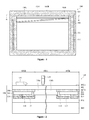
- the touch device 100 is, for example, a capacitive touch device, having a sensing area 100A and a peripheral area 100B surrounding the sensing area 100A.
- a plurality of sensing electrodes 106a and 106b are disposed at the sensing area 100A.
- the sensing electrodes 106a have a first strip-shaped pattern with a gradually decreased width from the left to the right of Fig. 1 .
- the sensing electrodes 106b have a second strip-shaped pattern with a gradually increased width from the left to the right of Fig. 1 .
- the sensing electrodes 106a and 106b are alternately arranged at the sensing area 100A.
- Signal conveying traces 112 are disposed at the wider sides of the sensing electrodes 106a and 106b.
- the signal conveying traces 112 are electrically connected with the sensing electrodes 106a and 106b.
- the electrical variations sensed by the sensing electrodes 106a and 106b are conveyed to a signal processor (not shown) of the touch device 100 through the signal conveying traces 112 for calculating the touch signals.
- the touch signals are conveyed to a display panel (not shown) of the touch device 100 and images are displayed on the display panel according to the touch signals.
- the combination of the sensing electrodes 106a and 106b and the signal conveying traces 112 is referred to as a touch-sensing layer.
- the signal conveying traces 112 are disposed at the peripheral area 100B of the touch device 100.
- a mask layer 104 for light shielding, an induced layer 108, and a conductive layer 114 are also disposed at the peripheral area 100B. From a top view, the mask layer 104, the induced layer 108, and the conductive layer 114 have a shape of a ring surrounding the sensing area 100A.
- the induced layer 108 can effectively shield the interference produced from the finger of a user to the signal conveying traces 112 at the peripheral area 100B.
- a capacitance is first produced between the finger of a user and the induced layer 108.
- the capacitance is conveyed to a ground terminal through the conductive layer 114 to achieve a shielding effect.
- conductive material used for the conductive layer 114 can reduce impedance of the induced layer 108, such that the conductive layer 114 can enhance the shielding effect of the induced layer 108.
- the combination of the induced layer 108 and the conductive layer 114 are referred to as a shielding layer.
- the shielding layer is disposed at the peripheral area 100B and separated from the above-mentioned touch-sensing layer.
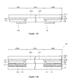
- the touch device 100 includes a touch panel 150 and a display panel 140.
- the display panel 140 is, for example, a liquid crystal display panel or other display elements.
- the display panel 140 may be attached under the touch panel 150 through an adhesive layer (not shown).
- the touch panel 150 includes a substrate 102, which can be used for a cover lens of the touch panel 150.
- the substrate 102 may be a transparent or an opaque substrate. When the substrate 102 is a transparent substrate, it can be applied to a touch panel with an image display effect.
- the material of the transparent substrate is such as a glass substrate. When the substrate 102 is an opaque substrate, it can be applied to a general touch pad.
- the substrate 102 has a first surface 102A and a second surface 102B which is opposite to the first surface 102A, wherein the first surface 102A is used as a touch side of the touch panel 150.
- the mask layer 104 is disposed at the peripheral area 100B on the second surface 102B of the substrate 102.
- the material of the mask layer 104 may be a colored photo-resist or a colored printing ink.
- the sensing electrodes 106a and 106b are disposed at the sensing area 100A on the second surface 102B of the substrate 102.
- the materials of the sensing electrodes 106a and 106b may be a transparent conductive material, such as indium tin oxide (ITO).
- ITO indium tin oxide
- the induced layer 108 is disposed at the peripheral area 100B, on the second surface 102B of the substrate 102.
- the materials of the induced layer 108 may be a transparent conductive material, such as indium tin oxide (ITO).
- ITO indium tin oxide
- the induced layer 108 is formed as a ring structure at the peripheral area 100B and separated from the sensing electrodes 106a and 106b.
- the signal conveying traces 112 is electrically connected with the sensing electrodes 106a and 106b and covered by the mask layer 104.
- An insulating layer 110 is disposed between the above-mentioned touch-sensing layer and the shielding layer.
- the insulating layer 110 electrically isolates the induced layer 108 from the signal conveying traces 112 and electrically isolates the induced layer 108 from the sensing electrodes 106a and 106b.
- the above-mentioned shielding layer is disposed between the mask layer 104 and the insulating layer 110.
- the conductive layer 114 is disposed on the induced layer 108 and electrically connected with the induced layer 108.
- the conductive layer 114 is also formed into a ring structure at the peripheral area 100B.
- the material of the conductive layer 114 may be a metal material. Since the transparent conductive material used for the induced layer 108 has high impedance, using the conductive layer 114 to electrically connect with the induced layer 108 can reduce the impedance of the induced layer 108 and enhance the shielding effect of the induced layer 108.
- a passivation layer 116 is blanketly formed on the second surface 102B of the substrate 102 to cover all components on the second surface 102B of the substrate 102, including the sensing electrodes 106a and 106b, the signal conveying traces 112, the induced layer 108, the conductive layer 114, and the mask layer 104.
- the material of the passivation layer 116 may be an organic or an inorganic material.
- the display panel 140 is provided under the touch panel 150 for bonding with the passivation layer 116 to form the touch device 100.
- the hand 132 of a user when one hand 132 of a user holds the touch device 100, the hand 132 of the user and the induced layer 108 produce capacitance. Then, the produced capacitance is conveyed to a ground terminal through the conductive layer 114. Therefore, the induced layer 108 effectively shields the interference produced from the hand 132 of the user to the signal conveying traces 112 at the peripheral area 100B.
- a substrate 102 is provided, having a first surface 102A and an opposite second surface 102B.
- the first surface 102A is used as a touch side of the touch panel 150.
- a mask layer 104 is formed at the peripheral area 100B on the second surface 102B of the substrate 102.
- the material of the mask layer 104 is, for example, a colored photo-resist or a colored printing ink, which can be patterned by a photolithography or a printing process to form the mask layer 104.
- a transparent conductive material layer is blanketly formed on the second surface 102B of the substrate 102. Then, the transparent conductive material layer is patterned by a photolithography and etching process or a printing process to form the sensing electrodes 106a and 106b at the sensing area 100A on the second surface 102B of the substrate 102 and form the induced layer 108 on the mask layer 104 at the peripheral area 100B.
- the sensing electrodes 106a and 106b are separated from the induced layer 108.
- the same process can form the sensing electrodes 106a and 106b and the induced layer 108 simultaneously.
- different processes can form the sensing electrodes 106a and 106b and the induced layer 108 separately.
- the insulating layer 110 is formed on the induced layer 108 and extends to a space between the sensing electrodes 106a and 106b and the induced layer 108.
- the material of the insulating layer 110 may be an organic or an inorganic insulating material, such as polyimide, which can be patterned by a photolithography or a printing process to form the insulating layer 110.
- the signal conveying traces 112 is formed on the insulating layer 110 and electrically connected to the sensing electrodes 106a and 106b.
- the conductive layer 114 is formed on the induced layer 108 and electrically connected with the induced layer 108.
- the materials of the signal conveying traces 112 and the conductive layer 114 may be a metal material, which can be patterned by a photolithography and etching process or a printing process to form the signal conveying traces 112 and the conductive layer 114.
- the signal conveying traces 112 and the conductive layer 114 can be formed simultaneously by the same process.
- the signal conveying traces 112 and the conductive layer 114 can be formed separately by different processes.
- the passivation layer 116 is blanketly formed over the second surface 102B of the substrate 102 to cover all components on the second surface 102B, including the sensing electrodes 106a and 106b, the signal conveying traces 112, the induced layer 108, the conductive layer 114, and the mask layer 104 to complete the fabrication of the touch panel 150.
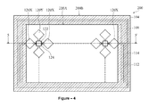
- the touch device 200 is, for example, a capacitive touch device, having a sensing area 200A and a peripheral area 200B surrounding the sensing area 200A.
- a plurality of first sensing electrodes 120Y arranged in columns and a plurality of second sensing electrodes 120X arranged in rows are disposed at the sensing area 200A.
- the first sensing electrodes 120Y arranged in a same column are connected with each other.
- the second sensing electrodes 120X arranged in a same row are separated from each other. Any two adjacent second sensing electrodes 120X arranged in a same row are connected together by a bridging line 124.
- an isolation portion 122 is disposed between the first sensing electrode 120Y and the bridging line 124 for electrically isolating the first sensing electrodes 120Y from the second sensing electrodes 120X.
- the electrical variations sensed by the second sensing electrodes 120X arranged in rows are conveyed to a signal processor (not shown) of the touch device 200 through the signal conveying traces 112 for calculating touch signals.
- the touch signals are conveyed to a display panel (not shown) of the touch device 200 through the signal conveying traces 112 for displaying images on the display panel according to the touch signals.
- first sensing electrodes 120Y arranged in columns
- electrical variations sensed by the first sensing electrodes 120Y arranged in columns can also be conveyed through other signal conveying traces (not shown).
- the combination of the first sensing electrodes 120Y, the second sensing electrodes 120X, the bridging line 124, and the signal conveying traces 112 is referred to as a touch-sensing layer.
- the signal conveying traces 112 are disposed at the peripheral area 200B of the touch device 200.
- a mask layer 104 for light shielding, an induced layer 108, and a conductive layer 114 are also disposed at the peripheral area 200B. From a top view, the mask layer 104, the induced layer 108, and the conductive layer 114 have the shape of a ring surrounding the sensing area 200A.
- the induced layer 108 can effectively shield the interference produced from the fingers of a user to the signal conveying traces 112 at the peripheral area 200B.
- a capacitance is first produced between the fingers of a user and the induced layer 108.
- the capacitance is conveyed to a ground terminal through the conductive layer 114 to achieve a shielding effect.
- the conductive material used for the conductive layer 114 can reduce impedance of the induced layer 108, such that the shielding effect of the induced layer 108 is enhanced.
- the combination of the induced layer 108 and the conductive layer 114 is referred to as a shielding layer.
- the shielding layer is disposed at the peripheral area 200B and separated from the above-mentioned touch-sensing layer.
- the touch device 200 includes a touch panel 250 and a display panel 140.
- the display panel 140 is, for example, a liquid crystal display panel or other display elements and attached under the touch panel 250.
- the touch panel 250 includes a substrate 102.
- the substrate 102 may be a transparent or an opaque substrate, which can be used for a cover lens of the touch panel 250.
- the substrate 102 is a transparent substrate, it can be applied to a touch panel having image display effect.
- the material of the transparent substrate is such as a glass plate.
- the substrate 102 is an opaque substrate, it can be applied to a general touch pad.
- the substrate 102 has a first surface 102A and an opposite second surface 102B, wherein the first surface 102A is used as a touch side of the touch panel 250.
- a mask layer 104 is disposed at the peripheral area 200B on the second surface 102B of the substrate 102.
- the material of the mask layer 104 may be a colored photo-resist or a colored printing ink.
- a plurality of first sensing electrodes 120Y and a plurality of second sensing electrodes 120X are disposed at the sensing area 200A on the second surface 102B of the substrate 102.
- the materials of the first sensing electrodes 120Y and the second sensing electrodes 120X may be a transparent conductive material, such as indium tin oxide (ITO).
- an insulating layer 110 is disposed between the above-mentioned touch-sensing layer and the shielding layer.
- the above-mentioned shielding layer is disposed between the mask layer 104 and the insulating layer 110.
- the induced layer 108 is disposed on the mask layer 104.
- the materials of the induced layer 108 may be a transparent conductive material, such as indium tin oxide (ITO).
- ITO indium tin oxide
- the induced layer 108 is formed as a ring structure at the peripheral area 200B and separated from the first sensing electrodes 120Y and the second sensing electrodes 120X.
- the insulating layer 110 is disposed on the induced layer 108 for electrically isolating the induced layer 108 from subsequently formed signal conveying traces 112.
- the insulating layer 110 further extends to a space between the induced layer 108 and the second sensing electrode 120X.
- an isolation portion 122 is disposed on the first sensing electrode 120Y for electrically isolating the first sensing electrode 120Y from a subsequently formed bridging line 124 which connects to the second sensing electrodes 120X.
- the signal conveying traces 112 is disposed on the insulating layer 110 and electrically connects to the second sensing electrode 120X.
- the bridging line 124 is disposed on the isolation portion 122 and electrically connects any two adjacent second sensing electrodes 120X together in the same row.
- the conductive layer 114 is disposed on the induced layer 108.
- the material of the conductive layer 114 may be a metal material. Because the transparent conductive material used for the induced layer 108 has high impedance, using the conductive layer 114 to electrically connect with the induced layer 108 can reduce the impedance of the induced layer 108 and enhance the shielding effect of the induced layer 108. As shown in Fig. 5 , when one hand 132 of a user holds the touch device 200, the hand 132 of the user and the induced layer 108 produces capacitance. Then, the produced capacitance is conveyed to a ground terminal through the conductive layer 114. Thus, the induced layer 108 effectively shields the interference produced from the hand 132 of a user to the signal conveying traces 112 at the peripheral area 200B.
- a passivation layer 116 is blanketly formed on the second surface 102B of the substrate 102 to cover all components on the second surface 102B, including the first sensing electrodes 120Y, the second sensing electrodes 120X, the signal conveying traces 112, the bridging line 124, the induced layer 108, the conductive layer 114, and the mask layer 104.
- the display panel 140 is provided under the touch panel 250 for bonding with the passivation layer 116, for example attached under the passivation layer 116 through an adhesive layer (not shown) to complete the touch device 200.
- a substrate 102 is provided.
- the substrate 102 has a first surface 102A and an opposite second surface 102B, wherein the first surface 102A is used as a touch side of the touch panel 250.
- a mask layer 104 is formed at the peripheral area 200B on the second surface 102B of the substrate 102.
- the material of the mask layer 104 is for example a colored photo-resist or a colored printing ink, which can be patterned by a photolithography or a printing process to form the mask layer 104.
- a transparent conductive material layer is blanketly formed on the second surface 102B of the substrate 102. Then, the transparent conductive material layer is patterned by a photolithography and etching process or a printing process to form the first sensing electrodes 120Y and the second sensing electrodes 120X at the sensing area 200A and form the induced layer 108 on the mask layer 104 at the peripheral area 200B.
- the first sensing electrodes 120Y and the second sensing electrodes 120X are separated from the induced layer 108.
- the same process can form the first sensing electrodes 120Y and the second sensing electrodes 120X and the induced layer 108 simultaneously.
- different processes can form the first sensing electrodes 120Y and the second sensing electrodes 120X and the induced layer 108 separately.
- the insulating layer 110 is formed on the induced layer 108 and extends to a space between the second sensing electrodes 120X and the induced layer 108.
- the isolation portion 122 is formed on the first sensing electrode 120Y and extends to a space between the first sensing electrode 120Y and the second sensing electrode 120X.
- the material of the insulating layer 110 and the isolation portion 122 may be an organic or an inorganic insulating material, such as polyimide, which can be patterned by a photolithography or a printing process to form the insulating layer 110 and the isolation portion 122. In an embodiment, the same process may form the insulating layer 110 and the isolation portion 122 simultaneously. In another embodiment, different processes may form the insulating layer 110 and the isolation portion 122 separately.
- the signal conveying traces 112 are formed on the insulating layer 110 and electrically connected to the second sensing electrode 120X.
- the bridging line 124 is formed on the isolation portion 122. Each bridging line 124 electrically connects any two adjacent second sensing electrodes 120X together in the same row.
- the conductive layer 114 is formed on the induced layer 108 and electrically connects with the induced layer 108.
- the materials of the signal conveying traces 112, the bridging line 124, and the conductive layer 114 may be a metal material, which can be patterned by a photolithography and etching process to form the signal conveying traces 112, the bridging line 124, and the conductive layer 114.
- the same process can form the signal conveying traces 112, the bridging line 124, and the conductive layer 114 simultaneously.
- different processes can form the signal conveying traces 112, the bridging line 124, and the conductive layer 114 separately.
- the passivation layer 116 is blanketly formed over the second surface 102B of the substrate 102 to cover all components on the second surface 102B, including the first sensing electrodes 120Y, the second sensing electrodes 120X, the signal conveying traces 112, the bridging line 124, the induced layer 108, the conductive layer 114, and the mask layer 104 to complete the fabrication of the touch panel 250.
- the induced layer 108 in the touch panels 150 and 250 can effectively shield the interference in the signal conveying traces 112 at the peripheral areas 100B and 200B, respectively.
- the conductive layer 114 electrically connecting to the induced layer 108 can reduce the impedance of the induced layer 108 to enhance the shielding effect of the induced layer 108. Accordingly, through the combination of the induced layer 108 and the conductive layer 114, the interference in the signal conveying traces 112 at the peripheral areas 100B and 200B can be shielded more effectively.
- the same process can form the induced layer 108 at the peripheral area 100B and the sensing electrodes 106a and 106b at the sensing area 100A simultaneously.
- the same process also can form the conductive layer 114 and the signal conveying traces 112 simultaneously. Therefore, compared with the processes for fabricating the conventional touch panels, the touch panel 150 of the embodiment of the invention only requires one added process step of forming the insulating layer 110 to complete the fabrication of the touch panel 150 and achieve an excellent shielding effect at the same time.
- the induced layer 108 at the peripheral area 200B and the first sensing electrodes 120Y and the second sensing electrodes 120X at the sensing area 200A can be formed simultaneously by the same process.
- the same process also can form the conductive layer 114, the signal conveying traces 112, and the bridging line 124 simultaneously.
- the same process also can form the insulating layer 110 and the isolation portion 122 at the sensing area 200A simultaneously. Therefore, compared with the processes for fabricating the conventional touch panels, the touch panel 250 of the embodiment of the invention does not require any extra process step to complete the fabrication of the touch panel 250 and achieve excellent shielding effect at the same time.
Landscapes
- Engineering & Computer Science (AREA)
- General Engineering & Computer Science (AREA)
- Theoretical Computer Science (AREA)
- Human Computer Interaction (AREA)
- Physics & Mathematics (AREA)
- General Physics & Mathematics (AREA)
- Position Input By Displaying (AREA)
- Solid State Image Pick-Up Elements (AREA)
Applications Claiming Priority (1)
| Application Number | Priority Date | Filing Date | Title |
|---|---|---|---|
| CN201110077947.9A CN102681712B (zh) | 2011-03-18 | 2011-03-18 | 触控装置及其制造方法 |
Publications (2)
| Publication Number | Publication Date |
|---|---|
| EP2500803A2 true EP2500803A2 (fr) | 2012-09-19 |
| EP2500803A3 EP2500803A3 (fr) | 2014-02-26 |
Family
ID=44789311
Family Applications (1)
| Application Number | Title | Priority Date | Filing Date |
|---|---|---|---|
| EP11178253.8A Ceased EP2500803A3 (fr) | 2011-03-18 | 2011-08-22 | Dispositif tactile et son procédé de fabrication |
Country Status (6)
| Country | Link |
|---|---|
| US (1) | US8952903B2 (fr) |
| EP (1) | EP2500803A3 (fr) |
| JP (1) | JP5502919B2 (fr) |
| KR (1) | KR101365180B1 (fr) |
| CN (1) | CN102681712B (fr) |
| TW (2) | TWM414620U (fr) |
Cited By (4)
| Publication number | Priority date | Publication date | Assignee | Title |
|---|---|---|---|---|
| CN103455204A (zh) * | 2013-08-30 | 2013-12-18 | 京东方科技集团股份有限公司 | 触摸屏、其制作方法及显示装置 |
| US9433102B2 (en) | 2013-08-30 | 2016-08-30 | Boe Technology Group Co., Ltd. | Touch screen panel and method for manufacturing the same, and display device |
| US9430109B2 (en) | 2013-08-30 | 2016-08-30 | Boe Technology Group Co., Ltd. | Touch screen panel and method for manufacturing the same, and display device |
| EP2713249B1 (fr) * | 2012-09-28 | 2017-08-09 | HTC Corporation | Module d'affichage tactile et appareil électronique portatif |
Families Citing this family (35)
| Publication number | Priority date | Publication date | Assignee | Title |
|---|---|---|---|---|
| CN102681709B (zh) * | 2011-03-17 | 2016-01-27 | 宸鸿光电科技股份有限公司 | 触控显示设备及其制造方法 |
| CN103049121B (zh) * | 2011-10-13 | 2016-04-06 | 宸鸿科技(厦门)有限公司 | 触控装置及其制造方法 |
| TWM425340U (en) * | 2011-10-21 | 2012-03-21 | Henghao Technology Co Ltd | Capacitive touch panel and touch display panel using the same |
| JP5189197B1 (ja) * | 2011-10-27 | 2013-04-24 | シャープ株式会社 | 携帯情報端末 |
| US9429608B2 (en) * | 2011-11-11 | 2016-08-30 | Plantronics, Inc. | Separation of capacitive touch areas |
| CN103164069B (zh) * | 2011-12-19 | 2016-02-24 | 瀚宇彩晶股份有限公司 | 触控装置及其制造方法 |
| JP6014055B2 (ja) * | 2012-01-18 | 2016-10-25 | 京セラ株式会社 | 入力装置、表示装置、および電子機器 |
| JP2013152562A (ja) * | 2012-01-24 | 2013-08-08 | Japan Display West Co Ltd | タッチパネルおよびその製造方法、表示装置、ならびに電子機器 |
| GB2499987B (en) * | 2012-03-02 | 2017-01-11 | Novalia Ltd | Touch-sensitive input device |
| CN103425301B (zh) * | 2012-05-16 | 2016-10-05 | 宸鸿科技(厦门)有限公司 | 触控面板及其制作方法 |
| JP2015180979A (ja) * | 2012-07-31 | 2015-10-15 | シャープ株式会社 | タッチパネルおよびタッチパネルの製造方法 |
| CN104781764B (zh) * | 2012-10-29 | 2017-07-18 | 夏普株式会社 | 触摸面板 |
| CN103092411A (zh) * | 2013-01-10 | 2013-05-08 | 北京京东方光电科技有限公司 | 一种触摸屏及其制作方法、显示装置 |
| JP5588525B2 (ja) * | 2013-01-22 | 2014-09-10 | 志忠 林 | タッチパネルの製造方法 |
| TWI498780B (zh) * | 2013-01-22 | 2015-09-01 | Henghao Technology Co Ltd | 觸控面板 |
| TWI488084B (zh) * | 2013-02-08 | 2015-06-11 | Acer Inc | 觸控面板 |
| JP2014154088A (ja) * | 2013-02-13 | 2014-08-25 | Geomatec Co Ltd | 保護パネル一体型タッチパネルセンサ,その製造方法及び携帯用電子機器 |
| CN104007864B (zh) * | 2013-02-27 | 2017-09-12 | 宸鸿科技(厦门)有限公司 | 触控面板及其制作方法 |
| CN103176660B (zh) * | 2013-03-28 | 2015-09-30 | 南昌欧菲光科技有限公司 | 位置传感器 |
| US9606679B2 (en) | 2013-04-23 | 2017-03-28 | Industrial Technology Research Institute | Touch panel and manufacturing method thereof and touch display panel |
| JP6108098B2 (ja) * | 2013-05-17 | 2017-04-05 | 大日本印刷株式会社 | 配線付き表示装置用前面保護板とその製造方法、及び表示装置 |
| TWI486841B (zh) | 2013-06-26 | 2015-06-01 | Young Lighting Technology Inc | 觸控模組 |
| FR3008809B1 (fr) | 2013-07-18 | 2017-07-07 | Fogale Nanotech | Dispositif accessoire garde pour un appareil electronique et/ou informatique, et appareil equipe d'un tel dispositif accessoire |
| CN103500036B (zh) | 2013-08-30 | 2015-04-29 | 京东方科技集团股份有限公司 | 触摸屏的制作方法 |
| CN103455203A (zh) * | 2013-08-30 | 2013-12-18 | 京东方科技集团股份有限公司 | 触摸屏、其制作方法及显示装置 |
| KR102119818B1 (ko) * | 2013-09-24 | 2020-06-05 | 엘지이노텍 주식회사 | 터치 패널 |
| US9292141B2 (en) * | 2013-10-30 | 2016-03-22 | Apple Inc. | Double sided touch sensor on transparent substrate |
| FR3013472B1 (fr) | 2013-11-19 | 2016-07-08 | Fogale Nanotech | Dispositif accessoire couvrant pour un appareil portable electronique et/ou informatique, et appareil equipe d'un tel dispositif accessoire |
| TW201545030A (zh) * | 2014-05-30 | 2015-12-01 | Henghao Technology Co Ltd | 觸控面板及其形成方法 |
| CN105528122A (zh) * | 2014-09-29 | 2016-04-27 | 宸鸿科技(厦门)有限公司 | 触控面板及其制造方法 |
| CN105786230B (zh) * | 2014-12-23 | 2019-08-13 | 宸鸿科技(厦门)有限公司 | 触控面板及其制造方法 |
| CN105653107B (zh) * | 2015-12-28 | 2020-09-01 | 昆山龙腾光电股份有限公司 | 触控装置、电子装置以及手机 |
| KR102512040B1 (ko) * | 2016-05-04 | 2023-03-20 | 엘지디스플레이 주식회사 | 플렉서블 디스플레이 패널 및 그 제조 방법 |
| CN106843616B (zh) * | 2017-01-03 | 2020-05-19 | 京东方科技集团股份有限公司 | 一种触控基板及其制作方法、触控显示装置 |
| CN110389686B (zh) * | 2019-07-25 | 2023-09-08 | 京东方科技集团股份有限公司 | 一种触控器件、显示装置以及触控器件的制备方法 |
Citations (1)
| Publication number | Priority date | Publication date | Assignee | Title |
|---|---|---|---|---|
| US20100220071A1 (en) * | 2009-02-20 | 2010-09-02 | Kiyoshi Nishihara | Touch panel and display device including the same |
Family Cites Families (20)
| Publication number | Priority date | Publication date | Assignee | Title |
|---|---|---|---|---|
| US5548306A (en) * | 1994-04-28 | 1996-08-20 | At&T Global Information Solutions Company | Visible and touchable touch screen shield |
| US5579036A (en) * | 1994-04-28 | 1996-11-26 | At&T Global Information Solutions Company | Touch screen device and shielding bracket therefor |
| KR100659048B1 (ko) * | 2000-09-06 | 2006-12-18 | 삼성에스디아이 주식회사 | 외부 노이즈를 차단할 수 있는 더미전극을 구비한 터치패널 |
| CN101449461B (zh) * | 2006-03-13 | 2013-06-12 | 艾登特技术股份公司 | 电容传感器设备 |
| TW200805128A (en) * | 2006-05-05 | 2008-01-16 | Harald Philipp | Touch screen element |
| US20080001926A1 (en) * | 2006-06-29 | 2008-01-03 | Xiaoping Jiang | Bidirectional slider |
| US8610690B2 (en) * | 2007-07-27 | 2013-12-17 | Tpk Touch Solutions Inc. | Capacitive sensor and method for manufacturing same |
| KR100921813B1 (ko) * | 2007-11-07 | 2009-10-16 | 주식회사 애트랩 | 터치 패널 장치 및 이의 접촉위치 검출방법 |
| JP2009169720A (ja) * | 2008-01-17 | 2009-07-30 | Smk Corp | タッチセンサ |
| TWM348999U (en) | 2008-02-18 | 2009-01-11 | Tpk Touch Solutions Inc | Capacitive touch panel |
| CN201174007Y (zh) | 2008-03-18 | 2008-12-31 | 宸鸿光电科技股份有限公司 | 电容式触控面板 |
| US8629842B2 (en) * | 2008-07-11 | 2014-01-14 | Samsung Display Co., Ltd. | Organic light emitting display device |
| KR20100065486A (ko) * | 2008-12-08 | 2010-06-17 | 주식회사 엔에이치케이플러스 | 정전용량 방식의 터치 패널 구조 |
| TWI373665B (en) * | 2008-12-25 | 2012-10-01 | Au Optronics Corp | Touch panel structure |
| TWM361675U (en) | 2009-02-24 | 2009-07-21 | Sentelic Corp | Thin film touch panel |
| CN201387599Y (zh) | 2009-03-05 | 2010-01-20 | 升达科技股份有限公司 | 薄膜触控板 |
| CN201465086U (zh) | 2009-07-03 | 2010-05-12 | 深圳市汇顶科技有限公司 | 一种抗干扰的电容式触摸屏及电子设备 |
| JP5300640B2 (ja) * | 2009-07-27 | 2013-09-25 | 株式会社ジャパンディスプレイウェスト | 静電容量型入力装置および入力装置付き電気光学装置 |
| JP4926218B2 (ja) * | 2009-08-28 | 2012-05-09 | 京セラ株式会社 | 入力装置およびこれを備える表示装置 |
| CN202041932U (zh) * | 2011-03-18 | 2011-11-16 | 宸鸿科技(厦门)有限公司 | 触控装置 |
-
2011
- 2011-03-18 CN CN201110077947.9A patent/CN102681712B/zh not_active Expired - Fee Related
- 2011-05-31 TW TW100209811U patent/TWM414620U/zh not_active IP Right Cessation
- 2011-05-31 TW TW100118980A patent/TWI459254B/zh not_active IP Right Cessation
- 2011-08-09 US US13/205,630 patent/US8952903B2/en active Active
- 2011-08-22 EP EP11178253.8A patent/EP2500803A3/fr not_active Ceased
- 2011-08-31 KR KR1020110088016A patent/KR101365180B1/ko not_active Expired - Fee Related
-
2012
- 2012-03-08 JP JP2012051643A patent/JP5502919B2/ja not_active Expired - Fee Related
Patent Citations (1)
| Publication number | Priority date | Publication date | Assignee | Title |
|---|---|---|---|---|
| US20100220071A1 (en) * | 2009-02-20 | 2010-09-02 | Kiyoshi Nishihara | Touch panel and display device including the same |
Cited By (5)
| Publication number | Priority date | Publication date | Assignee | Title |
|---|---|---|---|---|
| EP2713249B1 (fr) * | 2012-09-28 | 2017-08-09 | HTC Corporation | Module d'affichage tactile et appareil électronique portatif |
| CN103455204A (zh) * | 2013-08-30 | 2013-12-18 | 京东方科技集团股份有限公司 | 触摸屏、其制作方法及显示装置 |
| CN103455204B (zh) * | 2013-08-30 | 2016-08-17 | 京东方科技集团股份有限公司 | 触摸屏、其制作方法及显示装置 |
| US9433102B2 (en) | 2013-08-30 | 2016-08-30 | Boe Technology Group Co., Ltd. | Touch screen panel and method for manufacturing the same, and display device |
| US9430109B2 (en) | 2013-08-30 | 2016-08-30 | Boe Technology Group Co., Ltd. | Touch screen panel and method for manufacturing the same, and display device |
Also Published As
| Publication number | Publication date |
|---|---|
| CN102681712B (zh) | 2016-08-24 |
| US20120235927A1 (en) | 2012-09-20 |
| TW201239700A (en) | 2012-10-01 |
| TWI459254B (zh) | 2014-11-01 |
| KR101365180B1 (ko) | 2014-02-21 |
| JP5502919B2 (ja) | 2014-05-28 |
| EP2500803A3 (fr) | 2014-02-26 |
| JP2012198885A (ja) | 2012-10-18 |
| CN102681712A (zh) | 2012-09-19 |
| TWM414620U (en) | 2011-10-21 |
| KR20120106526A (ko) | 2012-09-26 |
| US8952903B2 (en) | 2015-02-10 |
Similar Documents
| Publication | Publication Date | Title |
|---|---|---|
| US8952903B2 (en) | Touch device and fabrication method thereof | |
| US8269743B2 (en) | Touch sensing display panel and touch sensing substrate | |
| US8289296B2 (en) | Touch screen panel | |
| US9454267B2 (en) | Touch sensing circuit and method for making the same | |
| TWI559192B (zh) | 觸控顯示裝置及其驅動方法 | |
| KR101542043B1 (ko) | 터치 스크린 패널 | |
| US20140347319A1 (en) | Touch panel | |
| US20140368755A1 (en) | Touch panel | |
| US20100283762A1 (en) | Display device, electronic equipment provided with the display device, and touch panel | |
| US20100283757A1 (en) | Capacitive touch panel structure with high optical uniformity | |
| JP2011186717A (ja) | 静電容量型タッチパネルとその製造方法 | |
| JP6539190B2 (ja) | タッチ検出装置及びタッチ検出機能付き表示装置 | |
| CN205880425U (zh) | 显示面板及显示装置 | |
| CN106371653A (zh) | 显示装置、输入装置及显示装置的制造方法 | |
| US20160034076A1 (en) | Touch display device | |
| TWM454579U (zh) | 觸控面板 | |
| CN109814758B (zh) | 触控基板、触控驱动方法和电子装置 | |
| KR101703503B1 (ko) | 회로기판을 이용하여 터치센서 칩에 감지 신호를 전달하는 접촉 감지 패널 및 접촉 감지 장치 | |
| EP2713249B1 (fr) | Module d'affichage tactile et appareil électronique portatif | |
| CN202041932U (zh) | 触控装置 | |
| JP2014170334A (ja) | 静電容量式タッチパネルおよびそれを用いた手持ち式電子機器 | |
| US9389741B2 (en) | Touch panel and a method of forming the same | |
| KR102281616B1 (ko) | 터치 스크린 패널 및 터치 스크린 패널 제조 방법 | |
| KR102050448B1 (ko) | 터치감지장치 및 그의 제조방법 | |
| US20160103509A1 (en) | Touch display device |
Legal Events
| Date | Code | Title | Description |
|---|---|---|---|
| PUAI | Public reference made under article 153(3) epc to a published international application that has entered the european phase |
Free format text: ORIGINAL CODE: 0009012 |
|
| AK | Designated contracting states |
Kind code of ref document: A2 Designated state(s): AL AT BE BG CH CY CZ DE DK EE ES FI FR GB GR HR HU IE IS IT LI LT LU LV MC MK MT NL NO PL PT RO RS SE SI SK SM TR |
|
| AX | Request for extension of the european patent |
Extension state: BA ME |
|
| PUAL | Search report despatched |
Free format text: ORIGINAL CODE: 0009013 |
|
| AK | Designated contracting states |
Kind code of ref document: A3 Designated state(s): AL AT BE BG CH CY CZ DE DK EE ES FI FR GB GR HR HU IE IS IT LI LT LU LV MC MK MT NL NO PL PT RO RS SE SI SK SM TR |
|
| AX | Request for extension of the european patent |
Extension state: BA ME |
|
| RIC1 | Information provided on ipc code assigned before grant |
Ipc: G06F 3/044 20060101AFI20140121BHEP |
|
| 17P | Request for examination filed |
Effective date: 20140825 |
|
| 17Q | First examination report despatched |
Effective date: 20150402 |
|
| STAA | Information on the status of an ep patent application or granted ep patent |
Free format text: STATUS: EXAMINATION IS IN PROGRESS |
|
| STAA | Information on the status of an ep patent application or granted ep patent |
Free format text: STATUS: THE APPLICATION HAS BEEN REFUSED |
|
| 18R | Application refused |
Effective date: 20190619 |