EP2501842B1 - Verfahren zur räumlich aufgelösten vergrösserung von nanopartikeln auf einer substratoberfläche - Google Patents
Verfahren zur räumlich aufgelösten vergrösserung von nanopartikeln auf einer substratoberfläche Download PDFInfo
- Publication number
- EP2501842B1 EP2501842B1 EP10778575.0A EP10778575A EP2501842B1 EP 2501842 B1 EP2501842 B1 EP 2501842B1 EP 10778575 A EP10778575 A EP 10778575A EP 2501842 B1 EP2501842 B1 EP 2501842B1
- Authority
- EP
- European Patent Office
- Prior art keywords
- precious metal
- substrate
- metal nanoparticles
- substrate surface
- nanoparticles
- Prior art date
- Legal status (The legal status is an assumption and is not a legal conclusion. Google has not performed a legal analysis and makes no representation as to the accuracy of the status listed.)
- Active
Links
Images


Classifications
-
- C—CHEMISTRY; METALLURGY
- C23—COATING METALLIC MATERIAL; COATING MATERIAL WITH METALLIC MATERIAL; CHEMICAL SURFACE TREATMENT; DIFFUSION TREATMENT OF METALLIC MATERIAL; COATING BY VACUUM EVAPORATION, BY SPUTTERING, BY ION IMPLANTATION OR BY CHEMICAL VAPOUR DEPOSITION, IN GENERAL; INHIBITING CORROSION OF METALLIC MATERIAL OR INCRUSTATION IN GENERAL
- C23C—COATING METALLIC MATERIAL; COATING MATERIAL WITH METALLIC MATERIAL; SURFACE TREATMENT OF METALLIC MATERIAL BY DIFFUSION INTO THE SURFACE, BY CHEMICAL CONVERSION OR SUBSTITUTION; COATING BY VACUUM EVAPORATION, BY SPUTTERING, BY ION IMPLANTATION OR BY CHEMICAL VAPOUR DEPOSITION, IN GENERAL
- C23C18/00—Chemical coating by decomposition of either liquid compounds or solutions of the coating forming compounds, without leaving reaction products of surface material in the coating; Contact plating
- C23C18/16—Chemical coating by decomposition of either liquid compounds or solutions of the coating forming compounds, without leaving reaction products of surface material in the coating; Contact plating by reduction or substitution, e.g. electroless plating
- C23C18/1601—Process or apparatus
- C23C18/1603—Process or apparatus coating on selected surface areas
- C23C18/1605—Process or apparatus coating on selected surface areas by masking
-
- C—CHEMISTRY; METALLURGY
- C23—COATING METALLIC MATERIAL; COATING MATERIAL WITH METALLIC MATERIAL; CHEMICAL SURFACE TREATMENT; DIFFUSION TREATMENT OF METALLIC MATERIAL; COATING BY VACUUM EVAPORATION, BY SPUTTERING, BY ION IMPLANTATION OR BY CHEMICAL VAPOUR DEPOSITION, IN GENERAL; INHIBITING CORROSION OF METALLIC MATERIAL OR INCRUSTATION IN GENERAL
- C23C—COATING METALLIC MATERIAL; COATING MATERIAL WITH METALLIC MATERIAL; SURFACE TREATMENT OF METALLIC MATERIAL BY DIFFUSION INTO THE SURFACE, BY CHEMICAL CONVERSION OR SUBSTITUTION; COATING BY VACUUM EVAPORATION, BY SPUTTERING, BY ION IMPLANTATION OR BY CHEMICAL VAPOUR DEPOSITION, IN GENERAL
- C23C18/00—Chemical coating by decomposition of either liquid compounds or solutions of the coating forming compounds, without leaving reaction products of surface material in the coating; Contact plating
- C23C18/16—Chemical coating by decomposition of either liquid compounds or solutions of the coating forming compounds, without leaving reaction products of surface material in the coating; Contact plating by reduction or substitution, e.g. electroless plating
- C23C18/1601—Process or apparatus
- C23C18/1603—Process or apparatus coating on selected surface areas
- C23C18/1607—Process or apparatus coating on selected surface areas by direct patterning
- C23C18/1612—Process or apparatus coating on selected surface areas by direct patterning through irradiation means
-
- C—CHEMISTRY; METALLURGY
- C23—COATING METALLIC MATERIAL; COATING MATERIAL WITH METALLIC MATERIAL; CHEMICAL SURFACE TREATMENT; DIFFUSION TREATMENT OF METALLIC MATERIAL; COATING BY VACUUM EVAPORATION, BY SPUTTERING, BY ION IMPLANTATION OR BY CHEMICAL VAPOUR DEPOSITION, IN GENERAL; INHIBITING CORROSION OF METALLIC MATERIAL OR INCRUSTATION IN GENERAL
- C23C—COATING METALLIC MATERIAL; COATING MATERIAL WITH METALLIC MATERIAL; SURFACE TREATMENT OF METALLIC MATERIAL BY DIFFUSION INTO THE SURFACE, BY CHEMICAL CONVERSION OR SUBSTITUTION; COATING BY VACUUM EVAPORATION, BY SPUTTERING, BY ION IMPLANTATION OR BY CHEMICAL VAPOUR DEPOSITION, IN GENERAL
- C23C18/00—Chemical coating by decomposition of either liquid compounds or solutions of the coating forming compounds, without leaving reaction products of surface material in the coating; Contact plating
- C23C18/16—Chemical coating by decomposition of either liquid compounds or solutions of the coating forming compounds, without leaving reaction products of surface material in the coating; Contact plating by reduction or substitution, e.g. electroless plating
- C23C18/1601—Process or apparatus
- C23C18/1633—Process of electroless plating
- C23C18/1655—Process features
- C23C18/1664—Process features with additional means during the plating process
- C23C18/1667—Radiant energy, e.g. laser
-
- C—CHEMISTRY; METALLURGY
- C23—COATING METALLIC MATERIAL; COATING MATERIAL WITH METALLIC MATERIAL; CHEMICAL SURFACE TREATMENT; DIFFUSION TREATMENT OF METALLIC MATERIAL; COATING BY VACUUM EVAPORATION, BY SPUTTERING, BY ION IMPLANTATION OR BY CHEMICAL VAPOUR DEPOSITION, IN GENERAL; INHIBITING CORROSION OF METALLIC MATERIAL OR INCRUSTATION IN GENERAL
- C23C—COATING METALLIC MATERIAL; COATING MATERIAL WITH METALLIC MATERIAL; SURFACE TREATMENT OF METALLIC MATERIAL BY DIFFUSION INTO THE SURFACE, BY CHEMICAL CONVERSION OR SUBSTITUTION; COATING BY VACUUM EVAPORATION, BY SPUTTERING, BY ION IMPLANTATION OR BY CHEMICAL VAPOUR DEPOSITION, IN GENERAL
- C23C18/00—Chemical coating by decomposition of either liquid compounds or solutions of the coating forming compounds, without leaving reaction products of surface material in the coating; Contact plating
- C23C18/16—Chemical coating by decomposition of either liquid compounds or solutions of the coating forming compounds, without leaving reaction products of surface material in the coating; Contact plating by reduction or substitution, e.g. electroless plating
- C23C18/18—Pretreatment of the material to be coated
- C23C18/1803—Pretreatment of the material to be coated of metallic material surfaces or of a non-specific material surfaces
- C23C18/1824—Pretreatment of the material to be coated of metallic material surfaces or of a non-specific material surfaces by chemical pretreatment
- C23C18/1837—Multistep pretreatment
- C23C18/1841—Multistep pretreatment with use of metal first
-
- C—CHEMISTRY; METALLURGY
- C23—COATING METALLIC MATERIAL; COATING MATERIAL WITH METALLIC MATERIAL; CHEMICAL SURFACE TREATMENT; DIFFUSION TREATMENT OF METALLIC MATERIAL; COATING BY VACUUM EVAPORATION, BY SPUTTERING, BY ION IMPLANTATION OR BY CHEMICAL VAPOUR DEPOSITION, IN GENERAL; INHIBITING CORROSION OF METALLIC MATERIAL OR INCRUSTATION IN GENERAL
- C23C—COATING METALLIC MATERIAL; COATING MATERIAL WITH METALLIC MATERIAL; SURFACE TREATMENT OF METALLIC MATERIAL BY DIFFUSION INTO THE SURFACE, BY CHEMICAL CONVERSION OR SUBSTITUTION; COATING BY VACUUM EVAPORATION, BY SPUTTERING, BY ION IMPLANTATION OR BY CHEMICAL VAPOUR DEPOSITION, IN GENERAL
- C23C18/00—Chemical coating by decomposition of either liquid compounds or solutions of the coating forming compounds, without leaving reaction products of surface material in the coating; Contact plating
- C23C18/16—Chemical coating by decomposition of either liquid compounds or solutions of the coating forming compounds, without leaving reaction products of surface material in the coating; Contact plating by reduction or substitution, e.g. electroless plating
- C23C18/18—Pretreatment of the material to be coated
- C23C18/1851—Pretreatment of the material to be coated of surfaces of non-metallic or semiconducting in organic material
- C23C18/1872—Pretreatment of the material to be coated of surfaces of non-metallic or semiconducting in organic material by chemical pretreatment
- C23C18/1886—Multistep pretreatment
- C23C18/1889—Multistep pretreatment with use of metal first
-
- C—CHEMISTRY; METALLURGY
- C23—COATING METALLIC MATERIAL; COATING MATERIAL WITH METALLIC MATERIAL; CHEMICAL SURFACE TREATMENT; DIFFUSION TREATMENT OF METALLIC MATERIAL; COATING BY VACUUM EVAPORATION, BY SPUTTERING, BY ION IMPLANTATION OR BY CHEMICAL VAPOUR DEPOSITION, IN GENERAL; INHIBITING CORROSION OF METALLIC MATERIAL OR INCRUSTATION IN GENERAL
- C23C—COATING METALLIC MATERIAL; COATING MATERIAL WITH METALLIC MATERIAL; SURFACE TREATMENT OF METALLIC MATERIAL BY DIFFUSION INTO THE SURFACE, BY CHEMICAL CONVERSION OR SUBSTITUTION; COATING BY VACUUM EVAPORATION, BY SPUTTERING, BY ION IMPLANTATION OR BY CHEMICAL VAPOUR DEPOSITION, IN GENERAL
- C23C18/00—Chemical coating by decomposition of either liquid compounds or solutions of the coating forming compounds, without leaving reaction products of surface material in the coating; Contact plating
- C23C18/16—Chemical coating by decomposition of either liquid compounds or solutions of the coating forming compounds, without leaving reaction products of surface material in the coating; Contact plating by reduction or substitution, e.g. electroless plating
- C23C18/31—Coating with metals
- C23C18/42—Coating with noble metals
- C23C18/44—Coating with noble metals using reducing agents
-
- Y—GENERAL TAGGING OF NEW TECHNOLOGICAL DEVELOPMENTS; GENERAL TAGGING OF CROSS-SECTIONAL TECHNOLOGIES SPANNING OVER SEVERAL SECTIONS OF THE IPC; TECHNICAL SUBJECTS COVERED BY FORMER USPC CROSS-REFERENCE ART COLLECTIONS [XRACs] AND DIGESTS
- Y10—TECHNICAL SUBJECTS COVERED BY FORMER USPC
- Y10T—TECHNICAL SUBJECTS COVERED BY FORMER US CLASSIFICATION
- Y10T428/00—Stock material or miscellaneous articles
- Y10T428/24—Structurally defined web or sheet [e.g., overall dimension, etc.]
- Y10T428/24479—Structurally defined web or sheet [e.g., overall dimension, etc.] including variation in thickness
- Y10T428/24612—Composite web or sheet
-
- Y—GENERAL TAGGING OF NEW TECHNOLOGICAL DEVELOPMENTS; GENERAL TAGGING OF CROSS-SECTIONAL TECHNOLOGIES SPANNING OVER SEVERAL SECTIONS OF THE IPC; TECHNICAL SUBJECTS COVERED BY FORMER USPC CROSS-REFERENCE ART COLLECTIONS [XRACs] AND DIGESTS
- Y10—TECHNICAL SUBJECTS COVERED BY FORMER USPC
- Y10T—TECHNICAL SUBJECTS COVERED BY FORMER US CLASSIFICATION
- Y10T428/00—Stock material or miscellaneous articles
- Y10T428/24—Structurally defined web or sheet [e.g., overall dimension, etc.]
- Y10T428/24802—Discontinuous or differential coating, impregnation or bond [e.g., artwork, printing, retouched photograph, etc.]
- Y10T428/24893—Discontinuous or differential coating, impregnation or bond [e.g., artwork, printing, retouched photograph, etc.] including particulate material
- Y10T428/24909—Free metal or mineral containing
Definitions
- the present invention relates to methods for spatially resolved magnification and size fine tuning of noble metal nanoparticles on a substrate surface, and to the nanoparticle assemblies and nanostructured substrate surfaces so prepared and their use.
- nanostructures especially ordered structures of noble metal nanoparticles on substrate surfaces, have found great interest in a variety of applications in various fields.
- gold nanoparticles can be used in biochemical sensors ( Dyckman and Bogatyrev (2007), Russian Chemical Reviews 76 (2), 181-194 ) and as etching masks for the production of biomimetic interfaces and interfaces ( Lohmüller et al. (2008), NANO LETTERS 8 (5): 1429-1433 ).
- noble metal nanoparticles of given diameters could also be advantageously used in new transistors (Sato et al. (1997), American Institute of Physics 82 (2), 696-702) or for fluorescence quenching (US Pat. Fan et al. (2003), PNAS, 100 (1), 6297-6301 ) be used.
- the size of noble metal nanoparticles, in particular gold nanoparticles can in principle be applied before application to the substrate surface, eg when using metal colloids (US Pat. Kimling et al. (2006) J. Phys. Chem. B., 110, 15700-15707 ), or after application, eg by electroless deposition using a reducing agent ( Hrapovic et al.
- particle size gradients are generated either by electroless deposition from a solution containing elemental gold as above, but varying the rate at which a nanoparticle-coated substrate surface is withdrawn from this solution or by irradiation with a laterally intensity-modulated light field.
- a related task was to provide the appropriate nanoparticle assemblies and nanostructured substrate surfaces.
- a further object was the provision of the nanoparticle arrangements and nanostructured substrate surfaces prepared according to the invention for various uses which hitherto were not suitable for such noble metal nanoparticle arrangements owing to the inadequate or inadequate size possible fine adjustment of noble metal nanoparticles on a substrate surface.
- the above-mentioned main object can be achieved by providing the method according to claim 1, in which a substrate coated with (preferably fixed) noble metal nanoparticles is contacted with a noble metal salt solution and localized by UV irradiation of certain predetermined areas and controlled enlargement of the nanoparticles in these areas is initiated.
- a substrate coated with (preferably fixed) noble metal nanoparticles is contacted with a noble metal salt solution and localized by UV irradiation of certain predetermined areas and controlled enlargement of the nanoparticles in these areas is initiated.
- EP 1 626 106 A2 For example, a dried metal colloid film is subjected to laser irradiation.
- the laser irradiation is not used for reduction, but for removal of molecules of the dispersion medium, which initially keep the fine metal particles separated. After removal, aggregation and formation of larger metal particles occurs.
- EP 1760 527 A1 discloses the irradiation of a polymer film on a substrate to fix or chemically modify the polymer components of that film.
- a substrate coated with noble metal nanoparticles in the above step a) can in principle be carried out by all methods known in the prior art.
- a noble metal colloid layer can be applied to the substrate surface (see Hrapovic et al., Supra).
- Another preferred method according to the invention is the production of a noble metal nanoparticle arrangement on a substrate by micellar nanolithography, more particularly micellar block copolymer nanolithography (BCML) (see, for example, US Pat EP 1 027 157 ).
- micellar block copolymer nanolithography a micellar solution of a block copolymer is deposited on a substrate, for example by dip coating, and forms, under suitable conditions on the surface, an ordered film structure of chemically distinct polymer domains including, but not limited to, type, molecular weight, and concentration Block copolymer depends.
- the micelles in the solution can be loaded with inorganic salts, which can be reduced to inorganic nanoparticles after deposition with the polymer film.
- a plasma treatment for example with hydrogen plasma, is generally carried out.
- the substrate material used in the invention is basically not particularly limited and may include any material as long as it is stable under the conditions of the process of the present invention and does not interfere with or interfere with the reactions taking place.
- the substrate can be made, for example, of glass, SiO 2 , silicon, metals (with or without passivated surfaces), semiconductor materials, eg GaAs, GaP, GaInP, AlGaAs, (optionally doped) metal oxides, eg ZnO, TiO 2 , carbon (graphite , Diamond), polymers, etc., and composite materials thereof.
- transparent substrates such as glass or ITO on glass are preferred.
- the noble metal of the nanoparticles is not particularly limited and may include any noble metal known in the art for such nanoparticles, or composites of plural noble metals (hybrid particles) or mixtures of a noble metal with another metal.
- the noble metal is selected from the group consisting of Au, Pt, Pd, Ag or mixtures / composites of these metals and most preferably is gold.
- the original nanoparticles typically have diameters in the range of 1 nm to 100 nm, preferably 4 nm to 30 nm.
- the interparticle distances can be varied over a wide range as desired, for example in one Range of 20 to 1000 nm, typically in the range of 30 to 250 nm.
- the substrate may, if necessary, after the application of the nanoparticles, but before their enlargement, be treated with an agent which supports the adhesion of the nanoparticles.
- an agent which supports the adhesion of the nanoparticles it is preferable to treat the substrate with an agent which the adhesion of the Supported gold nanoparticles.
- silane in particular selected from the group consisting of 3-aminopropyltriethoxysilane (APS), 3-mercaptopropyltriethoxysilane (MPS), N- [3- (tri-methoxysilyl) propyl) ethylenediamine, 3- [2- (2-aminoethylamino) ethylamino] propyltrimethoxysilane, 3-aminopropyldimethylmethoxysilane, 3-aminopropyl) tris (trimethylsiloxy) silane and 3-mercaptopropyltrimethoxysilane.
- APS 3-aminopropyltriethoxysilane
- MPS 3-mercaptopropyltriethoxysilane
- 3- [2- (2-aminoethylamino) ethylamino] propyltrimethoxysilane 3-
- the noble metal salt solution contacted with the substrate surface in step c) is an aqueous metal salt solution to which has been added an organic compound which upon or after UV irradiation forms organic radicals which act as a reductant for the noble metal ions serve.
- This organic compound is preferably selected from the group consisting of aldehydes, ketones or alcohols, in particular C 1 -C 10 -alcohols. More preferably, the C 1 -C 10 alcohol is selected from methanol, ethanol, propanol, butanol and ethylene glycol.
- the proportion of organic compound can vary the speed and the extent of reduction by the skilled person can be easily adjusted by routine experimentation.
- the volume ratio of aqueous metal salt solution to organic compound will range from 100: 1 to 1: 2, more preferably 10: 1 to 1: 1, eg 3: 1 or 1: 1.
- the noble metal salt solution is a gold salt solution, preferably a HAuCl 4 solution.
- the duration of UV irradiation may vary depending on the extent of nanoparticle enlargement desired and the particular substrate parameters, and a suitable irradiation time may readily be set by a person skilled in the art with routine experimentation.
- the UV irradiation is carried out for a duration in the range of 1 to 60 minutes, preferably 1 to 15 minutes, and at a wavelength in the range of 200 to 600 nm, preferably 200 to 400 nm.
- the method according to the invention is preferably carried out such that the conditions of the UV irradiation are varied for at least two different regions of the substrate so that at least two different regions with different average diameters of the noble metal nanoparticles are produced on the substrate.
- This variation of the conditions of UV irradiation is or includes, for example, a variation of the irradiation time.
- the method of the invention is performed using a mask (step e)) to cause localized growth of the noble metal nanoparticles in predetermined regions of the substrate.
- the mask has structures which allow diffraction of the irradiated UV light under suitable irradiation conditions, and the method is carried out under such conditions, in particular a suitable wavelength, that a diffraction pattern or pattern of brightness is formed on the substrate surface during the irradiation and the growth of noble metal nanoparticles is selectively induced in the more irradiated areas of the diffraction pattern or pattern of brightness.
- These structures may include, for example, one or more pinhole apertures having a small hole diameter, preferably ⁇ 100 ⁇ m, more preferably ⁇ 10 ⁇ m, other diffraction gratings, diffraction edges, periodic patterns or gradients such as gradual gray filters.
- the pinhole diaphragms may, for example, have a circular, elliptical, rectangular or triangular shape.
- the pinhole (n) has a circular diameter such that a diffraction pattern of concentric rings is formed on the substrate surface during irradiation, and the generated different regions having different mean diameters of the noble metal nanoparticles also become a pattern form concentric rings.
- These arrangements include two or more distinct regions of noble metal nanoparticles with one average diameter in the range of 5-200 nm, preferably 5-20 nm, and an average spacing in the range of less than 1 .mu.m, preferably from 30 to 250 nm, wherein in each of the different areas noble metal nanoparticles having a predetermined different average diameter and the various areas of differing mean diameters of the noble metal nanoparticles form one or more geometric patterns which are formed by diffracting radiation at circular, elliptical, rectangular, triangular pinholes, edges or other periodically arranged patterns as well as gradients like gradual gray filters resulting diffraction patterns or brightness patterns / correspond.
- the various regions form a pattern of concentric rings.
- nanostructured substrate surfaces and arrangements of noble metal nanoparticles obtainable with the above inventive methods on a substrate form advantageous application possibilities in a wide variety of fields due to the possibility of finely adjusting the particle size with high spatial resolution and precise representation of geometric patterns with several sharply separated regions of different particle size.
- another aspect of the present invention also relates to the use of these nanostructured substrate surfaces and devices in the fields of biochip technology, imaging technology, electronics, information processing, spectroscopy, sensor technology, optics, lithography.
- the devices are selected from the group consisting of a mask, in particular a lithographic or photomask, a biochip, a sensor, an optical device, in particular a Fresnel lens, an optical grating, a microlens array or a transistor.
- a further subject of the invention also relates to the devices themselves, which comprise such nanostructured substrate surfaces or arrangements.
- these devices are a mask, in particular a lithographic or photomask, a biochip, a sensor, an optical device, in particular a Fresnel lens, an optical grating, a microlens array or a transistor.
- the sample to be exposed consisting of SiO 2 whose surface had gold nanoparticles with a mean diameter of about 9 nm ( Fig. 2 ) was treated with silane (gas phase deposition of 3-aminopropyltriethoxysilane (APS): Sample + 30 ⁇ L APS (in separate dish) in a desiccator for 30 minutes at 0.3 mbar, then 1 h at 80 ° C in the oven Exposure in a small container. To the vessel was added a 1: 1 mixture of 0.25% gold salt solution (HAuCl 4 ) and ethanol. The amount of solution was measured so that the sample was covered by a liquid film about 1 mm high.
- silane gas phase deposition of 3-aminopropyltriethoxysilane (APS): Sample + 30 ⁇ L APS (in separate dish) in a desiccator for 30 minutes at 0.3 mbar, then 1 h at 80 ° C in the oven Exposure in a small container.
- To the vessel was added
- UV was irradiated without a mask (commercial UV lamp, wavelength: 410 nm). Exposure times of 2 '30 "gave particle diameter of about 13 nm ( Fig. 4 ); Exposure times of 3 'diameter of about 15 nm ( Fig. 5 ).
- the diffraction integral can not be solved analytically after application of the Fresnel approximation, but only numerically.
- the resulting diffraction pattern reacts extremely sensitive to the smallest changes in the distance or the aperture diameter. Since a realization of constant conditions (completely planar sample, completely planar mask, no "wave formation" of the solution,) can be realized only with great effort, a simpler (qualitative) approach was chosen for the subsequent experimental arrangements and images.
- the sample to be exposed was placed in a small vessel. To the vessel was added a solution of 1.5 ml of 0.25% gold salt solution (HAuCl 4 ) and 0.5 ml of ethanol. The amount of the solution was so dimensioned that the sample is covered by a ca. 1 mm high liquid film. As a mask, aluminum foil perforated with holes between 0.6 mm and 2 mm was used. This mask was placed about 1.1 mm above the sample. It was then exposed to UV light for 10 or 30 minutes.
- AuCl 4 gold salt solution
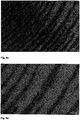
- Fig. 6 shows the localized growth of gold nanoparticles at 10 minutes UV irradiation using a mask with a circular pinhole (approximate diameter: 1 mm).
- a circular pinhole approximately 1 mm.
- no (at least not clear) further diffraction rings can be seen. This could eg at an unfavorable exposure time for the mask size.
- Fig. 9 shows the results using a slightly elliptical shadow mask and an exposure time of 10 minutes. Diffraction structures are visible and these were recorded with increasing magnification. Again, the relatively sharp demarcation of the individual rings becomes clear.
- Fig. 8 shows the results using a circular shadow mask and an exposure time of 30 minutes.
- the longer exposure time leads to a very strong growth in the exposed areas. This can be seen in particular at the overview shot (very bright ring structure).
- the area between the dark interior and the edge has been enlarged to a greatly enlarged area.
- the gold particles in the highest magnification ( Fig. 8d ) form a clearly recognizable edge.
- a purely qualitative determination of the size in the SEM leads to a radius of about 10 nm of the smaller (upper half of the picture) and about 17 nm of the larger particles (lower half of the picture).
- Fig. 7 shows the results using a further circular shadow mask and an exposure time of 30 minutes. Here again diffraction patterns can be seen. Again, the clearly demarcated ring structure is clearly visible.
Landscapes
- Chemical & Material Sciences (AREA)
- Materials Engineering (AREA)
- General Chemical & Material Sciences (AREA)
- Chemical Kinetics & Catalysis (AREA)
- Engineering & Computer Science (AREA)
- Mechanical Engineering (AREA)
- Metallurgy (AREA)
- Organic Chemistry (AREA)
- Optics & Photonics (AREA)
- Physics & Mathematics (AREA)
- Health & Medical Sciences (AREA)
- Toxicology (AREA)
- Manufacture Of Metal Powder And Suspensions Thereof (AREA)
- Other Surface Treatments For Metallic Materials (AREA)
Description
- Die vorliegende Erfindung betrifft Verfahren zur räumlich aufgelösten Vergrößerung und größenmäßigen Feineinstellung von Edelmetall-Nanopartikeln auf einer Substratoberfläche sowie die so hergestellten Nanopartikel-Anordnungen und nanostrukturierten Substratoberflächen und deren Verwendung.
- In den letzten Jahren haben Nanostrukturen, insbesondere geordnete Strukturen von Edelmetall-Nanopartikeln auf Substratoberflächen, großes Interesse für eine Vielzahl von Anwendungen auf unterschiedlichen Gebieten gefunden. Beispielsweise können Gold-Nanopartikel in biochemischen Sensoren eingesetzt (Dyckman und Bogatyrev (2007), Russian Chemical Reviews 76(2), 181-194) und als Ätzmasken zur Herstellung biomimetischer Ober- und Grenzflächen verwendet werden (Lohmüller et al. (2008), NANO LETTERS 8(5):1429-1433).
- Für viele dieser Anwendungen wäre es sehr wünschenswert, die Größe dieser Nanopartikel lokal und im Nanometermaßstab auf makroskopischen Substraten möglichst präzise einstellen zu können. Beispielsweise könnten an größere Nanopartikel mehr Linkermoleküle und damit auch mehr gewünschte Targetmoleküle gebunden werden und diese Kapazität zur Herstellung von Konzentrationsgradienten eines gegebenen Antigens auf einem Substrat genutzt werden. So könnten z.B. auf einfache Weise konzentrations-sensitive Biochips hergestellt werden. Auch für die obengenannte Verwendung als Ätzmasken wäre eine Feineinstellung der Partikelgröße mit hoher räumlicher Auflösung sehr vorteilhaft. Eine solche Feineinstellung würde beispielsweise die Herstellung komplexer nano-optischer Elemente wie Fresnel-Linsen und Zonenplatten ermöglichen. Geordnete Areale von Edelmetall-Nanopartikeln mit vorgegebenen Durchmessern könnten auch vorteilhaft in neuen Transistoren (Sato et al. (1997), American Institute of Physics 82(2), 696-702) oder für das Fluoreszenz-Quenching (Fan et al. (2003), PNAS, 100 (1), 6297-6301) verwendet werden.
Die Größe von Edelmetall-Nanopartikeln, insbesondere Gold-Nanopartikeln, kann grundsätzlich vor dem Aufbringen auf die Substratoberfläche, z.B. bei Verwendung von Metallkolloiden (Kimling et al. (2006), J. Phys. Chem. B., 110, 15700-15707), oder nach dem Aufbringen, z.B. durch stromlose Abscheidung unter Verwendung eines Reduktionsmittels (Hrapovic et al. (2003), Langmuir 19:3958-3965) eingestellt werden. Bei diesen im Stand der Technik beschriebenen Verfahren ist jedoch nur eine begrenzte Größeneinstellung möglich und vor allem keine räumlich aufgelöste Einstellung der Nanopartikelgröße.
In der deutschen PatentanmeldungDE 10 2007 017 032 und der entsprechenden internationalen AnmeldungPCT/EP2008/0071981 - Diese Verfahren sind jedoch noch nicht völlig zufriedenstellend und für alle Anwendungen geeignet, da es schwierig ist, mehrere Bereiche mit stark unterschiedlichen mittleren Durchmessern der Nanopartikel und hoher räumlicher Auflösung nebeneinander zu erzeugen.
- Eine Hauptaufgabe der vorliegenden Erfindung war somit die Bereitstellung von verbesserten Verfahren zur räumlich aufgelösten Vergrößerung und größenmäßigen Feineinstellung von Edelmetall-Nanopartikeln auf einer Substratoberfläche, mit denen auch sehr scharfe Partikelgrößengradienten oder Nanopartikelanordnungen, die mehrere Bereiche mit stark unterschiedlichen mittleren Durchmessern der Nanopartikel und hoher räumlicher Auflösung nebeneinander enthalten, auf einfache und effiziente Weise hergestellt werden können. Eine damit in Zusammenhang stehende Aufgabe war die Bereitstellung der entsprechenden Nanopartikelanordnungen und nanostrukturierten Substratoberflächen. Eine weitere Aufgabe war die Bereitstellung der erfindungsgemäß hergestellten Nanopartikelanordnungen und nanostrukturierten Substratoberflächen für verschiedene Verwendungen, die bisher aufgrund der nicht oder in nicht ausreichendem Umfang möglichen größenmäßigen Feinstellung von Edelmetall-Nanopartikeln auf einer Substratoberfläche für solche Edelmetall-Nanopartikelanordnungen nicht in Frage kamen.
- Erfindungsgemäß wurde nun festgestellt, dass die oben genannte Hauptaufgabe gelöst werden kann durch Bereitstellung des Verfahrens nach Anspruch 1, bei dem ein mit (vorzugsweise fixierten) Edelmetall-Nanopartikeln beschichtetes Substrat mit einer Edelmetallsalzlösung kontaktiert wird und durch UV-Bestrahlung von bestimmten vorgegebenen Bereichen eine lokalisierte und kontrollierte Vergrößerung der Nanopartikel in diesen Bereichen veranlasst wird. Die obengenannten weiteren Aufgaben werden durch Bereitstellung der Nanopartikelanordnungen und nanostrukturierten Substratoberflächen nach den Ansprüchen 13 und 14 sowie die Verwendung nach Anspruch 15 gelöst. Speziellere Ausführungsformen und andere Aspekte der vorliegenden Erfindung sind Gegenstand der weiteren Ansprüche.
- Die vorliegende Erfindung betrifft ein Verfahren zur räumlich aufgelösten Vergrößerung von Edelmetall-Nanopartikeln, die auf einem Substrat vorliegen, umfassend die folgenden Schritte:
- a) Bereitstellung eines mit Edelmetall-Nanopartikeln beschichteten Substrats,
- b) gegebenenfalls Funktionalisierung des Substrats mit einem Agens, welches die Haftung der Edelmetall-Nanopartikel an dem Substrat unterstützt,
- c) Kontaktierung des Substrats mit einer Edelmetallsalzlösung, wobei es sich bei der Edelmetallsalzlösung um eine wässrige Edelmetallsalzlösung handelt, der eine organische Verbindung zugesetzt wurde, welche bei UV-Bestrahlung organische Radikale bildet, die als Reduktionsmittel für die Edelmetallionen dienen,
- d) UV-Bestrahlung des Substrats in Kontakt mit der Edelmetallsalzlösung, wodurch eine Reduktion des Edelmetallsalzes und eine stromlose Abscheidung von elementarem Edelmetall auf den Edelmetall-Nanopartikeln und entsprechendes Wachstum der Edelmetall-Nanopartikel in den bestrahlten Bereichen des Substrats veranlasst wird,
- e) gegebenenfalls Verwendung einer Maske, um ein lokalisiertes Wachstum der Edelmetall-Nanopartikel in vorbestimmten Bereichen des Substrats zu veranlassen.
- Im Gegensatz zu diesem Verfahren wird in der obengenannten
DE 10 2007 017 032 A1 zwar ebenfalls eine Reduktion von Edelmetallionen durch Bestrahlung beschrieben, jenes Verfahren setzt jedoch das Vorhandensein eines Polymerfilms auf einer Substratoberfläche voraus. - In
EP 1 626 106 A2 wird ein getrockneter Metallkolloidfilm einer Laserbestrahlung unterworfen. Die Laserbestrahlung dient nicht zur Reduktion, sondern zur Entfernung von Molekülen des Dispersionsmittels, welche die feinen Metallpartikel zunächst getrennt halten. Nach deren Entfernung kommt es zur Aggregation und Bildung größerer Metallpartikel. -
EP 1760 527 A1 offenbart die Bestrahlung eines Polymerfilms auf einem Substrat zur Fixierung bzw. chemischen Modifizierung der Polymerkomponenten dieses Films. - Die Bereitstellung eines mit Edelmetall-Nanopartikeln beschichteten Substrats im obigen Schritt a) kann grundsätzlich mit allen im Stand der Technik bekannten Verfahren erfolgen. Beispielsweise kann eine Edelmetallkolloid-Schicht auf die Substratoberfläche aufgebracht werden (vgl. Hrapovic et al., oben). Eine andere, erfindungsgemäß bevorzugte Methode falls geordnete Nanopartikelstrukturen bereitgestellt werden sollen, besteht in der Erzeugung einer Edelmetall-Nanopartikelanordnung auf einem Substrat durch mizellare Nanolithographie, spezieller mizellare Block-copolymer-Nanolithographie (BCML) (siehe z.B.
EP 1 027 157 ). Bei der mizellaren Blockcopolymer-Nanolithographie wird eine mizellare Lösung eines Blockcopolymers auf ein Substrat abgeschieden, z.B. durch Tauchbeschichtung, und bildet unter geeigneten Bedingungen auf der Oberfläche eine geordnete Filmstruktur von chemisch unterschiedlichen Polymerdomänen, die unter anderem von Typ, Molekulargewicht und Konzentration des Blockcopolymers abhängt. Die Mizellen in der Lösung können mit anorganischen Salzen beladen werden, die nach der Abscheidung mit dem Polymerfilm zu anorganischen Nanopartikeln reduziert werden können. Zur Entfernung des Polymers wird in der Regel eine Plasmabehandlung, z.B. mit Wasserstoffplasma, durchgeführt. - Das erfindungsgemäß verwendete Substratmaterial ist grundsätzlich nicht besonders beschränkt und kann jegliches Material umfassen, solange es unter den Bedingungen des erfindungsgemäßen Verfahrens beständig ist und die stattfindenden Reaktionen nicht beeinträchtigt oder stört. Das Substrat kann beispielsweise aus Glas, SiO2, Silicium, Metallen (mit oder ohne passivierte(n) Oberflächen), Halbleitermaterialien, z.B. GaAs, GaP, GaInP, AlGaAs, (gegebenenfalls dotierten) Metalloxiden, z.B. ZnO, TiO2, Kohlenstoff (Graphit, Diamant), Polymeren etc. und Kompositmaterialien davon ausgewählt sein. Für einige Anwendungen sind transparente Substrate wie Glas oder ITO auf Glas bevorzugt.
- Das Edelmetall der Nanopartikel ist ebenfalls nicht besonders beschränkt und kann jedes im Stand der Technik für solche Nanopartikel bekannte Edelmetall oder Mischungen bzw. Komposite von mehreren Edelmetallen (Hybridpartikel) oder Mischungen eines Edelmetalls mit einem anderen Metall umfassen. Vorzugsweise ist das Edelmetall aus der Gruppe aus Au, Pt, Pd, Ag oder Mischungen/Komposite dieser Metalle ausgewählt und besonders bevorzugt handelt es sich um Gold.
- Die ursprünglichen Nanopartikel haben typischerweise Durchmesser im Bereich von 1 nm bis 100 nm, vorzugsweise von 4 nm to 30 nm. Die Interpartikeldistanzen können nach Wunsch über einen breiten Bereich variiert werden, beispielsweise in einem Bereich von 20 to 1000 nm, typischerweise im Bereich von 30 bis 250 nm.
- Zur Durchführung des erfindungsgemäßen Verfahrens ist es wichtig, dass eine gute Haftung der Edelmetall-Nanopartikel auf der Substratoberfläche gewährleistet ist. Zur Verbesserung der Haftung kann daher das Substrat erforderlichenfalls nach der Aufbringung der Nanopartikel, jedoch vor deren Vergrößerung, mit einem Agens behandelt werden, welches die Haftung der Nanopartikel unterstützt. Insbesondere bei Verwendung einer mit Gold-Nanopartikeln beschichteten Substratoberfläche aus Glas oder Siliciumdioxid, aber auch bei Si-, ZnO-, TiO2-, GaAs-Oberflächen und ähnlichen Oberflächen ist es bevorzugt, das Substrat mit einem Agens zu behandeln, welches die Haftung der Gold-Nanopartikel unterstützt. Dabei handelt es sich vorzugsweise um ein Silan, insbesondere aus der Gruppe ausgewählt, welche aus 3-Aminopropyltriethoxysilan (APS), 3-Mercaptopropyltriethoxysilan (MPS), N-[3-(Tri-methoxysilyl)propyl)ethylendiamin, 3-[2-(2-Aminoethylamino)-ethylamino]propyltrimethoxysilan, 3-Aminopropyldimethylmethoxysilan, 3-Aminopropyl)tris(trimethylsiloxy)silan und 3-Mercaptopropyltrimethoxysilan besteht.
- Bei der Edelmetallsalzlösung, die in Schritt c) mit der Substratoberfläche in Kontakt gebracht wird, handelt es sich um eine wässrige Metallsalzlösung, der eine organische Verbindung zugesetzt wurde, welche bei bzw. nach UV-Bestrahlung organische Radikale bildet, die als Reduktionsmittel für die Edelmetallionen dienen. Vorzugsweise ist diese organische Verbindung aus der Gruppe aus Aldehyden, Ketonen oder Alkoholen, insbesondere C1-C10-Alkoholen, ausgewählt. Besonders bevorzugt ist der C1-C10-Alkohol aus Methanol, Ethanol, Propanol, Butanol und Ethylenglycol ausgewählt. Der Anteil der organischen Verbindung kann zur Variation der Geschwindigkeit und des Ausmaßes der Reduktion vom Fachmann unschwer durch Routineversuche eingestellt werden. Typischerweise wird das Volumenverhältnis von wässriger Metallsalzlösung und organischer Verbindung in einem Bereich von 100:1 bis 1:2, bevorzugter 10:1 bis 1:1, z.B. 3:1 oder 1:1, liegen.
- In einer speziellen Ausführungsform ist die Edelmetallsalzlösung eine Goldsalzlösung, vorzugsweise eine HAuCl4-Lösung.
- Die Dauer der UV-Bestrahlung kann in Abhängigkeit von dem Ausmaß der gewünschten Nanopartikelvergrößerung und den jeweiligen Substratparametern variieren und eine geeignete Bestrahlungsdauer kann vom Fachmann unschwer mit Routineversuchen eingestellt werden. Typischerweise wird die UV-Bestrahlung für eine Dauer im Bereich von 1 bis 60 Minuten, vorzugsweise 1 bis 15 Minuten, und bei einer Wellenlänge im Bereich von 200 bis 600 nm, vorzugsweise 200 bis 400 nm, durchgeführt.
- Vorzugsweise wird das erfindungsgemäße Verfahren so durchgeführt, dass die Bedingungen der UV-Bestrahlung für mindestens zwei verschiedene Bereiche des Substrats variiert werden, sodass auf dem Substrat mindestens zwei verschiedene Bereiche mit unterschiedlichen mittleren Durchmessern der Edelmetall-Nanopartikel erzeugt werden. Diese Variation der Bedingungen der UV-Bestrahlung ist oder umfasst beispielsweise eine Variation der Bestrahlungsdauer.
- In einer bevorzugten Ausführungsform wird das erfindungsgemäße Verfahren unter Verwendung einer Maske (Schritt e)) durchgeführt, um ein lokalisiertes Wachstum der Edelmetall-Nanopartikel in vorbestimmten Bereichen des Substrats zu veranlassen.
- In einer spezielleren Ausführungsform weist die Maske Strukturen auf, die unter geeigneten Bestrahlungsbedingungen eine Beugung des eingestrahlten UV-Lichts erlauben, und das Verfahren wird unter solchen Bedingungen, insbesondere einer geeigneten Wellenlänge, durchgeführt, dass bei der Bestrahlung ein Diffraktionsmuster oder Helligkeitsmuster auf der Substratoberfläche gebildet wird und das Wachstum der Edelmetall-Nanopartikel selektiv in den stärker bestrahlten Bereichen des Diffraktionsmusters oder Helligkeitsmusters veranlasst wird.
- Diese Strukturen können beispielsweise eine oder mehrere Lochblenden mit einem kleinem Lochdurchmesser, vorzugsweise < 100 µm, bevorzugter < 10 µm, andere Beugungsgitter, Beugungskanten, periodische Muster oder Gradienten wie graduelle Graufilter umfassen. Die Lochblenden können beispielsweise eine kreisförmige, elliptische, rechteckige oder dreieckige Form aufweisen.
- Erfindungsgemäß ist es besonders bevorzugt, dass die Lochblende(n) einen kreisförmigen Durchmesser hat/haben, so dass bei der Bestrahlung ein Diffraktionsmuster von konzentrischen Ringen auf der Substratoberfläche gebildet wird und die erzeugten verschiedenen Bereiche mit unterschiedlichen mittleren Durchmessern der Edelmetall-Nanopartikel ebenfalls ein Muster konzentrischer Ringe bilden.
- Die vorliegende Erfindung betrifft auch ein Verfahren zur Herstellung einer nanostrukturierten Substratoberfläche, umfassend die Schritte a)-e) nach einem der Ansprüche 1-9 sowie ferner:
- f) Unterwerfen des Substrats mit der in den Schritten a)-e) nach einem der Ansprüche 1-9 entstandenen Edelmetall-Nanopartikelanordnung mindestens einem Ätzschritt, bei dem die Edelmetall-Nanopartikel als Ätzmaske wirken, womit durch selektive Ätzung in vorbestimmten Bereichen des Substrats unter Beibehaltung des Musters der Edelmetall-Nanopartikelanordnung eine gewünschte Reliefgestaltung der Substratoberfläche erzeugt wird. Bevorzugt wird dabei ein an das Substrat angepasstes Trockenätz-Verfahren verwendet. Im Falle von SiO2 z.B. ein "Reactive Ion" Ätzschritt unter Verwendung eines fluorhaltigen Ätzgases. Geeignete Verfahren sind beispielsweise in Lohmüller et al. (2008), NANO LETTERS, Bd. 8, Nr. 5, 1429-1433 beschrieben. Jedoch können auch andere im Stand der Technik bekannte und für das jeweilige Substrat geeignete Ätzverfahren angewandt werden.
Spezieller umfasst dieses Verfahren die Schritte a)-e) nach Anspruch 9 sowie ferner: - f) Unterwerfen des Substrats mit der in den Schritten a)-e) nach Anspruch 9 entstandenen Edelmetall-Nanopartikelanordnung, bei der verschiedene Bereiche mit unterschiedlichen mittleren Durchmessern der Edelmetall-Nanopartikel ein Muster konzentrischer Ringe bilden, mindestens einem Ätzschritt, bei dem die Edelmetall-Nanopartikel als Ätzmaske wirken, womit durch selektive Ätzung in vorbestimmten Bereichen des Substrats unter Beibehaltung des Musters von konzentrischen Kreisen eine Reliefgestaltung der Substratoberfläche erzeugt wird, die der einer Fresnel-Linse entspricht.
- Diese Anordnungen umfassen zwei oder mehr verschiedene Bereiche von Edelmetall-Nanopartikeln mit einem mittleren Durchmesser im Bereich von 5-200 nm, vorzugsweise 5-20 nm, und einer mittleren Beabstandung im Bereich von weniger als 1 µm, vorzugsweise von 30 bis 250 nm, wobei in den verschiedenen Bereichen jeweils Edelmetall-Nanopartikel mit einem vorgegebenen unterschiedlichen mittleren Durchmesser vorliegen und die verschiedenen Bereiche mit unterschiedlichen mittleren Durchmessern der Edelmetall-Nanopartikel ein oder mehrere geometrische(s) Muster bilden, welche(s) den durch Beugung von Strahlung an kreisförmigen, elliptischen, rechteckigen, dreieckigen Lochblenden, Kanten oder anderen periodisch angeordneten Mustern sowie Gradienten wie graduellen Graufiltern entstehenden Diffraktionsmustern oder Helligkeitsmustern entspricht/entsprechen.
- Besonders bevorzugt bilden die verschiedenen Bereiche ein Muster konzentrischer Ringe.
- Die mit den obigen erfindungsgemäßen Verfahren erhältlichen nanostrukturierten Substratoberflächen und Anordnungen von Edelmetall-Nanopartikeln auf einem Substrat bilden aufgrund der Möglichkeit zur Feineinstellung der Partikelgröße mit hoher räumlicher Auflösung und präziser Darstellung von geometrischen Mustern mit mehreren, scharf getrennten Bereichen unterschiedlicher Partikelgröße vorteilhafte Anwendungsmöglichkeiten auf unterschiedlichsten Fachgebieten.
- Dementsprechend betrifft ein weiterer Aspekt der vorliegenden Erfindung auch die Verwendung dieser nanostrukturierten Substratoberflächen und Anordnungen auf den Gebieten der Biochiptechnik, Bildgebungstechnik, Elektronik, Informationsverarbeitung, Spektroskopie, Sensortechnik, Optik, Lithographie.
- Eine solche Verwendung ist beispielweise deren Einsatz zur Herstellung optischer und elektronischer Vorrichtungen. In einer spezielleren Ausführungsform sind die Vorrichtungen aus der Gruppe ausgewählt, welche eine Maske, insbesondere Lithographie- oder Photomaske, einen Biochip, einen Sensor, eine optische Vorrichtung, insbesondere eine Fresnel-Linse, ein optisches Gitter, ein Mikrolinsenarray oder einen Transistor umfasst.
- Ein weiterer Gegenstand der Erfindung betrifft auch die Vorrichtungen selbst, welche solche nanostrukturierten Substratoberflächen oder Anordnungen umfassen. In einer spezielleren Ausführungsform handelt es sich bei diesen Vorrichtungen um eine Maske, insbesondere Lithographie- oder Photomaske, einen Biochip, einen Sensor, eine optische Vorrichtung, insbesondere eine Fresnel-Linse, ein optisches Gitter, ein Mikrolinsenarray oder einen Transistor.
-
-
Fig. 1 zeigt ein prinzipielles Schema zur Durchführung des erfindungsgemäßen Verfahrens mit einer durch mizellare Nanolithographie (BCML) bereitgestellten Gold-Nanopartikelanordnung. -
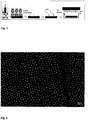
Fig. 2 zeigt eine Gold-Nanopartikelanordnung direkt nach einer BCML ohne weitere Vergrößerungsbehandlung der Partikel (Durchmesser der Nanopartikel: ca. 9 nm). -
Fig. 3 zeigt das Ergebnis einer stromlosen Abscheidung von Gold ohne vorherige Fixierung (Silanisierung) der Nanopartikel: Inhomogenes Partikelwachstum und Zerstörung der Ordnung -
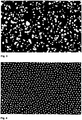
Fig. 4 zeigt Gold-Nanopartikel nach Silanisierung und 2,5 Minuten UV-Bestrahlung (Durchmesser der Nanopartikel: ca. 13 nm) . -
Fig. 5 zeigt Gold-Nanopartikel nach Silanisierung und 3 Minuten UV-Bestrahlung (Durchmesser der Nanopartikel: ca. 15 nm) . -
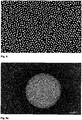
Fig. 6 zeigt das lokalisierte Wachstum von Gold-Nanopartikeln bei 10 Minuten UV-Bestrahlung unter Verwendung einer Maske mit einer kreisrunden Lochblende (Durchmesser ca. 1 mm);Fig. 6a : Gesamtansicht; 6b: Vergrößerung des hellen Innenraums mit stark gewachsenen Partikeln; 6c: Vergrößerung des Grenzbereichs von Innen- und Außenraum. -
Fig. 7 zeigt das lokalisierte Wachstum von Gold-Nanopartikeln bei 30 Minuten UV-Bestrahlung unter Verwendung einer Lochmaske mit wesentlich kleinerem, kreisrundem Lochblendendurchmesser als inFig. 6 : Entstehung eines Diffraktionsmusters mit konzentrischen Ringen; 7a: Gesamtansicht; 7b: vergrößerte Ringstruktur von 7a. -
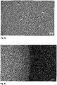
Fig. 8 zeigt das lokalisierte Wachstum von Gold-Nanopartikeln bei 30 Minuten UV-Bestrahlung unter Verwendung einer weiteren kreisrunden Lochmaske; 8a: Gesamtansicht; 8b-d; Vergrößerungen des Bereichs zwischen dem dunklen Innenraum und der Kante zum hellen Innenbereich mit stark vergrößerten Partikeln. -
Fig. 9 zeigt das lokalisierte Wachstum von Gold-Nanopartikeln mit erkennbaren Beugungsstrukturen bei 10 Minuten UV-Bestrahlung unter Verwendung einer leicht elliptischen Lochmaske; 9a: Gesamtansicht; 9b-d: Vergrößerungen eines Grenzbereichs. - Die folgenden Beispiele dienen zur näheren Erläuterung der vorliegenden Erfindung, ohne diese jedoch darauf zu beschränken.
- Das zu belichtende Sample bestehend aus SiO2, dessen Oberfläche Gold-Nanopartikel mit einem mittleren Durchmesser von ca. 9 nm aufwies (
Fig. 2 ), wurde mit Silan behandelt (Gasphasenabscheidung von 3-Aminopropyltriethoxysilan (APS): Sample + 30 uL APS (in separater Schale) im Exsikkator für 30 Minuten bei 0,3 mbar. Danach 1 h bei 80°C im Ofen.) und zur Belichtung in ein kleines Gefäß gegeben. In das Gefäß wurde eine 1:1 Mischung von 0,25%iger Goldsalzlösung (HAuCl4) und Ethanol gegeben. Die Menge der Lösung wurde dabei so bemessen, dass das Sample von einem ca. 1 mm hohen Flüssigkeitsfilm bedeckt war. Anschließend wurde ohne Maske mit UV-Licht (kommerzielle UV-Lampe, Wellenlänge: 410 nm) bestrahlt. Belichtungszeiten von 2' 30" ergaben Partikeldurchmesser von ca. 13 nm (Fig. 4 ); Belichtungszeiten von 3' Durchmesser von ca. 15 nm (Fig. 5 ). - Fresnelbeugung tritt auf, wenn folgende Ungleichung erfüllt ist:

- Diese Bedingung ist bei allen folgenden Experimenten erfüllt, es handelt sich also immer um Fresnelbeugung und nicht um Fraunhoferbeugung.
- Das Beugungsintegral lässt sich nach Anwendung der Fresnelnäherung nicht analytisch lösen, sondern nur numerisch. Das entstehende Beugungsmuster reagiert dabei extrem empfindlich auf kleinste Änderungen des Abstandes oder des Blendendurchmessers. Da eine Realisierung von konstanten Bedingungen (völlig planares Sample, völlig planare Maske, keine "Wellenbildung" der Lösung,) nur mit größerem Aufwand zu realisieren ist, wurde für die nachfolgenden Versuchsanordnungen und Bilder ein einfacherer (qualitativer) Ansatz gewählt.
- Das zu belichtende Sample wurde in ein kleines Gefäß gegeben. In das Gefäß wurde eine Lösung aus 1,5 ml 0,25% Goldsalzlösung (HAuCl4) und 0,5 ml Ethanol gegeben. Die Menge der Lösung war dabei so bemessen, dass das Sample von einem ca. 1 mm hohen Flüssigkeitsfilm bedeckt ist. Als Maske wurde Aluminiumfolie, die mit Löchern zwischen 0,6 mm und 2 mm perforiert ist, verwendet. Diese Maske wurde ca. 1,1 mm oberhalb des Samples angebracht. Anschließend wurde mit UV-Licht 10 oder 30 Minuten lang belichtet.
-
Fig. 6 zeigt das lokalisierte Wachstum von Gold-Nanopartikeln bei 10 Minuten UV-Bestrahlung unter Verwendung einer Maske mit einer kreisrunden Lochblende (ungefährer Durchmesser: 1 mm). Hier sieht man sehr schön den helleren Innenraum, der klar vom Außenraum mit weniger stark gewachsenen Partikeln abgegrenzt ist. Hier sind jedoch keine (zumindest keine deutlichen) weiteren Beugungsringe zu erkennen. Dies könnte z.B. an einer für die Maskengröße ungünstigen Belichtungszeit gelegen haben. -
Fig. 9 zeigt die Ergebnisse bei Verwendung einer leicht elliptischen Lochmaske und einer Belichtungszeit von 10 Minuten. Beugungsstrukturen sind erkennbar und diese wurden mit zunehmender Vergrößerung aufgenommen. Auch dabei wird wieder die relativ scharfe Abgrenzung der einzelnen Ringe deutlich. -
Fig. 8 zeigt die Ergebnisse bei Verwendung einer kreisrunden Lochmaske und einer Belichtungszeit von 30 Minuten. Die längere Belichtungszeit führt zu einem sehr starken Wachstum an den belichteten Stellen. Dies sieht man insbesondere an der Übersichtsaufnahme (sehr helle Ringstruktur). Vergrößert wurde der Bereich zwischen dem dunklen Innenraum und der Kante zum stark vergrößerten Bereich. Die Goldpartikel in der höchsten Vergrößerung (Fig. 8d ) bilden eine klar erkennbare Kante. Eine rein qualitative Größenbestimmung im SEM führt zu m Radius von ca. 10 nm der kleineren (obere Bildhälfte) und ca. 17 nm der größeren Partikel (untere Bildhälfte). -
Fig. 7 zeigt die Ergebnisse bei Verwendung einer weiteren kreisrunden Lochmaske und einer Belichtungszeit von 30 Minuten. Hier sind wieder Beugungsmuster zu erkennen. Auch ist wiederum die deutlich abgegrenzte Ringstruktur gut zu erkennen.
Claims (17)
- Verfahren zur räumlich aufgelösten Vergrößerung von Edelmetall-Nanopartikeln, die auf einem Substrat vorliegen, umfassend die folgenden Schritte:a) Bereitstellung eines mit Edelmetall-Nanopartikeln beschichteten Substrats,b) gegebenenfalls Funktionalisierung des Substrats mit einem Agens, welches die Haftung der Edelmetall-Nanopartikel an dem Substrat unterstützt,c) Kontaktierung des Substrats mit einer Edelmetallsalzlösung, wobei es sich bei der Edelmetallsalzlösung um eine wässrige Edelmetallsalzlösung handelt, der eine organische Verbindung zugesetzt wurde, welche bei UV-Bestrahlung organische Radikale bildet, die als Reduktionsmittel für die Edelmetallionen dienen,d) UV-Bestrahlung des Substrats in Kontakt mit der Edelmetallsalzlösung, wodurch eine Reduktion des Edelmetallsalzes und eine stromlose Abscheidung von elementarem Edelmetall auf den Edelmetall-Nanopartikeln und entsprechendes Wachstum der Edelmetall-Nanopartikel in den bestrahlten Bereichen des Substrats veranlasst wird,e) gegebenenfalls Verwendung einer Maske, um ein lokalisiertes Wachstum der Edelmetall-Nanopartikel in vorbestimmten Bereichen des Substrats zu veranlassen.
- Verfahren nach Anspruch 1, dadurch gekennzeichnet, dass das Edelmetall aus der Gruppe aus Gold, Silber, Palladium und Platin ausgewählt ist.
- Verfahren nach Anspruch 1 oder 2, dadurch gekennzeichnet, dass das mit Edelmetall-Nanopartikeln beschichtete Substrat durch mizellare Blockcopolymer-Lithographie (BCML) oder durch Aufbringung einer Edelmetallkolloid-Schicht auf die Substratoberfläche bereitgestellt wird.
- Verfahren nach irgendeinem der Ansprüche 1-3, dadurch gekennzeichnet, dass das Agens, welches die Haftung von Edelmetall-Nanopartikeln an dem Substrat unterstützt, ein Silan ist, insbesondere aus der Gruppe ausgewählt, welche aus 3-Aminopropyltriethoxysilan (APS), 3-Mercaptopropyltriethoxysilan (MPS), N-[3-(Trimethoxysilyl)propyl)ethylendiamin, 3-[2-(2-Aminoethylamino)ethylamino]propyltrimethoxysilan, 3-Aminopropyldimethylmethoxysilan, 3-Aminopropyl)-tris(trimethylsiloxy)silan und 3-Mercaptopropyltrimethoxysilan besteht.
- Verfahren nach irgendeinem der Ansprüche 1-4, dadurch gekennzeichnet, dass es sich bei der organischen Verbindung, die der Edelmetallsalzlösung zugesetzt wurde, um einen Aldehyd, ein Keton oder einen Alkohol, vorzugsweise einen C1-C10-Alkohol, handelt.
- Verfahren nach irgendeinem der Ansprüche 1-5, dadurch gekennzeichnet, dass die Bedingungen der UV-Bestrahlung für mindestens zwei verschiedene Bereiche des Substrats variiert werden, sodass auf dem Substrat mindestens zwei verschiedene Bereiche mit unterschiedlichen mittleren Durchmessern der Edelmetall-Nanopartikel erzeugt werden.
- Verfahren nach irgendeinem der Ansprüche 1-6, dadurch gekennzeichnet, dass Schritt e) unter Verwendung einer Maske, die eine oder mehrere Lochblenden mit einem Lochdurchmesser < 10 µm, andere Beugungsgitter, Beugungskanten oder Gradienten wie graduelle Graufilter enthält, und unter solchen Bedingungen durchgeführt wird, dass bei der Bestrahlung ein Diffraktionsmuster oder Helligkeitsmuster auf der Substratoberfläche gebildet wird und das Wachstum der Edelmetall-Nanopartikel selektiv in den stärker bestrahlten Bereichen des Diffraktionsmusters oder Helligkeitsmusters veranlasst wird.
- Verfahren nach Anspruch 7, dadurch gekennzeichnet, dass Schritt e) unter Verwendung einer Maske, die eine oder mehrere Lochblenden mit einem Lochdurchmesser < 10 µm von kreisförmiger, elliptischer, rechteckiger oder dreieckiger Form enthält, durchgeführt wird.
- Verfahren nach Anspruch 8, dadurch gekennzeichnet, dass die Lochblende(n) einen kreisförmigen Durchmesser hat/haben, so dass bei der Bestrahlung ein Diffraktionsmuster von konzentrischen Ringen auf der Substratoberfläche gebildet wird und die erzeugten verschiedenen Bereiche mit unterschiedlichen mittleren Durchmessern der Edelmetall-Nanopartikel ebenfalls ein Muster konzentrischer Ringe bilden.
- Verfahren zur Herstellung einer nanostrukturierten Substratoberfläche, umfassend die Schritte a)-e) nach einem der Ansprüche 1-9 sowie ferner:f) Unterwerfen des Substrats mit der in den Schritten a)-e) nach einem der Ansprüche 1-9 entstandenen Edelmetall-Nanopartikelanordnung mindestens einem Ätzschritt, bei dem die Edelmetall-Nanopartikel als Ätzmaske wirken, womit durch selektive Ätzung in vorbestimmten Bereichen des Substrats unter Beibehaltung des Musters der Edelmetall-Nanopartikelanordnung eine gewünschte Reliefgestaltung der Substratoberfläche erzeugt wird.
- Verfahren zur Herstellung einer nanostrukturierten Substratoberfläche nach Anspruch 10, umfassend die Schritte a)-e) nach einem der Ansprüche 7-8 sowie ferner:f) Unterwerfen des Substrats mit der in den Schritten a)-e) nach einem der Ansprüche 7-8 entstandenen Edelmetall-Nanopartikelanordnung mindestens einem Ätzschritt, bei dem die Edelmetall-Nanopartikel als Ätzmaske wirken, womit durch selektive Ätzung in vorbestimmten Bereichen des Substrats unter Beibehaltung des Musters der Edelmetall-Nanopartikelanordnung eine gewünschte Reliefgestaltung der Substratoberfläche erzeugt wird.
- Verfahren zur Herstellung einer nanostrukturierten Substratoberfläche nach Anspruch 10, umfassend die Schritte a)-e) nach Anspruch 9 sowie ferner:f) Unterwerfen des Substrats mit der in den Schritten a)-e) nach Anspruch 9 entstandenen Edelmetall-Nanopartikelanordnung, bei der verschiedene Bereiche mit unterschiedlichen mittleren Durchmessern der Edelmetall-Nanopartikel ein Muster konzentrischer Ringe bilden, mindestens einem Ätzschritt, bei dem die Edelmetall-Nanopartikel als Ätzmaske wirken, womit durch selektive Ätzung in vorbestimmten Bereichen des Substrats unter Beibehaltung des Musters von konzentrischen Kreisen eine Reliefgestaltung der Substratoberfläche erzeugt wird, die der einer Fresnel-Linse entspricht.
- Nanostrukturierte Substratoberfläche, erhältlich mit dem Verfahren nach Anspruch 11 oder 12.
- Anordnung von Edelmetall-Nanopartikeln, insbesondere Gold-, Silber-, Palladium- und Platin-Nanopartikel oder Hybridpartikel davon, auf einem Substrat, erhältlich nach einem der Ansprüche 7 bis 9, wobei die Anordnung zwei oder mehr verschiedene Bereiche von Edelmetall-Nanopartikeln mit einem mittleren Durchmesser im Bereich von 5-200 nm und einer mittleren Beabstandung im Bereich von weniger als 1 µm umfasst, wobei in den verschiedenen Bereichen jeweils Edelmetall-Nanopartikel mit einem vorgegebenen unterschiedlichen mittleren Durchmesser vorliegen und dass die verschiedenen Bereiche mit unterschiedlichen mittleren Durchmessern der Edelmetall-Nanopartikel ein oder mehrere geometrische(s) Muster bilden, welche(s) den durch Beugung von Strahlung an kreisförmigen, elliptischen, rechteckigen, dreieckigen Blenden, Kanten oder anderen periodisch angeordneten Mustern sowie Gradienten wie graduellen Graufiltern entstehenden Diffraktionsmustern oder Helligkeitsmustern entspricht/entsprechen.
- Verwendung der nanostrukturierten Substratoberfläche nach Anspruch 13 oder der Anordnung nach Anspruch 14 auf den Gebieten der Biochiptechnik, Bildgebungstechnik, Elektronik, Informationsverarbeitung, Spektroskopie, Sensortechnik, Optik, Lithographie, insbesondere zur Herstellung einer Lithographie- oder Photomaske, eines Biochips, eines Sensors, einer optischen Vorrichtung, insbesondere einer Fresnel-Linse, eines optischen Gitters, eines Mikrolinsenarrays oder eines Transistors.
- Vorrichtung, umfassend die nanostrukturierte Substratoberfläche nach Anspruch 13 oder die Anordnung nach Anspruch 14.
- Vorrichtung nach Anspruch 16, bei der es sich um eine Maske, insbesondere Lithographie- oder Photomaske, einen Biochip, einen Sensor, eine optische Vorrichtung, insbesondere eine Fresnel-Linse, ein optisches Gitter, ein Mikrolinsenarray oder einen Transistor handelt.
Applications Claiming Priority (2)
| Application Number | Priority Date | Filing Date | Title |
|---|---|---|---|
| DE102009053406A DE102009053406A1 (de) | 2009-11-16 | 2009-11-16 | Verfahren zur räumlich aufgelösten Vergrößerung von Nanopartikeln auf einer Substratoberfläche |
| PCT/EP2010/006938 WO2011057816A2 (de) | 2009-11-16 | 2010-11-15 | Verfahren zur räumlich aufgelösten vergrösserung von nanopartikeln auf einer substratoberfläche |
Publications (2)
| Publication Number | Publication Date |
|---|---|
| EP2501842A2 EP2501842A2 (de) | 2012-09-26 |
| EP2501842B1 true EP2501842B1 (de) | 2018-08-29 |
Family
ID=43877657
Family Applications (1)
| Application Number | Title | Priority Date | Filing Date |
|---|---|---|---|
| EP10778575.0A Active EP2501842B1 (de) | 2009-11-16 | 2010-11-15 | Verfahren zur räumlich aufgelösten vergrösserung von nanopartikeln auf einer substratoberfläche |
Country Status (4)
| Country | Link |
|---|---|
| US (1) | US9169566B2 (de) |
| EP (1) | EP2501842B1 (de) |
| DE (1) | DE102009053406A1 (de) |
| WO (1) | WO2011057816A2 (de) |
Families Citing this family (6)
| Publication number | Priority date | Publication date | Assignee | Title |
|---|---|---|---|---|
| DE102010023490A1 (de) | 2010-06-11 | 2011-12-15 | MAX-PLANCK-Gesellschaft zur Förderung der Wissenschaften e.V. | Dreidimensionale metallbedeckte Nanostrukturen auf Substratoberflächen,Verfahren zu deren Erzeugung sowie deren Verwendung |
| WO2015053828A2 (en) | 2013-06-15 | 2015-04-16 | Brookhaven Science Associates, Llc | Formation of antireflective surfaces |
| US10290507B2 (en) | 2013-06-15 | 2019-05-14 | Brookhaven Science Associates, Llc | Formation of antireflective surfaces |
| DE102013111785B4 (de) * | 2013-10-25 | 2025-12-24 | Pictiva Displays International Limited | Verfahren zum Herstellen eines optoelektronischen Bauelementes |
| US11135649B2 (en) | 2018-02-27 | 2021-10-05 | Arizona Board Of Regents On Behalf Of Arizona State University | Direct metal printing with stereolithography |
| US12502823B2 (en) * | 2022-01-13 | 2025-12-23 | Arizona Board Of Regents On Behalf Of Arizona State University | Color image printing by polymer-assisted photochemical deposition |
Family Cites Families (6)
| Publication number | Priority date | Publication date | Assignee | Title |
|---|---|---|---|---|
| JP2004500226A (ja) | 1997-10-29 | 2004-01-08 | ウニベルジテート ウルム | ナノ構造物 |
| JP2006038999A (ja) | 2004-07-23 | 2006-02-09 | Sumitomo Electric Ind Ltd | レーザ照射を用いた導電性回路形成方法と導電性回路 |
| US8361553B2 (en) * | 2004-07-30 | 2013-01-29 | Kimberly-Clark Worldwide, Inc. | Methods and compositions for metal nanoparticle treated surfaces |
| EP1760527B1 (de) * | 2005-09-05 | 2012-06-06 | DWI an der RWTH Aachen e.V. | Photochemische Methode für die Produktion von oberflächenverzierten Substraten im Nanometerbereich |
| DE102007014538A1 (de) | 2007-03-27 | 2008-10-02 | Carl Zeiss Ag | Verfahren zur Erzeugung einer Antireflexionsoberfläche auf einem optischen Element sowie optische Elemente mit einer Antireflexionsoberfläche |
| DE102007017032B4 (de) | 2007-04-11 | 2011-09-22 | MAX-PLANCK-Gesellschaft zur Förderung der Wissenschaften e.V. | Verfahren zur Herstellung von flächigen Größen- oder Abstandsvariationen in Mustern von Nanostrukturen auf Oberflächen |
-
2009
- 2009-11-16 DE DE102009053406A patent/DE102009053406A1/de not_active Ceased
-
2010
- 2010-11-15 EP EP10778575.0A patent/EP2501842B1/de active Active
- 2010-11-15 WO PCT/EP2010/006938 patent/WO2011057816A2/de not_active Ceased
- 2010-11-15 US US13/510,107 patent/US9169566B2/en active Active
Also Published As
| Publication number | Publication date |
|---|---|
| US20120244322A1 (en) | 2012-09-27 |
| EP2501842A2 (de) | 2012-09-26 |
| WO2011057816A3 (de) | 2011-08-11 |
| WO2011057816A2 (de) | 2011-05-19 |
| US9169566B2 (en) | 2015-10-27 |
| DE102009053406A1 (de) | 2011-05-19 |
Similar Documents
| Publication | Publication Date | Title |
|---|---|---|
| EP2295617B1 (de) | Verfahren zur Herstellung von flächigen Größen- oder Abstandsvariationen in Mustern von Nanostrukturen auf Oberflächen | |
| EP2501842B1 (de) | Verfahren zur räumlich aufgelösten vergrösserung von nanopartikeln auf einer substratoberfläche | |
| DE602004005652T2 (de) | Mikrostrukturkörper für die Raman-Spektroskopie und Verfahren zu dessen Herstellung | |
| CN108844943B (zh) | Sers单元及其制备方法与应用 | |
| EP2931937B1 (de) | Verfahren zur herstellung von metall-nanopartikel-arrays | |
| DE102015004114B4 (de) | Oberflächenverstärkendes plasmonisches Substrat | |
| DE112011100503T5 (de) | Ein verfahren und eine vorrichtung zur vorbereitung eines substrats für eine molekulare detektion | |
| KR102169831B1 (ko) | 표면증강라만산란용 기판 및 이의 제조방법 | |
| Kim et al. | Reshaping nanocrystals for tunable plasmonic substrates | |
| DE102015115004A1 (de) | Verfahren zur Herstellung von strukturierten Oberflächen | |
| DE60123921T2 (de) | Verfahren zur Herstellung von ultrafeinen Metallchalkogenidteilchen | |
| AT519922A1 (de) | SERS-Substrat | |
| DE102012200454A1 (de) | Verfahren zur Herstellung eines reflektiven optischen Elements und reflektives optisches Element | |
| WO2010133217A1 (de) | Vorrichtung und verfahren zur metallisierung von rastersondenspitzen | |
| DE112023002319T5 (de) | Immobilisierter zweidimensionaler kolloidaler kristall und verfahren zur herstellung desselben | |
| DE102018106707A1 (de) | Verfahren zur Herstellung und Verwendung eines Substrats mit einer funktionalisierten Oberfläche | |
| DE112005002689T5 (de) | Mit Teilchen laminiertes Substrat und Verfahren zu dessen Herstellung | |
| DE102016118440B4 (de) | Aktivierte 3-D-Nanooberfläche, Verfahren zu ihrer Herstellung und ihre Verwendung | |
| DE102005011345A1 (de) | Verfahren zum Herstellen einer Nanostruktur auf einem Substrat | |
| DE102016208987A1 (de) | Optisches Element und EUV-Lithographiesystem | |
| DE102008016552B4 (de) | Optischer Sensor | |
| CH703612B1 (de) | Verfahren zur Beschichtung von hydrophilen Festkörpern mit einer Goldschicht mit ausgedehnter Oberfläche sowie ein mit einer Goldschicht mit ausgedehnter Oberfläche beschichteter hydrophiler Festkörper. | |
| DE102009023796B4 (de) | Vorrichtung und Verfahren zur Metallisierung von Rastersondenspitzen | |
| EP4421541A1 (de) | Strukturiertes halbleiterbauteil und verfahren zur herstellung eines strukturierten halbleiterbauteils | |
| DE102020212940A1 (de) | Strukturierte Schichtanordnung und Verfahren zum Herstellen einer derartigen Schichtanordnung |
Legal Events
| Date | Code | Title | Description |
|---|---|---|---|
| PUAI | Public reference made under article 153(3) epc to a published international application that has entered the european phase |
Free format text: ORIGINAL CODE: 0009012 |
|
| 17P | Request for examination filed |
Effective date: 20120613 |
|
| AK | Designated contracting states |
Kind code of ref document: A2 Designated state(s): AL AT BE BG CH CY CZ DE DK EE ES FI FR GB GR HR HU IE IS IT LI LT LU LV MC MK MT NL NO PL PT RO RS SE SI SK SM TR |
|
| DAX | Request for extension of the european patent (deleted) | ||
| STAA | Information on the status of an ep patent application or granted ep patent |
Free format text: STATUS: EXAMINATION IS IN PROGRESS |
|
| 17Q | First examination report despatched |
Effective date: 20170807 |
|
| RIC1 | Information provided on ipc code assigned before grant |
Ipc: C23C 18/16 20060101AFI20180329BHEP Ipc: C23C 18/44 20060101ALI20180329BHEP |
|
| GRAP | Despatch of communication of intention to grant a patent |
Free format text: ORIGINAL CODE: EPIDOSNIGR1 |
|
| STAA | Information on the status of an ep patent application or granted ep patent |
Free format text: STATUS: GRANT OF PATENT IS INTENDED |
|
| INTG | Intention to grant announced |
Effective date: 20180511 |
|
| GRAS | Grant fee paid |
Free format text: ORIGINAL CODE: EPIDOSNIGR3 |
|
| GRAA | (expected) grant |
Free format text: ORIGINAL CODE: 0009210 |
|
| STAA | Information on the status of an ep patent application or granted ep patent |
Free format text: STATUS: THE PATENT HAS BEEN GRANTED |
|
| AK | Designated contracting states |
Kind code of ref document: B1 Designated state(s): AL AT BE BG CH CY CZ DE DK EE ES FI FR GB GR HR HU IE IS IT LI LT LU LV MC MK MT NL NO PL PT RO RS SE SI SK SM TR |
|
| REG | Reference to a national code |
Ref country code: GB Ref legal event code: FG4D Free format text: NOT ENGLISH |
|
| RIN1 | Information on inventor provided before grant (corrected) |
Inventor name: PACHOLSKI, CLAUDIA Inventor name: SPATZ, JOACHIM P. Inventor name: MORHARD, CHRISTOPH |
|
| REG | Reference to a national code |
Ref country code: CH Ref legal event code: EP |
|
| REG | Reference to a national code |
Ref country code: CH Ref legal event code: NV Representative=s name: KASCHE AND PARTNER AG, CH |
|
| REG | Reference to a national code |
Ref country code: AT Ref legal event code: REF Ref document number: 1035222 Country of ref document: AT Kind code of ref document: T Effective date: 20180915 |
|
| REG | Reference to a national code |
Ref country code: IE Ref legal event code: FG4D Free format text: LANGUAGE OF EP DOCUMENT: GERMAN |
|
| REG | Reference to a national code |
Ref country code: DE Ref legal event code: R096 Ref document number: 502010015314 Country of ref document: DE |
|
| REG | Reference to a national code |
Ref country code: NL Ref legal event code: FP |
|
| REG | Reference to a national code |
Ref country code: LT Ref legal event code: MG4D |
|
| PG25 | Lapsed in a contracting state [announced via postgrant information from national office to epo] |
Ref country code: SE Free format text: LAPSE BECAUSE OF FAILURE TO SUBMIT A TRANSLATION OF THE DESCRIPTION OR TO PAY THE FEE WITHIN THE PRESCRIBED TIME-LIMIT Effective date: 20180829 Ref country code: BG Free format text: LAPSE BECAUSE OF FAILURE TO SUBMIT A TRANSLATION OF THE DESCRIPTION OR TO PAY THE FEE WITHIN THE PRESCRIBED TIME-LIMIT Effective date: 20181129 Ref country code: IS Free format text: LAPSE BECAUSE OF FAILURE TO SUBMIT A TRANSLATION OF THE DESCRIPTION OR TO PAY THE FEE WITHIN THE PRESCRIBED TIME-LIMIT Effective date: 20181229 Ref country code: NO Free format text: LAPSE BECAUSE OF FAILURE TO SUBMIT A TRANSLATION OF THE DESCRIPTION OR TO PAY THE FEE WITHIN THE PRESCRIBED TIME-LIMIT Effective date: 20181129 Ref country code: LT Free format text: LAPSE BECAUSE OF FAILURE TO SUBMIT A TRANSLATION OF THE DESCRIPTION OR TO PAY THE FEE WITHIN THE PRESCRIBED TIME-LIMIT Effective date: 20180829 Ref country code: RS Free format text: LAPSE BECAUSE OF FAILURE TO SUBMIT A TRANSLATION OF THE DESCRIPTION OR TO PAY THE FEE WITHIN THE PRESCRIBED TIME-LIMIT Effective date: 20180829 Ref country code: FI Free format text: LAPSE BECAUSE OF FAILURE TO SUBMIT A TRANSLATION OF THE DESCRIPTION OR TO PAY THE FEE WITHIN THE PRESCRIBED TIME-LIMIT Effective date: 20180829 Ref country code: GR Free format text: LAPSE BECAUSE OF FAILURE TO SUBMIT A TRANSLATION OF THE DESCRIPTION OR TO PAY THE FEE WITHIN THE PRESCRIBED TIME-LIMIT Effective date: 20181130 |
|
| PG25 | Lapsed in a contracting state [announced via postgrant information from national office to epo] |
Ref country code: LV Free format text: LAPSE BECAUSE OF FAILURE TO SUBMIT A TRANSLATION OF THE DESCRIPTION OR TO PAY THE FEE WITHIN THE PRESCRIBED TIME-LIMIT Effective date: 20180829 Ref country code: AL Free format text: LAPSE BECAUSE OF FAILURE TO SUBMIT A TRANSLATION OF THE DESCRIPTION OR TO PAY THE FEE WITHIN THE PRESCRIBED TIME-LIMIT Effective date: 20180829 Ref country code: HR Free format text: LAPSE BECAUSE OF FAILURE TO SUBMIT A TRANSLATION OF THE DESCRIPTION OR TO PAY THE FEE WITHIN THE PRESCRIBED TIME-LIMIT Effective date: 20180829 |
|
| PG25 | Lapsed in a contracting state [announced via postgrant information from national office to epo] |
Ref country code: IT Free format text: LAPSE BECAUSE OF FAILURE TO SUBMIT A TRANSLATION OF THE DESCRIPTION OR TO PAY THE FEE WITHIN THE PRESCRIBED TIME-LIMIT Effective date: 20180829 Ref country code: EE Free format text: LAPSE BECAUSE OF FAILURE TO SUBMIT A TRANSLATION OF THE DESCRIPTION OR TO PAY THE FEE WITHIN THE PRESCRIBED TIME-LIMIT Effective date: 20180829 Ref country code: CZ Free format text: LAPSE BECAUSE OF FAILURE TO SUBMIT A TRANSLATION OF THE DESCRIPTION OR TO PAY THE FEE WITHIN THE PRESCRIBED TIME-LIMIT Effective date: 20180829 Ref country code: RO Free format text: LAPSE BECAUSE OF FAILURE TO SUBMIT A TRANSLATION OF THE DESCRIPTION OR TO PAY THE FEE WITHIN THE PRESCRIBED TIME-LIMIT Effective date: 20180829 Ref country code: ES Free format text: LAPSE BECAUSE OF FAILURE TO SUBMIT A TRANSLATION OF THE DESCRIPTION OR TO PAY THE FEE WITHIN THE PRESCRIBED TIME-LIMIT Effective date: 20180829 Ref country code: PL Free format text: LAPSE BECAUSE OF FAILURE TO SUBMIT A TRANSLATION OF THE DESCRIPTION OR TO PAY THE FEE WITHIN THE PRESCRIBED TIME-LIMIT Effective date: 20180829 |
|
| PG25 | Lapsed in a contracting state [announced via postgrant information from national office to epo] |
Ref country code: SK Free format text: LAPSE BECAUSE OF FAILURE TO SUBMIT A TRANSLATION OF THE DESCRIPTION OR TO PAY THE FEE WITHIN THE PRESCRIBED TIME-LIMIT Effective date: 20180829 Ref country code: SM Free format text: LAPSE BECAUSE OF FAILURE TO SUBMIT A TRANSLATION OF THE DESCRIPTION OR TO PAY THE FEE WITHIN THE PRESCRIBED TIME-LIMIT Effective date: 20180829 Ref country code: DK Free format text: LAPSE BECAUSE OF FAILURE TO SUBMIT A TRANSLATION OF THE DESCRIPTION OR TO PAY THE FEE WITHIN THE PRESCRIBED TIME-LIMIT Effective date: 20180829 |
|
| REG | Reference to a national code |
Ref country code: DE Ref legal event code: R097 Ref document number: 502010015314 Country of ref document: DE |
|
| PLBE | No opposition filed within time limit |
Free format text: ORIGINAL CODE: 0009261 |
|
| STAA | Information on the status of an ep patent application or granted ep patent |
Free format text: STATUS: NO OPPOSITION FILED WITHIN TIME LIMIT |
|
| PG25 | Lapsed in a contracting state [announced via postgrant information from national office to epo] |
Ref country code: LU Free format text: LAPSE BECAUSE OF NON-PAYMENT OF DUE FEES Effective date: 20181115 Ref country code: MC Free format text: LAPSE BECAUSE OF FAILURE TO SUBMIT A TRANSLATION OF THE DESCRIPTION OR TO PAY THE FEE WITHIN THE PRESCRIBED TIME-LIMIT Effective date: 20180829 |
|
| 26N | No opposition filed |
Effective date: 20190531 |
|
| REG | Reference to a national code |
Ref country code: BE Ref legal event code: MM Effective date: 20181130 |
|
| REG | Reference to a national code |
Ref country code: IE Ref legal event code: MM4A |
|
| PG25 | Lapsed in a contracting state [announced via postgrant information from national office to epo] |
Ref country code: SI Free format text: LAPSE BECAUSE OF FAILURE TO SUBMIT A TRANSLATION OF THE DESCRIPTION OR TO PAY THE FEE WITHIN THE PRESCRIBED TIME-LIMIT Effective date: 20180829 |
|
| PG25 | Lapsed in a contracting state [announced via postgrant information from national office to epo] |
Ref country code: IE Free format text: LAPSE BECAUSE OF NON-PAYMENT OF DUE FEES Effective date: 20181115 |
|
| PG25 | Lapsed in a contracting state [announced via postgrant information from national office to epo] |
Ref country code: BE Free format text: LAPSE BECAUSE OF NON-PAYMENT OF DUE FEES Effective date: 20181130 |
|
| REG | Reference to a national code |
Ref country code: AT Ref legal event code: MM01 Ref document number: 1035222 Country of ref document: AT Kind code of ref document: T Effective date: 20181115 |
|
| PG25 | Lapsed in a contracting state [announced via postgrant information from national office to epo] |
Ref country code: AT Free format text: LAPSE BECAUSE OF NON-PAYMENT OF DUE FEES Effective date: 20181115 Ref country code: MT Free format text: LAPSE BECAUSE OF FAILURE TO SUBMIT A TRANSLATION OF THE DESCRIPTION OR TO PAY THE FEE WITHIN THE PRESCRIBED TIME-LIMIT Effective date: 20180829 |
|
| PG25 | Lapsed in a contracting state [announced via postgrant information from national office to epo] |
Ref country code: TR Free format text: LAPSE BECAUSE OF FAILURE TO SUBMIT A TRANSLATION OF THE DESCRIPTION OR TO PAY THE FEE WITHIN THE PRESCRIBED TIME-LIMIT Effective date: 20180829 |
|
| PG25 | Lapsed in a contracting state [announced via postgrant information from national office to epo] |
Ref country code: PT Free format text: LAPSE BECAUSE OF FAILURE TO SUBMIT A TRANSLATION OF THE DESCRIPTION OR TO PAY THE FEE WITHIN THE PRESCRIBED TIME-LIMIT Effective date: 20180829 |
|
| PG25 | Lapsed in a contracting state [announced via postgrant information from national office to epo] |
Ref country code: MK Free format text: LAPSE BECAUSE OF NON-PAYMENT OF DUE FEES Effective date: 20180829 Ref country code: HU Free format text: LAPSE BECAUSE OF FAILURE TO SUBMIT A TRANSLATION OF THE DESCRIPTION OR TO PAY THE FEE WITHIN THE PRESCRIBED TIME-LIMIT; INVALID AB INITIO Effective date: 20101115 Ref country code: CY Free format text: LAPSE BECAUSE OF FAILURE TO SUBMIT A TRANSLATION OF THE DESCRIPTION OR TO PAY THE FEE WITHIN THE PRESCRIBED TIME-LIMIT Effective date: 20180829 |
|
| PGFP | Annual fee paid to national office [announced via postgrant information from national office to epo] |
Ref country code: NL Payment date: 20201119 Year of fee payment: 11 |
|
| REG | Reference to a national code |
Ref country code: NL Ref legal event code: MM Effective date: 20211201 |
|
| PG25 | Lapsed in a contracting state [announced via postgrant information from national office to epo] |
Ref country code: NL Free format text: LAPSE BECAUSE OF NON-PAYMENT OF DUE FEES Effective date: 20211201 |
|
| REG | Reference to a national code |
Ref country code: CH Ref legal event code: U11 Free format text: ST27 STATUS EVENT CODE: U-0-0-U10-U11 (AS PROVIDED BY THE NATIONAL OFFICE) Effective date: 20251201 |
|
| REG | Reference to a national code |
Ref country code: CH Ref legal event code: R17 Free format text: ST27 STATUS EVENT CODE: U-0-0-R10-R17 (AS PROVIDED BY THE NATIONAL OFFICE) Effective date: 20251212 |
|
| PGFP | Annual fee paid to national office [announced via postgrant information from national office to epo] |
Ref country code: DE Payment date: 20251121 Year of fee payment: 16 |
|
| PGFP | Annual fee paid to national office [announced via postgrant information from national office to epo] |
Ref country code: GB Payment date: 20251120 Year of fee payment: 16 |
|
| PGFP | Annual fee paid to national office [announced via postgrant information from national office to epo] |
Ref country code: FR Payment date: 20251125 Year of fee payment: 16 |
|
| PGFP | Annual fee paid to national office [announced via postgrant information from national office to epo] |
Ref country code: CH Payment date: 20251201 Year of fee payment: 16 |