EP2503587A2 - Appareil de génération de plusieurs mini-faisceaux - Google Patents
Appareil de génération de plusieurs mini-faisceaux Download PDFInfo
- Publication number
- EP2503587A2 EP2503587A2 EP12172592A EP12172592A EP2503587A2 EP 2503587 A2 EP2503587 A2 EP 2503587A2 EP 12172592 A EP12172592 A EP 12172592A EP 12172592 A EP12172592 A EP 12172592A EP 2503587 A2 EP2503587 A2 EP 2503587A2
- Authority
- EP
- European Patent Office
- Prior art keywords
- charged particle
- deflector
- array
- particle beam
- beamlets
- Prior art date
- Legal status (The legal status is an assumption and is not a legal conclusion. Google has not performed a legal analysis and makes no representation as to the accuracy of the status listed.)
- Withdrawn
Links
Images


Classifications
-
- H—ELECTRICITY
- H01—ELECTRIC ELEMENTS
- H01J—ELECTRIC DISCHARGE TUBES OR DISCHARGE LAMPS
- H01J37/00—Discharge tubes with provision for introducing objects or material to be exposed to the discharge, e.g. for the purpose of examination or processing thereof
- H01J37/30—Electron-beam or ion-beam tubes for localised treatment of objects
- H01J37/317—Electron-beam or ion-beam tubes for localised treatment of objects for changing properties of the objects or for applying thin layers thereon, e.g. for ion implantation
-
- H—ELECTRICITY
- H01—ELECTRIC ELEMENTS
- H01J—ELECTRIC DISCHARGE TUBES OR DISCHARGE LAMPS
- H01J3/00—Details of electron-optical or ion-optical arrangements common to two or more basic types of discharge tubes or lamps
- H01J3/07—Arrangements for controlling convergence of a plurality of beams
-
- B—PERFORMING OPERATIONS; TRANSPORTING
- B82—NANOTECHNOLOGY
- B82Y—SPECIFIC USES OR APPLICATIONS OF NANOSTRUCTURES; MEASUREMENT OR ANALYSIS OF NANOSTRUCTURES; MANUFACTURE OR TREATMENT OF NANOSTRUCTURES
- B82Y10/00—Nanotechnology for information processing, storage or transmission, e.g. quantum computing or single electron logic
-
- B—PERFORMING OPERATIONS; TRANSPORTING
- B82—NANOTECHNOLOGY
- B82Y—SPECIFIC USES OR APPLICATIONS OF NANOSTRUCTURES; MEASUREMENT OR ANALYSIS OF NANOSTRUCTURES; MANUFACTURE OR TREATMENT OF NANOSTRUCTURES
- B82Y40/00—Manufacture or treatment of nanostructures
-
- H—ELECTRICITY
- H01—ELECTRIC ELEMENTS
- H01J—ELECTRIC DISCHARGE TUBES OR DISCHARGE LAMPS
- H01J37/00—Discharge tubes with provision for introducing objects or material to be exposed to the discharge, e.g. for the purpose of examination or processing thereof
- H01J37/02—Details
- H01J37/04—Arrangements of electrodes and associated parts for generating or controlling the discharge, e.g. electron-optical arrangement or ion-optical arrangement
- H01J37/06—Electron sources; Electron guns
- H01J37/063—Geometrical arrangement of electrodes for beam-forming
-
- H—ELECTRICITY
- H01—ELECTRIC ELEMENTS
- H01J—ELECTRIC DISCHARGE TUBES OR DISCHARGE LAMPS
- H01J37/00—Discharge tubes with provision for introducing objects or material to be exposed to the discharge, e.g. for the purpose of examination or processing thereof
- H01J37/02—Details
- H01J37/04—Arrangements of electrodes and associated parts for generating or controlling the discharge, e.g. electron-optical arrangement or ion-optical arrangement
- H01J37/10—Lenses
- H01J37/12—Lenses electrostatic
-
- H—ELECTRICITY
- H01—ELECTRIC ELEMENTS
- H01J—ELECTRIC DISCHARGE TUBES OR DISCHARGE LAMPS
- H01J37/00—Discharge tubes with provision for introducing objects or material to be exposed to the discharge, e.g. for the purpose of examination or processing thereof
- H01J37/02—Details
- H01J37/04—Arrangements of electrodes and associated parts for generating or controlling the discharge, e.g. electron-optical arrangement or ion-optical arrangement
- H01J37/153—Electron-optical or ion-optical arrangements for the correction of image defects, e.g. stigmators
-
- H—ELECTRICITY
- H01—ELECTRIC ELEMENTS
- H01J—ELECTRIC DISCHARGE TUBES OR DISCHARGE LAMPS
- H01J37/00—Discharge tubes with provision for introducing objects or material to be exposed to the discharge, e.g. for the purpose of examination or processing thereof
- H01J37/30—Electron-beam or ion-beam tubes for localised treatment of objects
- H01J37/317—Electron-beam or ion-beam tubes for localised treatment of objects for changing properties of the objects or for applying thin layers thereon, e.g. for ion implantation
- H01J37/3174—Particle-beam lithography, e.g. electron beam lithography
-
- H—ELECTRICITY
- H01—ELECTRIC ELEMENTS
- H01J—ELECTRIC DISCHARGE TUBES OR DISCHARGE LAMPS
- H01J37/00—Discharge tubes with provision for introducing objects or material to be exposed to the discharge, e.g. for the purpose of examination or processing thereof
- H01J37/30—Electron-beam or ion-beam tubes for localised treatment of objects
- H01J37/317—Electron-beam or ion-beam tubes for localised treatment of objects for changing properties of the objects or for applying thin layers thereon, e.g. for ion implantation
- H01J37/3174—Particle-beam lithography, e.g. electron beam lithography
- H01J37/3177—Multi-beam, e.g. fly's eye, comb probe
-
- H—ELECTRICITY
- H01—ELECTRIC ELEMENTS
- H01J—ELECTRIC DISCHARGE TUBES OR DISCHARGE LAMPS
- H01J2237/00—Discharge tubes exposing object to beam, e.g. for analysis treatment, etching, imaging
- H01J2237/10—Lenses
- H01J2237/12—Lenses electrostatic
- H01J2237/1205—Microlenses
-
- H—ELECTRICITY
- H01—ELECTRIC ELEMENTS
- H01J—ELECTRIC DISCHARGE TUBES OR DISCHARGE LAMPS
- H01J2237/00—Discharge tubes exposing object to beam, e.g. for analysis treatment, etching, imaging
- H01J2237/15—Means for deflecting or directing discharge
- H01J2237/151—Electrostatic means
-
- H—ELECTRICITY
- H01—ELECTRIC ELEMENTS
- H01J—ELECTRIC DISCHARGE TUBES OR DISCHARGE LAMPS
- H01J2237/00—Discharge tubes exposing object to beam, e.g. for analysis treatment, etching, imaging
- H01J2237/153—Correcting image defects, e.g. stigmators
- H01J2237/1536—Image distortions due to scanning
-
- H—ELECTRICITY
- H01—ELECTRIC ELEMENTS
- H01J—ELECTRIC DISCHARGE TUBES OR DISCHARGE LAMPS
- H01J2237/00—Discharge tubes exposing object to beam, e.g. for analysis treatment, etching, imaging
- H01J2237/26—Electron or ion microscopes
-
- H—ELECTRICITY
- H01—ELECTRIC ELEMENTS
- H01J—ELECTRIC DISCHARGE TUBES OR DISCHARGE LAMPS
- H01J2237/00—Discharge tubes exposing object to beam, e.g. for analysis treatment, etching, imaging
- H01J2237/30—Electron or ion beam tubes for processing objects
- H01J2237/317—Processing objects on a microscale
- H01J2237/3175—Lithography
- H01J2237/31774—Multi-beam
Definitions
- the present invention relates to an apparatus for generating a plurality of charged particle beamlets.
- Charged particle beams are used in a variety of systems, like lithography and microscopy systems. Some of these systems use a single source generating one beam which is subsequently split into a plurality of beamlets.
- the charged particle source used in these systems emits a charged particle beam with a defined opening angle, i.e. a diverging beam.
- the diverging beam often needs to be collimated, i.e. transformed into a parallel beam.
- a lens or lens assembly is used to refract the diverging beam emitted.
- charged particle beam lithography systems comprising a lens assembly for refraction of a diverging beam into a parallel beam. After refraction, the beam is split up into a plurality of beamlets using an aperture array. In these lithography systems an image of the apertures is projected on the surface to be exposed. To decrease the spot size, the image is reduced by a factor 200. The aberrations are dominated by the aberrations of the last lens in the system and not by the aberrations of the collimation assembly. However, these aberrations will affect the performance of the system.
- An objective of the current invention is to improve the apparatus for generating a plurality of beamlets for producing better-defined beamlets.
- a further objective of the present invention is to reduce blur of beamlets in an apparatus for generating a plurality of beamlets.
- a further objective of the present invention is to reduce the aberrations induced by a collimator lens or lens assembly in an apparatus for generating a plurality of beamlets to a negligible value.
- the invention therefore provides an apparatus for generating a plurality of charged particle beamlets, comprising:
- each beamlet is better defined.
- the apparatus of the present invention can transfer a pattern onto a substrate with higher beam current and resolution.
- the apparatus will allow a microscopy system to produce an image of an object with an enhanced resolution.
- the lenses are electrostatic lenses, in fact lenslets, for converging a charged particle beamlet.
- Each beamlet can result from a beam splitter array positioned before the array of converging elements, which splits the beam of charged particles from a source up in a plurality of beamlets. It can also be possible to use the array of converging elements to split the beam up into the plurality of beamlets.
- the converging means is adapted for refracting a diverging charged particle beam into a substantially parallel charged particle beam for generating a plurality of substantially parallel charged particle beamlets.
- Using parallel beamlets makes the apparatus easier to control.
- the charged particle source is arranged in a focal plane of the converging means. In this way, it is made sure that substantially parallel beamlets are generated.
- the lens array is arranged to project images of said source in the principal plane of the converging means. This further reduces blur and makes it possible to use the apparatus in high-resolution applications.
- the converging means will thus be a collimator, i.e. a lens or lens system or assembly, which refracts a diverging beam into a substantially parallel, or even converging, beam.
- this means will comprise electrostatic lenses.
- the apparatus is furthermore provided with splitting means for splitting said charged particle beam in a plurality of charged particle beamlets.
- the splitting means comprises a spatial filter.
- the splitting means comprises an aperture array. This allows a simple and robust apparatus.
- the splitting means is located between said charged particle source and said lens array to split up said diverging charged particle beam into a plurality of charged particle beamlets. This provides the possibility of obtaining well-defined beamlets and reduces the heat-load of the lens array, thereby improving its performance.
- the spatial filter is concave with respect to said source.
- the curvature of said spatial filter has its focal point substantially in the origin of the charged particle beam. In this way, it has proven possible to even further reduce blur and obtain better-defined beamlets.
- the lens array is concave with respect to said source.
- the curvature of said lens array has its focal point substantially in the origin of the charged particle beam. This makes it possible to let all the beamlets pass through the center of a lens, thus reducing distortion of the beamlets even further by avoiding additional aberrations caused by said lens array.
- the splitting means is aligned with said lens array for providing each lens with an individual beamlet. In this way, each lens in the lens array receives one beamlet created by the splitting means.
- said lens array is an array of electrostatic lenses.
- the charged particle beam is an electron beam.
- the charged particle beam is an ion beam.
- said lens array comprises an aperture plate, and means for defining a equipotential surface substantially parallel to the aperture plate at a distance from the aperture plate. Preferably at a different potential then the apperture plate itself.
- the aperture plate has a electrically conducting surface and means for defining the electrostatic potential of said surface.
- the resulting equipotential surfaces will be shaped as shown in the detail of figure 6 .
- One embodiment is a (metal or metal-covered) plate with through holes at the locations of beamlets.
- said means for defining an equipotential surface comprises a plate having a through hole at the location of the beam of beamlets, in particular a round hole with its center at the optical axis of the charged particle beam.
- a simple embodiment is a (metal or other conducting metal or matarial covered with a conducting layer) plate with a round hole.
- said means for defining an equipotential surface substantially parallel to the aperture plate at a distance from the aperture plate are located between said source and said array of converging elements.
- said means for defining an equipotential surface substantially parallel to the aperture plate at a distance from the aperture plate are located between said array of converging elements and said converging means.
- said converging means comprises at least one deflector array with deflectors aligned with the beamlets.
- a deflector can for instance be a plate with holes, provided with (two) opposite electrodes at the side of the holes or in the holes. A detail is shown in figure 7 .
- said converging means further comprises a controller for applying different voltages to the different deflectors of said deflector array.
- said controller is adapted for applying voltages to each deflector of said deflector array for deflecting a beamlet, with the controller adapted for setting the voltages to have each deflector assert a deflecting effect proportional to the distance of a deflector with respect the optical axis of the beam.
- said controller is adapted for applying voltages to each deflector of said deflector array for deflecting a beamlet, with the controller adapted for setting the voltages to have each deflector assert a deflecting effect sufficient for compensating aberrations of further converging devices of the converging means.
- the converging means comprise an electrostatic lens acting as (main) collimator. These lenses usually have spherical aberrations. When these aberrations are measured and thus exactly defined, the voltage of each deflector in the array can be set to compensate the local effect of the collimator.
- said converging means is an electrostatic lens.
- said lens array comprises an end plate providing a first electrode in said electrostatic lens.
- it is further provided with a second controller for applying a voltage to the electrodes of said electrostatic lens for operating said electrostatic lens substantially free of spherical aberration.
- said array of converging elements comprises means for defining a substantially planar equipotential surface at the location of said array.
- one of the surfaces of the array provided with conducting (metal) layer and a voltage is applied to it. There will then remain only the local differences in the equipotential surfaces depicted in figure 6 , which have only a focussing effect on the beamlets.
- the apparatus further comprises a first means for defining an equipotential surface between said array and said converging means.
- said first means comprises a plate provided with a hole having a circumferential edge surrounding the beam or beamlets.
- said plate comprises a round hole having its center aligned with the optical axis of the beam.
- a metal plate with one through hole is provided, attached to a voltage source providing a (time) constant voltage.
- the apparatus is further provided with means from applying an electrostatic potential to said plate.
- the apparatus further comprising a second means for defining an equipotential surface after said converging means and said.
- said second means comprises a plate provided with a hole having a circumferential edge surrounding the beamlets.
- said plate comprises a round hole having its center aligned with the optical axis of the beam.
- this can be a (metal) plate with a through hole.
- the apparatus further provided with means from applying an electrostatic potential to said plate.
- the invention further pertains to a method of operating the various voltages described and in the attached drawings above in order to obtain the effects disclosed.
- the invention further pertains to a charged particle beam lithography system comprising the apparatus of the invention described above.
- the apparatus is of the invention is capable of producing a very high number of well-defined beamlets, making it possible to realize a lithography system having a high resolution, even smaller than 100 nm. A resolution of below 20 nm seems possible. This high resolution can be combined with a high throughput (wafers/hour).
- the invention furthermore relates to a substrate processed with this charged particle beam lithography system.
- the invention furthermore pertains to a charged particle beam microscopy system comprising the apparatus of the present invention described above.
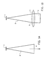
- FIGURE 1A shows an arbitrary source 1 that emits a diverging charged particle beam 2.
- a collimated beam 3 i.e. a beam, which is substantially parallel
- a collimator lens 4 as shown (schematically) in FIGURE 1B or collimation assembly is positioned in the beam trajectory to collimate the diverging charged particle beam 2.
- the collimation takes place in the collimation plane or principal plane 5 of the collimator 4, denoted in FIGURE 1B by the dotted line.
- the (almost) parallel charged particle beam can be split in a plurality of beamlets, which are subsequently focused on a target for pattern exposure, inspection, observation or other purposes.
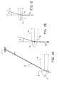
- FIGURE 2 shows the trajectory of a small portion of the diverging charged particle beam 2, which is refracted in the collimator plane at collimation point 6.
- the angle between the initial direction and the final direction is denoted by ⁇ . In an ideal situation all emitted charged particles seem to originate from a singularity on the emission surface of the source 1.
- the charged particle path of a charged particle emitted from said source 1 is not as well defined as shown in FIGURE 2 .
- the source size seen from said collimation point 6 looking upward to the source, is not a singularity. It has a finite size as shown in FIGURE 3A .
- the finite size induces a finite angle ⁇ , called the intrinsic opening angle of the charged particle beam.
- the diffraction angle of each charged particle in the collimation plane 5 is not as well-defined as shown in FIGURE 2 .
- FIGURE 3B shows a detail around point 6 of figure 3A .
- the aberrations will become a problem when the beam is for instance projected on a target for exposure in lithography systems or for observation in microscopy systems in which applications a very small spot size is desired. Due to the aberrations the beamlet will get blurred and the spot size of the beamlet is no longer well-defined, which results in a blurry pattern or image. This is especially the case when angle ⁇ comes in the order of the intrinsic opening angle ⁇ of the charged particle beam.
- the source size or source image size scale with ( ⁇ + ⁇ ) * l , wherein l is the distance between the collimation plane 5 and the source 1.
- the influence of aberration ⁇ on the focused spot size of the emitted charged particle beam scales with ⁇ * l . Now if ⁇ is of the same order as or larger than the intrinsic opening angle ⁇ , a significant reduction of resolution results.
- the apparatus of the present invention provides a solution to overcome the negative influences of the chromatic aberrations.
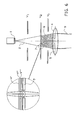
- the influence of these aberrations is avoided by positioning a lens array 7 having a plurality of lenses between said source 1 and said collimator lens 4 as is depicted in FIGURE 4 .
- said lens array 7 is positioned in such a way that each lens of the lens array projects an image of said source on said collimation plane 5.
- the internal opening angle in the beam is determined by the size of the beamlet in the lens array, d, and the distance between said lens array and the collimation plane, f, as d/f.
- the intrinsic angle ⁇ can be made substantially larger than the aberration ⁇ , and the blur in the system will therefore not increase.
- the invention can be further improved by adding additional splitting means into the system, preferably located between the source 1 and the lens array 7.
- the splitting means split the diverging charged particle beam 2 in a plurality of diverging charged particle beamlets 11.
- the splitting means comprise a spatial filter, preferably an aperture array 10 as is depicted in FIGURE 5 . Adding an aperture array 10 at this position into the system provides a way to reduce the heat load on the lens array 7. It furthermore enhances the performance of the lens array 7 located behind (when following the optical pathway of the charged particle beamlets) said splitting means.
- the invention can be improved further by adding opening angle limiting means, preferably an aperture array, in the optical pathway of said plurality of charged particle beamlets behind said collimator lens 4 or collimator lens assembly.
- the opening angle limiting means are arranged to limit the opening angle of the beamlets that have passed the collimation plane and corrects for additional third order aberrations induced by said collimation lens 4.
- any array of conventional charged particle lenses can be used. It is also possible, however, to use the embodiment shown in FIGURE 6 .
- FIGURE 6 three plates are installed, each at its own potential V1, V2 and V3. In fact, only the plane at V1 or at V3, together with the apperture plate 7 at V2, are actually needed in order to have a lens effect.
- the plates at V1 and V3 have a hole large enough to let the beam 2 pass without interfering with the beam 2.
- Plate 7 is in fact the actual lens array. Plate 7 here is a plate with holes at the location where beamlets 8 should be created. In FIGURE 6 an enlarged detail of one of the holes in plate 7 is shown. In this enlarged view, the equipotential surfaces (indicated V', V", V'”) are added, as well as the trajectory of two charged particles. Due to the shape of the equipotential surfaces, there will be a focussing effect on the charged particle beamlets resulting from plate 7.
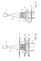
- FIGURE 7 instead of a conventional charged particle collimating lens 4, a deflector array is used for collimating.
- This deflector has holes at the location of the beamlets 8, and electrodes at voltages V1---V6 (for the three deflectors shown).
- V1---V6 for the three deflectors shown.
- FIGURE 8 A layout for such a system is shown in FIGURE 8 .
- lens array 7 is put on a Voltage V1.
- V1 Voltage
- V2 voltage
- V3 voltage
- FIGURES 4 and 7 can be combined in a way shown in FIGURE 9 , in which way it leads to additional advantages.
- the collimator lens 4 has a collimating effect with some spherical aberration, depicted as an over collimation of the outside bealets in figure 9 .
- a deflector array is now located. This deflector array has its deflectors aligned with the beamlets 9. When the voltages of the deflectors are properly set, is possible to correct the spherical aberration of the collimator lens 4 using only relatively low voltages.
- the voltage of each deflector should be set in such a way that its deflecting effect on the charged particle beamlet passing the deflector is proportional to the distance of the deflector from the optical axis of the collimator lens 4 to the third power.
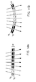
- the lens array 7 used in the present invention is preferably an electrostatic lens array 12.
- FIGURE 10A schematically shows an example of such a lens array 12.
- the lens array 12 comprises two conducting plates with holes, positioned in close proximity to each other wherein said holes in each plate are substantially aligned with each other. An electric field is applied between the two plates by applying a voltage difference V 1 - V 2 between said plates as shown in FIGURE 10A .
- Focusing a diverging charged particle beam may induce a further problem.
- Each beam passing through a planar electrostatic lens array 12 is not focused correctly due to the fact that the incoming beamlets are not passing the lenses perpendicular to the lens plane (i.e., parallel to the lens axis). This complication affects the performance of the system, i.e. additional aberrations are introduced.
- each beamlet passes the lens array 13 through the holes substantially perpendicular to the surface of both plates.
- the charged particle beam that is used can be any charged particle beam known in the art, but preferably an electron beam or ion beam.
- the invention can be used in a lithography system or microscopy system. In a lithography system the invention provides a way to pattern a substrate to be patterned with enhanced resolution, since the spot size of the charged particle beam is kept small. Furthermore in microscopy systems objects can be imaged with higher resolution.
Landscapes
- Chemical & Material Sciences (AREA)
- Engineering & Computer Science (AREA)
- Analytical Chemistry (AREA)
- Nanotechnology (AREA)
- Crystallography & Structural Chemistry (AREA)
- Physics & Mathematics (AREA)
- Theoretical Computer Science (AREA)
- Mathematical Physics (AREA)
- Condensed Matter Physics & Semiconductors (AREA)
- General Physics & Mathematics (AREA)
- Manufacturing & Machinery (AREA)
- Electron Beam Exposure (AREA)
- Electron Sources, Ion Sources (AREA)
Applications Claiming Priority (2)
| Application Number | Priority Date | Filing Date | Title |
|---|---|---|---|
| US45374503P | 2003-03-10 | 2003-03-10 | |
| EP04719157A EP1602121B1 (fr) | 2003-03-10 | 2004-03-10 | Dispositif servant a generer une pluralite de petits faisceaux |
Related Parent Applications (1)
| Application Number | Title | Priority Date | Filing Date |
|---|---|---|---|
| EP04719157A Division EP1602121B1 (fr) | 2003-03-10 | 2004-03-10 | Dispositif servant a generer une pluralite de petits faisceaux |
Publications (2)
| Publication Number | Publication Date |
|---|---|
| EP2503587A2 true EP2503587A2 (fr) | 2012-09-26 |
| EP2503587A3 EP2503587A3 (fr) | 2017-08-23 |
Family
ID=32990809
Family Applications (2)
| Application Number | Title | Priority Date | Filing Date |
|---|---|---|---|
| EP04719157A Expired - Lifetime EP1602121B1 (fr) | 2003-03-10 | 2004-03-10 | Dispositif servant a generer une pluralite de petits faisceaux |
| EP12172592.3A Withdrawn EP2503587A3 (fr) | 2003-03-10 | 2004-03-10 | Appareil de génération de plusieurs mini-faisceaux |
Family Applications Before (1)
| Application Number | Title | Priority Date | Filing Date |
|---|---|---|---|
| EP04719157A Expired - Lifetime EP1602121B1 (fr) | 2003-03-10 | 2004-03-10 | Dispositif servant a generer une pluralite de petits faisceaux |
Country Status (6)
| Country | Link |
|---|---|
| US (5) | US7129502B2 (fr) |
| EP (2) | EP1602121B1 (fr) |
| JP (1) | JP4484868B2 (fr) |
| KR (1) | KR101068607B1 (fr) |
| CN (1) | CN1759465B (fr) |
| WO (1) | WO2004081910A2 (fr) |
Cited By (2)
| Publication number | Priority date | Publication date | Assignee | Title |
|---|---|---|---|---|
| EP3576128A1 (fr) * | 2018-05-28 | 2019-12-04 | ASML Netherlands B.V. | Appareil à faisceau d'électrons, outil d'inspection et procédé d'inspection |
| EP4734147A1 (fr) * | 2024-10-24 | 2026-04-29 | ASML Netherlands B.V. | Dispositif optique à particules chargées pour un appareil à faisceau de particules chargées |
Families Citing this family (214)
| Publication number | Priority date | Publication date | Assignee | Title |
|---|---|---|---|---|
| KR101068607B1 (ko) * | 2003-03-10 | 2011-09-30 | 마퍼 리쏘그라피 아이피 비.브이. | 복수 개의 빔렛 발생 장치 |
| CN102709143B (zh) * | 2003-09-05 | 2016-03-09 | 卡尔蔡司Smt有限责任公司 | 电子光学排布结构、多电子分束检验系统和方法 |
| KR101099487B1 (ko) * | 2004-05-17 | 2011-12-28 | 마퍼 리쏘그라피 아이피 비.브이. | 대전 입자 빔 노광 시스템 |
| JP2008527750A (ja) * | 2005-01-14 | 2008-07-24 | アラディアンス インコーポレイテッド | 同期ラスタ走査リソグラフィ・システム |
| US8304749B2 (en) * | 2005-02-11 | 2012-11-06 | Ims Nanofabrication Ag | Charged-particle exposure apparatus with electrostatic zone plate |
| NL1029132C2 (nl) * | 2005-05-26 | 2006-11-28 | Univ Delft Tech | Inrichting voor het opwekken van evenwijdige stralenbundeldelen. |
| CN101248505B (zh) * | 2005-07-08 | 2010-12-15 | 耐克斯金思美控股公司 | 受控粒子束制造用的设备和方法 |
| JP5663717B2 (ja) | 2005-09-06 | 2015-02-04 | カール ツァイス マイクロスコピー ゲーエムベーハーCarl Zeiss Microscopy Gmbh | 荷電粒子システム |
| US7557338B2 (en) * | 2006-03-14 | 2009-07-07 | Avago Technologies General Ip (Singapore) Pte. Ltd. | Electronic device with integrated optical navigation module and microlens array therefore |
| US8134135B2 (en) | 2006-07-25 | 2012-03-13 | Mapper Lithography Ip B.V. | Multiple beam charged particle optical system |
| KR101464388B1 (ko) * | 2006-07-25 | 2014-11-21 | 마퍼 리쏘그라피 아이피 비.브이. | 다중 빔 대전 입자 광학 시스템 |
| KR101423408B1 (ko) * | 2006-07-25 | 2014-07-24 | 마퍼 리쏘그라피 아이피 비.브이. | 대전 입자 리소그래피 시스템 |
| WO2008140585A1 (fr) | 2006-11-22 | 2008-11-20 | Nexgen Semi Holding, Inc. | Appareil et procédé de fabrication de masque conforme |
| JP2010519697A (ja) * | 2007-02-22 | 2010-06-03 | アプライド マテリアルズ イスラエル リミテッド | 高スループットsemツール |
| EP2019415B1 (fr) | 2007-07-24 | 2016-05-11 | IMS Nanofabrication AG | Source multifaisceaux |
| US8445869B2 (en) | 2008-04-15 | 2013-05-21 | Mapper Lithography Ip B.V. | Projection lens arrangement |
| US8890094B2 (en) | 2008-02-26 | 2014-11-18 | Mapper Lithography Ip B.V. | Projection lens arrangement |
| WO2009127659A2 (fr) | 2008-04-15 | 2009-10-22 | Mapper Lithography Ip B.V. | Eliminateur de faisceaux |
| US7851774B2 (en) * | 2008-04-25 | 2010-12-14 | Taiwan Semiconductor Manufacturing Company, Ltd. | System and method for direct writing to a wafer |
| US10991545B2 (en) | 2008-06-30 | 2021-04-27 | Nexgen Semi Holding, Inc. | Method and device for spatial charged particle bunching |
| US10566169B1 (en) | 2008-06-30 | 2020-02-18 | Nexgen Semi Holding, Inc. | Method and device for spatial charged particle bunching |
| KR20110139699A (ko) | 2009-02-22 | 2011-12-29 | 마퍼 리쏘그라피 아이피 비.브이. | 리소그래피 장치 및 기판 핸들링 배열체 |
| KR101687955B1 (ko) | 2009-02-22 | 2016-12-20 | 마퍼 리쏘그라피 아이피 비.브이. | 하전입자 리소그래피 장치 및 진공 챔버에 진공을 발생시키는 방법 |
| EP2399272A1 (fr) | 2009-02-22 | 2011-12-28 | Mapper Lithography IP B.V. | Procédé et agencement pour obtenir un vide dans une chambre à vide |
| CN102422380A (zh) | 2009-02-22 | 2012-04-18 | 迈普尔平版印刷Ip有限公司 | 带电粒子微影设备及真空腔室中产生真空的方法 |
| KR101614460B1 (ko) | 2009-05-20 | 2016-04-21 | 마퍼 리쏘그라피 아이피 비.브이. | 리소그래피 시스템을 위한 패턴 데이터 전환 |
| CN102460632B (zh) | 2009-05-20 | 2015-11-25 | 迈普尔平版印刷Ip有限公司 | 产生二级图案以供光刻处理的方法和使用该方法的图案产生器 |
| CN102460631B (zh) | 2009-05-20 | 2015-03-25 | 迈普尔平版印刷Ip有限公司 | 两次扫描 |
| EP2494579B1 (fr) | 2009-10-26 | 2017-08-02 | Mapper Lithography IP B.V. | Système de lithographie à multiples petits faisceaux de particules chargées, dispositif de modulation et procédé de fabrication de celui-ci |
| US8952342B2 (en) * | 2009-12-17 | 2015-02-10 | Mapper Lithography Ip B.V. | Support and positioning structure, semiconductor equipment system and method for positioning |
| WO2011130092A1 (fr) * | 2010-04-14 | 2011-10-20 | The Regents Of The University Of California | Procédé et appareil pour pulvérisation cathodique avec une lentille plasma |
| CN103069533B (zh) * | 2010-08-26 | 2017-11-17 | 利乐拉瓦尔集团及财务有限公司 | 用于电子束产生装置的控制网格设计 |
| KR101725299B1 (ko) | 2010-10-26 | 2017-04-10 | 마퍼 리쏘그라피 아이피 비.브이. | 변조 디바이스 및 이를 사용하는 하전 입자 멀티-빔렛 리소그래피 시스템 |
| US9305747B2 (en) | 2010-11-13 | 2016-04-05 | Mapper Lithography Ip B.V. | Data path for lithography apparatus |
| US8884255B2 (en) | 2010-11-13 | 2014-11-11 | Mapper Lithography Ip B.V. | Data path for lithography apparatus |
| US8604411B2 (en) | 2010-11-13 | 2013-12-10 | Mapper Lithography Ip B.V. | Charged particle beam modulator |
| EP2638560B1 (fr) | 2010-11-13 | 2017-02-22 | Mapper Lithography IP B.V. | Système de lithographie par particules chargées à refroidissement par réseau d'ouvertures |
| WO2012062932A1 (fr) | 2010-11-13 | 2012-05-18 | Mapper Lithography Ip B.V. | Système de lithographie à particules chargées doté d'une chambre intermédiaire |
| WO2012062854A1 (fr) * | 2010-11-13 | 2012-05-18 | Mapper Lithography Ip B.V. | Système de lithographie et procédé de réfraction |
| JP6158091B2 (ja) | 2010-12-14 | 2017-07-05 | マッパー・リソグラフィー・アイピー・ビー.ブイ. | リソグラフィシステム及びこのようなリソグラフィシステムで基板を処理する方法 |
| CN103477285A (zh) | 2011-02-16 | 2013-12-25 | 迈普尔平版印刷Ip有限公司 | 用于磁屏蔽的系统 |
| JP5951753B2 (ja) | 2011-04-22 | 2016-07-13 | マッパー・リソグラフィー・アイピー・ビー.ブイ. | リソグラフィ機のクラスタのためのネットワークアーキテクチャおよびプロトコル |
| US8936994B2 (en) * | 2011-04-28 | 2015-01-20 | Mapper Lithography Ip B.V. | Method of processing a substrate in a lithography system |
| TW201330705A (zh) | 2011-09-28 | 2013-07-16 | Mapper Lithography Ip Bv | 電漿產生器 |
| WO2013132064A2 (fr) | 2012-03-08 | 2013-09-12 | Mapper Lithography Ip B.V. | Système de lithographie à particules chargées pourvu d'un capteur d'alignement et d'un capteur de mesure de faisceau |
| US9123507B2 (en) | 2012-03-20 | 2015-09-01 | Mapper Lithography Ip B.V. | Arrangement and method for transporting radicals |
| US11348756B2 (en) | 2012-05-14 | 2022-05-31 | Asml Netherlands B.V. | Aberration correction in charged particle system |
| EP2850635B1 (fr) | 2012-05-14 | 2016-04-27 | Mapper Lithography IP B.V. | Procédé de fabrication de système lithographique à petits faisceaux multiples de particules chargées et de système de refroidissement |
| US10586625B2 (en) | 2012-05-14 | 2020-03-10 | Asml Netherlands B.V. | Vacuum chamber arrangement for charged particle beam generator |
| NL2010759C2 (en) | 2012-05-14 | 2015-08-25 | Mapper Lithography Ip Bv | Modulation device and power supply arrangement. |
| CN107359101B (zh) | 2012-05-14 | 2019-07-12 | Asml荷兰有限公司 | 带电粒子射束产生器中的高电压屏蔽和冷却 |
| US20140034484A1 (en) * | 2012-07-31 | 2014-02-06 | Andrew E. Fisk | Device for the elimination of liquid droplets from a cathodic arc plasma source |
| NL2010760C2 (en) | 2013-05-03 | 2014-11-04 | Mapper Lithography Ip Bv | Beam grid layout. |
| US9922801B2 (en) | 2013-08-23 | 2018-03-20 | Mapper Lithography Ip B.V. | Drying apparatus for use in a lithography system |
| US9903688B2 (en) * | 2013-11-08 | 2018-02-27 | Supas Ltd | Scope |
| NL2013814B1 (en) | 2013-11-14 | 2016-05-10 | Mapper Lithography Ip Bv | Multi-electrode vacuum arrangement. |
| JP6590811B2 (ja) | 2013-12-30 | 2019-10-16 | エーエスエムエル ネザーランズ ビー.ブイ. | 陰極構成体、電子銃、及びこのような電子銃を有するリソグラフィシステム |
| US9390891B2 (en) | 2014-08-15 | 2016-07-12 | Taiwan Semiconductor Manufacturing Company, Ltd. | Apparatus for charged particle lithography system |
| KR20170084240A (ko) | 2014-11-14 | 2017-07-19 | 마퍼 리쏘그라피 아이피 비.브이. | 리소그래피 시스템에서 기판을 이송하기 위한 로드 로크 시스템 및 방법 |
| DE102015202172B4 (de) | 2015-02-06 | 2017-01-19 | Carl Zeiss Microscopy Gmbh | Teilchenstrahlsystem und Verfahren zur teilchenoptischen Untersuchung eines Objekts |
| US9484188B2 (en) | 2015-03-11 | 2016-11-01 | Mapper Lithography Ip B.V. | Individual beam pattern placement verification in multiple beam lithography |
| US9922799B2 (en) | 2015-07-21 | 2018-03-20 | Hermes Microvision, Inc. | Apparatus of plural charged-particle beams |
| KR20240042242A (ko) * | 2015-07-22 | 2024-04-01 | 에이에스엠엘 네델란즈 비.브이. | 복수의 하전 입자 빔을 이용하는 장치 |
| US10096450B2 (en) | 2015-12-28 | 2018-10-09 | Mapper Lithography Ip B.V. | Control system and method for lithography apparatus |
| CN108885187B (zh) | 2016-01-27 | 2021-05-25 | Asml 荷兰有限公司 | 多个带电粒子束的装置 |
| US9981293B2 (en) | 2016-04-21 | 2018-05-29 | Mapper Lithography Ip B.V. | Method and system for the removal and/or avoidance of contamination in charged particle beam systems |
| DE202017102973U1 (de) | 2016-05-17 | 2017-10-18 | A-Gruppen | Werkzeugträger mit Kettenantrieb und niedrigem Schwerpunkt |
| US9922796B1 (en) * | 2016-12-01 | 2018-03-20 | Applied Materials Israel Ltd. | Method for inspecting a specimen and charged particle multi-beam device |
| US10347460B2 (en) | 2017-03-01 | 2019-07-09 | Dongfang Jingyuan Electron Limited | Patterned substrate imaging using multiple electron beams |
| DE102018202421B3 (de) | 2018-02-16 | 2019-07-11 | Carl Zeiss Microscopy Gmbh | Vielstrahl-Teilchenstrahlsystem |
| DE102018202428B3 (de) | 2018-02-16 | 2019-05-09 | Carl Zeiss Microscopy Gmbh | Vielstrahl-Teilchenmikroskop |
| CN112055886A (zh) | 2018-02-27 | 2020-12-08 | 卡尔蔡司MultiSEM有限责任公司 | 带电粒子多束系统及方法 |
| WO2019211072A1 (fr) * | 2018-05-01 | 2019-11-07 | Asml Netherlands B.V. | Appareil d'injection à faisceaux multiples |
| US10811215B2 (en) | 2018-05-21 | 2020-10-20 | Carl Zeiss Multisem Gmbh | Charged particle beam system |
| DE102018115012A1 (de) | 2018-06-21 | 2019-12-24 | Carl Zeiss Microscopy Gmbh | Teilchenstrahlsystem |
| DE102018007455B4 (de) | 2018-09-21 | 2020-07-09 | Carl Zeiss Multisem Gmbh | Verfahren zum Detektorabgleich bei der Abbildung von Objekten mittels eines Mehrstrahl-Teilchenmikroskops, System sowie Computerprogrammprodukt |
| DE102018007652B4 (de) | 2018-09-27 | 2021-03-25 | Carl Zeiss Multisem Gmbh | Teilchenstrahl-System sowie Verfahren zur Stromregulierung von Einzel-Teilchenstrahlen |
| DE102018124044B3 (de) | 2018-09-28 | 2020-02-06 | Carl Zeiss Microscopy Gmbh | Verfahren zum Betreiben eines Vielstrahl-Teilchenstrahlmikroskops und Vielstrahl-Teilchenstrahlsystem |
| DE102018124219A1 (de) | 2018-10-01 | 2020-04-02 | Carl Zeiss Microscopy Gmbh | Vielstrahl-Teilchenstrahlsystem und Verfahren zum Betreiben eines solchen |
| US11373838B2 (en) * | 2018-10-17 | 2022-06-28 | Kla Corporation | Multi-beam electron characterization tool with telecentric illumination |
| NL2022156B1 (en) | 2018-12-10 | 2020-07-02 | Asml Netherlands Bv | Plasma source control circuit |
| WO2020141031A1 (fr) | 2018-12-31 | 2020-07-09 | Asml Netherlands B.V. | Appareil d'inspection à faisceaux multiples |
| TWI743626B (zh) | 2019-01-24 | 2021-10-21 | 德商卡爾蔡司多重掃描電子顯微鏡有限公司 | 包含多束粒子顯微鏡的系統、對3d樣本逐層成像之方法及電腦程式產品 |
| CN111477530B (zh) | 2019-01-24 | 2023-05-05 | 卡尔蔡司MultiSEM有限责任公司 | 利用多束粒子显微镜对3d样本成像的方法 |
| KR20240095476A (ko) * | 2019-05-31 | 2024-06-25 | 에이에스엠엘 네델란즈 비.브이. | 다중 하전 입자 빔 장치 및 그 작동 방법 |
| DE102019004124B4 (de) | 2019-06-13 | 2024-03-21 | Carl Zeiss Multisem Gmbh | Teilchenstrahl-System zur azimutalen Ablenkung von Einzel-Teilchenstrahlen sowie seine Verwendung und Verfahren zur Azimut-Korrektur bei einem Teilchenstrahl-System |
| DE102019005362A1 (de) | 2019-07-31 | 2021-02-04 | Carl Zeiss Multisem Gmbh | Verfahren zum Betreiben eines Vielzahl-Teilchenstrahlsystems unter Veränderung der numerischen Apertur, zugehöriges Computerprogrammprodukt und Vielzahl-Teilchenstrahlsystem |
| WO2021071357A1 (fr) | 2019-10-08 | 2021-04-15 | Technische Universiteit Delft | Dispositif pour générer une pluralité de petits faisceaux de particules chargées, et appareil d'inspection, d'imagerie ou de traitement et son procédé d'utilisation |
| NL2024065B1 (en) * | 2019-10-21 | 2021-06-22 | Univ Delft Tech | Multi-beam charged particle source with alignment means |
| DE102019008249B3 (de) | 2019-11-27 | 2020-11-19 | Carl Zeiss Multisem Gmbh | Teilchenstrahl-System mit einer Multistrahl-Ablenkeinrichtung und einem Strahlfänger, Verfahren zum Betreiben des Teilchenstrahl-Systems und zugehöriges Computerprogrammprodukt |
| WO2021104991A1 (fr) | 2019-11-28 | 2021-06-03 | Asml Netherlands B.V. | Appareil d'éclairage à particules chargées à sources multiples |
| TWI773020B (zh) * | 2019-12-19 | 2022-08-01 | 荷蘭商Asml荷蘭公司 | 用於色像差減輕之系統及方法 |
| EP3937204A1 (fr) | 2020-07-06 | 2022-01-12 | ASML Netherlands B.V. | Appareil d'inspection |
| EP3975222A1 (fr) | 2020-09-24 | 2022-03-30 | ASML Netherlands B.V. | Outil d'évaluation de particules chargées, procédé d'inspection |
| KR102830218B1 (ko) | 2020-01-06 | 2025-07-08 | 에이에스엠엘 네델란즈 비.브이. | 하전 입자 평가 툴, 검사 방법 |
| EP4100986A1 (fr) | 2020-02-04 | 2022-12-14 | Carl Zeiss MultiSEM GmbH | Balayage numérique à faisceaux multiples et acquisition d'image |
| EP3869535A1 (fr) | 2020-02-21 | 2021-08-25 | ASML Netherlands B.V. | Outil d'évaluation de particules chargées, procédé d'inspection |
| EP3869533A1 (fr) * | 2020-02-21 | 2021-08-25 | ASML Netherlands B.V. | Outil d'évaluation à particules chargées, procédé d'inspection |
| IL295627A (en) | 2020-02-21 | 2022-10-01 | Asml Netherlands Bv | Inspection apparatus |
| KR102817129B1 (ko) | 2020-02-21 | 2025-06-05 | 에이에스엠엘 네델란즈 비.브이. | 하전 입자 검사 툴, 검사 방법 |
| EP3869536A1 (fr) | 2020-02-21 | 2021-08-25 | ASML Netherlands B.V. | Appareil d'inspection |
| JP7689139B2 (ja) | 2020-03-12 | 2025-06-05 | カール ツァイス マルティセム ゲゼルシヤフト ミット ベシュレンクテル ハフツング | マルチビーム発生ユニットおよびマルチビーム偏向ユニットの特定の改善 |
| DE102020107738B3 (de) | 2020-03-20 | 2021-01-14 | Carl Zeiss Multisem Gmbh | Teilchenstrahl-System mit einer Multipol-Linsen-Sequenz zur unabhängigen Fokussierung einer Vielzahl von Einzel-Teilchenstrahlen, seine Verwendung und zugehöriges Verfahren |
| EP3893264A1 (fr) | 2020-04-06 | 2021-10-13 | ASML Netherlands B.V. | Outil d'évaluation par particules chargées, procédé d'inspection |
| EP4020565A1 (fr) | 2020-12-23 | 2022-06-29 | ASML Netherlands B.V. | Substrat de détecteur, appareil d'inspection et procédé d'évaluation d'échantillons |
| KR102827024B1 (ko) | 2020-07-06 | 2025-07-02 | 에이에스엠엘 네델란즈 비.브이. | 하전 입자 다중-빔 평가 도구에 사용하기 위한 검출기 기판 |
| KR20230065267A (ko) | 2020-09-07 | 2023-05-11 | 에이에스엠엘 네델란즈 비.브이. | 전자기 차폐부를 포함하는 전자-광학 조립체 |
| DE102020123567B4 (de) | 2020-09-09 | 2025-02-13 | Carl Zeiss Multisem Gmbh | Vielzahl-Teilchenstrahl-System mit Kontrast-Korrektur-Linsen-System |
| EP3971940A1 (fr) | 2020-09-17 | 2022-03-23 | ASML Netherlands B.V. | Ensemble réseau de lentille d'objectif, système d'optique électronique, réseau de système d'optique électronique, procédé de mise au point, agencement de lentille d'objectif |
| IL300807A (en) | 2020-09-17 | 2023-04-01 | Asml Netherlands Bv | Charged particle evaluation tool test method |
| EP4214737A1 (fr) | 2020-09-17 | 2023-07-26 | ASML Netherlands B.V. | Ensemble de réseau de lentilles d'objectif, système électro-optique, réseau de systèmes électro-optiques, procédé de focalisation, agencement de lentille d'objectif |
| EP3971939A1 (fr) | 2020-09-17 | 2022-03-23 | ASML Netherlands B.V. | Outil d'évaluation de particules chargées, procédé d'inspection |
| TW202220012A (zh) | 2020-09-30 | 2022-05-16 | 德商卡爾蔡司多重掃描電子顯微鏡有限公司 | 在可調工作距離附近具快速自動對焦之多重粒子束顯微鏡及相關方法 |
| EP4002421A1 (fr) | 2020-11-12 | 2022-05-25 | ASML Netherlands B.V. | Ensemble réseau de lentille d'objectif, système d'optique électronique, réseau de système d'optique électronique, procédé de mise au point |
| IL302654A (en) | 2020-11-12 | 2023-07-01 | Asml Netherlands Bv | Assembling an objective lens array, electronic-optical system, electronic-optical system array, focusing method |
| EP4009348A1 (fr) | 2020-12-01 | 2022-06-08 | ASML Netherlands B.V. | Dispositif et procédé d'inspection à particules chargées |
| EP4009349A1 (fr) | 2020-12-03 | 2022-06-08 | ASML Netherlands B.V. | Outil de particules chargées, procédé d'étalonnage, procédé d'inspection |
| EP4086933A1 (fr) | 2021-05-03 | 2022-11-09 | ASML Netherlands B.V. | Système de particules chargées, procédé de traitement d'un échantillon à l'aide d'un faisceau multiple de particules chargées |
| IL303577A (en) | 2020-12-14 | 2023-08-01 | Asml Netherlands Bv | Charged particle system, a sample processing method using multiple beams of charged particles |
| JP2024501654A (ja) | 2020-12-23 | 2024-01-15 | エーエスエムエル ネザーランズ ビー.ブイ. | 荷電粒子光学デバイス |
| EP4020516A1 (fr) | 2020-12-23 | 2022-06-29 | ASML Netherlands B.V. | Dispositif optique à particules chargées, ensemble lentilles d'objectif, détecteur, réseau de détecteurs et procédés |
| DE102021200799B3 (de) | 2021-01-29 | 2022-03-31 | Carl Zeiss Multisem Gmbh | Verfahren mit verbesserter Fokuseinstellung unter Berücksichtigung eines Bildebenenkipps in einem Vielzahl-Teilchenstrahlmikroskop |
| EP4084039A1 (fr) | 2021-04-29 | 2022-11-02 | ASML Netherlands B.V. | Système et procédé d'évaluation de particules chargées |
| IL308010A (en) | 2021-05-12 | 2023-12-01 | Asml Netherlands Bv | Evaluation system, evaluation method |
| EP4089712A1 (fr) | 2021-05-12 | 2022-11-16 | ASML Netherlands B.V. | Système d'évaluation, procédé d'évaluation |
| EP4092712A1 (fr) | 2021-05-18 | 2022-11-23 | ASML Netherlands B.V. | Dispositif optique à particules chargées et méthode utilisant un tel dispositif |
| EP4092614A1 (fr) | 2021-05-21 | 2022-11-23 | ASML Netherlands B.V. | Dispositif et procédé de traitement de données, système et procédé d'évaluation de particules chargées |
| EP4341890A1 (fr) | 2021-05-21 | 2024-03-27 | ASML Netherlands B.V. | Dispositif et procédé de traitement de données, système et procédé d'évaluation de particules chargées |
| EP4095881A1 (fr) | 2021-05-25 | 2022-11-30 | ASML Netherlands B.V. | Dispositif de particules chargées |
| TW202312205A (zh) | 2021-05-27 | 2023-03-16 | 德商卡爾蔡司多重掃描電子顯微鏡有限公司 | 多重射束帶電粒子系統與在多重射束帶電粒子系統中控制工作距離的方法 |
| EP4102536A1 (fr) | 2021-06-10 | 2022-12-14 | ASML Netherlands B.V. | Procédé de compensation d'un effet de distorsion d'électrode, système d'évaluation |
| EP4113570A1 (fr) | 2021-06-29 | 2023-01-04 | ASML Netherlands B.V. | Système d'évaluation de particules chargées et procédé d'alignement d'un échantillon dans un système d'évaluation de particules chargées |
| DE102021116969B3 (de) | 2021-07-01 | 2022-09-22 | Carl Zeiss Multisem Gmbh | Verfahren zur bereichsweisen Probeninspektion mittels eines Vielstrahl-Teilchenmikroskopes, Computerprogrammprodukt und Vielstrahl-Teilchenmikroskop zur Halbleiterprobeninspektion |
| EP4117015A1 (fr) | 2021-07-05 | 2023-01-11 | ASML Netherlands B.V. | Dispositif, détecteur et procédés de particules chargées |
| EP4117016A1 (fr) | 2021-07-05 | 2023-01-11 | ASML Netherlands B.V. | Détecteur de particules chargées |
| EP4117017A1 (fr) | 2021-07-05 | 2023-01-11 | ASML Netherlands B.V. | Détecteur de particules chargées |
| WO2023280551A1 (fr) | 2021-07-07 | 2023-01-12 | Asml Netherlands B.V. | Appareil et procédé à particules chargées |
| EP4117014A1 (fr) | 2021-07-07 | 2023-01-11 | ASML Netherlands B.V. | Appareil et procédé de particules chargées |
| EP4117012A1 (fr) | 2021-07-07 | 2023-01-11 | ASML Netherlands B.V. | Dispositif optique à particules chargées, appareil et procédé à particules chargées |
| EP4123683A1 (fr) | 2021-07-20 | 2023-01-25 | ASML Netherlands B.V. | Dispositif et procédé de traitement de données, système et procédé d'évaluation de particules chargées |
| EP4131329A1 (fr) | 2021-08-02 | 2023-02-08 | ASML Netherlands B.V. | Dispositif optique à particules chargées |
| EP4156227A1 (fr) | 2021-09-27 | 2023-03-29 | ASML Netherlands B.V. | Appareil et procédé de particules chargées |
| US11651934B2 (en) | 2021-09-30 | 2023-05-16 | Kla Corporation | Systems and methods of creating multiple electron beams |
| KR20240093780A (ko) | 2021-10-19 | 2024-06-24 | 에이에스엠엘 네델란즈 비.브이. | 검출기 조립체, 하전 입자 디바이스, 장치, 및 방법 |
| EP4170695A1 (fr) | 2021-10-19 | 2023-04-26 | ASML Netherlands B.V. | Ensemble détecteur, dispositif de particules chargées, appareil et procédés |
| EP4181167A1 (fr) | 2021-11-11 | 2023-05-17 | ASML Netherlands B.V. | Système et procédé d'évaluation avec des particules chargées |
| KR20240095241A (ko) | 2021-11-11 | 2024-06-25 | 에이에스엠엘 네델란즈 비.브이. | 하전 입자 평가 시스템 및 방법 |
| KR20240122824A (ko) | 2021-12-15 | 2024-08-13 | 에이에스엠엘 네델란즈 비.브이. | 샘플 맵을 생성하는 방법, 컴퓨터 프로그램 제품 |
| EP4213176A1 (fr) | 2022-01-13 | 2023-07-19 | ASML Netherlands B.V. | Système d'évaluation à particules chargées |
| WO2023110244A1 (fr) | 2021-12-15 | 2023-06-22 | Asml Netherlands B.V. | Système d'évaluation de particules chargées |
| WO2023110331A1 (fr) | 2021-12-17 | 2023-06-22 | Asml Netherlands B.V. | Appareil optique à particules chargées et procédé de projection |
| EP4199027A1 (fr) | 2021-12-17 | 2023-06-21 | ASML Netherlands B.V. | Appareil à particules chargées, appareil à dispositifs multiples, procédé d'utilisation de l'appareil à particules chargées et procédé de commande |
| EP4199032A1 (fr) | 2021-12-17 | 2023-06-21 | ASML Netherlands B.V. | Dispositif d'inspection de détecteur, ensemble détecteur, réseau de détecteurs, appareil et procédé |
| KR20240115321A (ko) | 2021-12-17 | 2024-07-25 | 에이에스엠엘 네델란즈 비.브이. | 검출기 검사 디바이스, 검출기 조립체, 검출기 어레이, 장치, 및 방법 |
| EP4199031A1 (fr) | 2021-12-17 | 2023-06-21 | ASML Netherlands B.V. | Appareil optique à particules chargées et procédé de projection |
| EP4199033A1 (fr) | 2021-12-20 | 2023-06-21 | ASML Netherlands B.V. | Procédé de traitement d'un échantillon avec un système d'évaluation de particules chargées |
| EP4199028A1 (fr) | 2021-12-20 | 2023-06-21 | ASML Netherlands B.V. | Dispositif à particules chargées, appareil d'évaluation de particules chargées, procédé de mesure, et procédé de surveillance |
| WO2023117277A1 (fr) * | 2021-12-23 | 2023-06-29 | Asml Netherlands B.V. | Dispositif électro-optique, procédé de compensation des variations d'une propriété de sous-faisceaux |
| EP4202969A1 (fr) * | 2021-12-23 | 2023-06-28 | ASML Netherlands B.V. | Dispositif électro-optique avec compensation de variations d'une caractéristique de sous-faisceaux |
| EP4202970A1 (fr) | 2021-12-24 | 2023-06-28 | ASML Netherlands B.V. | Procédé de détermination d'alignement et programme informatique |
| EP4250331A1 (fr) | 2022-03-22 | 2023-09-27 | ASML Netherlands B.V. | Appareil et procédé de particules chargées |
| EP4258320A1 (fr) | 2022-04-08 | 2023-10-11 | ASML Netherlands B.V. | Substrat de capteur, appareil et procédé |
| WO2023202819A1 (fr) | 2022-04-18 | 2023-10-26 | Asml Netherlands B.V. | Dispositif optique à particules chargées et procédé |
| EP4280252A1 (fr) | 2022-05-16 | 2023-11-22 | ASML Netherlands B.V. | Dispositif et procédé optiques à particules chargées |
| EP4300087A1 (fr) | 2022-06-29 | 2024-01-03 | ASML Netherlands B.V. | Procédé de traitement de données dérivées d'un échantillon |
| JP2025519033A (ja) | 2022-05-30 | 2025-06-24 | エーエスエムエル ネザーランズ ビー.ブイ. | サンプルから導出されたデータを処理する方法 |
| US12493005B1 (en) | 2022-06-07 | 2025-12-09 | Nexgen Semi Holding, Inc. | Extended range active illumination imager |
| EP4303908A1 (fr) | 2022-07-05 | 2024-01-10 | ASML Netherlands B.V. | Appareil d'évaluation utilisant des multiples faisceaux de particules chargées |
| KR20250030452A (ko) | 2022-07-05 | 2025-03-05 | 에이에스엠엘 네델란즈 비.브이. | 평가 장치 및 방법 |
| EP4306945A1 (fr) | 2022-07-11 | 2024-01-17 | ASML Netherlands B.V. | Procédé d'évaluation d'un échantillon, appareil d'évaluation d'un échantillon |
| CN119404279A (zh) | 2022-07-15 | 2025-02-07 | Asml荷兰有限公司 | 带电粒子光学装置 |
| EP4354485A1 (fr) | 2022-10-13 | 2024-04-17 | ASML Netherlands B.V. | Appareil optique à particules chargées |
| EP4310885A1 (fr) | 2022-07-21 | 2024-01-24 | ASML Netherlands B.V. | Appareil électro-optique et procédé d'obtention d'informations topographiques sur la surface d'un échantillon |
| EP4361683A1 (fr) | 2022-10-24 | 2024-05-01 | ASML Netherlands B.V. | Détecteur pour détecter un rayonnement, procédé de détection de rayonnement, système d'évaluation |
| US20250314787A1 (en) | 2022-08-04 | 2025-10-09 | Asml Netherlands B.V. | Detector for detecting radiation, method of detecting radiation, assessment system |
| EP4345861A1 (fr) | 2022-09-28 | 2024-04-03 | ASML Netherlands B.V. | Appareil à particules chargées |
| IL320209A (en) | 2022-10-27 | 2025-06-01 | Asml Netherlands Bv | Charged particle-optical apparatus |
| EP4421843A1 (fr) | 2023-02-27 | 2024-08-28 | ASML Netherlands B.V. | Appareil optique à particules chargées |
| EP4376048A1 (fr) | 2022-11-23 | 2024-05-29 | ASML Netherlands B.V. | Dispositif optique à particules chargées, appareil d'évaluation, procédé d'évaluation d'un échantillon |
| TW202441548A (zh) | 2022-11-23 | 2024-10-16 | 荷蘭商Asml荷蘭公司 | 帶電粒子光學裝置、評估設備、評估樣本之方法 |
| EP4376046A1 (fr) | 2022-11-24 | 2024-05-29 | ASML Netherlands B.V. | Élément optique électronique et procédé d'évaluation d'un élément optique électronique |
| EP4383308A1 (fr) | 2022-12-05 | 2024-06-12 | ASML Netherlands B.V. | Empilement electro-optique, module, appareil d'evaluation, procede de fabrication d'un empilement electro-optique |
| EP4386808A1 (fr) | 2022-12-13 | 2024-06-19 | ASML Netherlands B.V. | Ensemble modulaire |
| EP4391009A1 (fr) | 2022-12-21 | 2024-06-26 | ASML Netherlands B.V. | Dispositif à particules chargées et appareil à particules chargées |
| EP4439622A1 (fr) | 2023-03-27 | 2024-10-02 | ASML Netherlands B.V. | Plaque optique électronique |
| EP4439621A1 (fr) | 2023-03-30 | 2024-10-02 | ASML Netherlands B.V. | Agencement de blindage pour module optique électronique |
| EP4531072A1 (fr) | 2023-09-28 | 2025-04-02 | ASML Netherlands B.V. | Procédé d'évaluation d'un faisceau de particules chargées et procédé d'évaluation d'une matrice de faisceaux |
| EP4539091A1 (fr) | 2023-10-10 | 2025-04-16 | ASML Netherlands B.V. | Système d'imagerie à faisceau d'électrons |
| EP4550382A1 (fr) | 2023-10-31 | 2025-05-07 | ASML Netherlands B.V. | Dispositif optique à particules chargées, appareil optique à particules chargées et procédé de fabrication d'un dispositif optique à particules chargées |
| EP4576159A1 (fr) | 2023-12-20 | 2025-06-25 | ASML Netherlands B.V. | Système de particules chargées et procédé de cuisson d'un système de particules chargées |
| TW202536906A (zh) | 2023-11-09 | 2025-09-16 | 荷蘭商Asml荷蘭公司 | 帶電粒子系統及烘乾帶電粒子系統之方法 |
| EP4560682A1 (fr) * | 2023-11-22 | 2025-05-28 | ASML Netherlands B.V. | Dispositif et procédé de projection d'une pluralité de faisceaux de particules chargées |
| TW202544858A (zh) * | 2023-11-22 | 2025-11-16 | 荷蘭商Asml荷蘭公司 | 帶電粒子元件、帶電粒子裝置、間隔物、投影複數個帶電粒子束之方法 |
| EP4564396A1 (fr) | 2023-11-30 | 2025-06-04 | ASML Netherlands B.V. | Système optique électronique, procédé de fabrication d'un élément de faisceau électronique |
| WO2025131453A1 (fr) | 2023-12-18 | 2025-06-26 | Asml Netherlands B.V. | Module et dispositif optique à particules chargées |
| EP4576158A1 (fr) | 2023-12-18 | 2025-06-25 | ASML Netherlands B.V. | Module optique à particules chargées, dispositif optique à particules chargées et procédé d'utilisation d'un appareil à particules chargées |
| EP4576154A1 (fr) | 2023-12-18 | 2025-06-25 | ASML Netherlands B.V. | Module source et dispositif optique à particules chargées |
| EP4576157A1 (fr) | 2023-12-20 | 2025-06-25 | ASML Netherlands B.V. | Detection de decharges haute tension dans un systeme a particules chargees |
| EP4597540A1 (fr) | 2024-01-30 | 2025-08-06 | ASML Netherlands B.V. | Appareil optique à particules chargées et procédé de traitement d'un échantillon |
| WO2025131442A1 (fr) | 2023-12-20 | 2025-06-26 | Asml Netherlands B.V. | Appareil optique à particules chargées et procédé de traitement d'un échantillon |
| EP4575637A1 (fr) | 2023-12-20 | 2025-06-25 | ASML Netherlands B.V. | Procédé et appareil d'évaluation d'une surface d'échantillon, procédé de balayage d'une surface d'échantillon et appareil d'évaluation de particules chargées |
| WO2025131457A1 (fr) | 2023-12-20 | 2025-06-26 | Asml Netherlands B.V. | Procédé et appareil d'évaluation de surface d'échantillon, procédé de balayage de surface d'échantillon et appareil d'évaluation à particules chargées |
| WO2025261658A1 (fr) | 2024-06-18 | 2025-12-26 | Asml Netherlands B.V. | Systèmes et procédés de gestion de l'impact de faisceaux défaillants dans une inspection à faisceaux multiples |
| EP4672297A1 (fr) | 2024-06-26 | 2025-12-31 | ASML Netherlands B.V. | Lentille électrostatique |
| EP4685837A1 (fr) | 2024-07-25 | 2026-01-28 | ASML Netherlands B.V. | Élément optique à particules chargées, dispositif optique à particules chargées et procédés de fabrication d'électrodes |
| EP4723158A1 (fr) | 2024-10-02 | 2026-04-08 | ASML Netherlands B.V. | Dispositif optique à particules chargées et procédé d'évaluation |
| EP4726766A1 (fr) | 2024-10-10 | 2026-04-15 | ASML Netherlands B.V. | Appareil optique à particules chargées |
| EP4726765A1 (fr) | 2024-10-10 | 2026-04-15 | ASML Netherlands B.V. | Système et procédé d'évaluation de particules chargées |
| EP4553886A3 (fr) | 2025-03-28 | 2025-12-24 | ASML Netherlands B.V. | Élément de faisceau optique |
| EP4571811A2 (fr) | 2025-04-30 | 2025-06-18 | ASML Netherlands B.V. | Réduction de diaphonie |
| EP4576149A3 (fr) | 2025-05-02 | 2025-11-19 | ASML Netherlands B.V. | Système de connexion électrique |
| EP4589629A3 (fr) | 2025-05-15 | 2026-02-25 | ASML Netherlands B.V. | Appareil et procédé d'évaluation |
| EP4593056A3 (fr) | 2025-06-13 | 2025-12-24 | ASML Netherlands B.V. | Élément de faisceau optique |
| EP4683140A1 (fr) | 2025-07-24 | 2026-01-21 | ASML Netherlands B.V. | Procédé de formation d'une terminaison de câble et câble |
Citations (7)
| Publication number | Priority date | Publication date | Assignee | Title |
|---|---|---|---|---|
| US5834783A (en) | 1996-03-04 | 1998-11-10 | Canon Kabushiki Kaisha | Electron beam exposure apparatus and method, and device manufacturing method |
| US5905267A (en) | 1996-06-12 | 1999-05-18 | Canon Kabushiki Kaisha | Electron beam exposure apparatus and method of controlling same |
| US5981954A (en) | 1997-01-16 | 1999-11-09 | Canon Kabushiki Kaisha | Electron beam exposure apparatus |
| GB2340991A (en) | 1998-08-19 | 2000-03-01 | Ims Ionen Mikrofab Syst | Multibeam particle lithography |
| US6124599A (en) | 1996-06-12 | 2000-09-26 | Canon Kabushiki Kaisha | Electron beam exposure system and method of manufacturing devices using the same |
| US6137113A (en) | 1997-06-11 | 2000-10-24 | Canon Kabushiki Kaisha | Electron beam exposure method and apparatus |
| US6274877B1 (en) | 1997-05-08 | 2001-08-14 | Canon Kabushiki Kaisha | Electron beam exposure apparatus |
Family Cites Families (15)
| Publication number | Priority date | Publication date | Assignee | Title |
|---|---|---|---|---|
| US4243866A (en) * | 1979-01-11 | 1981-01-06 | International Business Machines Corporation | Method and apparatus for forming a variable size electron beam |
| US4342949A (en) * | 1979-11-09 | 1982-08-03 | Control Data Corporation | Charged particle beam structure having electrostatic coarse and fine double deflection system with dynamic focus and diverging beam |
| US4338548A (en) * | 1980-01-30 | 1982-07-06 | Control Data Corporation | Unipotential lens assembly for charged particle beam tubes and method for applying correction potentials thereto |
| EP0049872B1 (fr) * | 1980-10-15 | 1985-09-25 | Kabushiki Kaisha Toshiba | Système pour exposition à un faisceau électronique |
| NL8200559A (nl) * | 1982-02-15 | 1983-09-01 | Ir Jan Bart Le Poole Prof Dr | Bestralingsinrichting met bundelsplitsing. |
| US4544847A (en) * | 1983-07-28 | 1985-10-01 | Varian Associates, Inc. | Multi-gap magnetic imaging lens for charged particle beams |
| US4985634A (en) * | 1988-06-02 | 1991-01-15 | Oesterreichische Investitionskredit Aktiengesellschaft And Ionen Mikrofabrications | Ion beam lithography |
| US4996441A (en) * | 1988-09-16 | 1991-02-26 | Siemens Aktiengesellschaft | Lithographic apparatus for structuring a subject |
| US5483074A (en) * | 1995-01-11 | 1996-01-09 | Litton Systems, Inc. | Flood beam electron gun |
| US6014200A (en) * | 1998-02-24 | 2000-01-11 | Nikon Corporation | High throughput electron beam lithography system |
| JP2001052998A (ja) * | 1999-06-03 | 2001-02-23 | Advantest Corp | 荷電粒子ビーム結像方法、荷電粒子ビーム結像装置及び荷電粒子ビーム露光装置 |
| JP4601146B2 (ja) * | 2000-10-03 | 2010-12-22 | 株式会社アドバンテスト | 電子ビーム露光装置 |
| US6768125B2 (en) * | 2002-01-17 | 2004-07-27 | Ims Nanofabrication, Gmbh | Maskless particle-beam system for exposing a pattern on a substrate |
| KR101068607B1 (ko) * | 2003-03-10 | 2011-09-30 | 마퍼 리쏘그라피 아이피 비.브이. | 복수 개의 빔렛 발생 장치 |
| DE10317735B3 (de) * | 2003-04-11 | 2004-11-18 | Siemens Ag | Erdungsschalter mit einem bewegbaren Kontaktstück |
-
2004
- 2004-03-10 KR KR1020057016959A patent/KR101068607B1/ko not_active Expired - Lifetime
- 2004-03-10 CN CN2004800064243A patent/CN1759465B/zh not_active Expired - Lifetime
- 2004-03-10 EP EP04719157A patent/EP1602121B1/fr not_active Expired - Lifetime
- 2004-03-10 WO PCT/NL2004/000174 patent/WO2004081910A2/fr not_active Ceased
- 2004-03-10 JP JP2006507851A patent/JP4484868B2/ja not_active Expired - Fee Related
- 2004-03-10 US US10/797,364 patent/US7129502B2/en not_active Expired - Lifetime
- 2004-03-10 EP EP12172592.3A patent/EP2503587A3/fr not_active Withdrawn
-
2006
- 2006-09-25 US US11/527,206 patent/US7365338B2/en not_active Expired - Lifetime
- 2006-10-06 US US11/544,980 patent/US7391037B2/en not_active Expired - Lifetime
- 2006-10-10 US US11/545,976 patent/US7569833B2/en not_active Expired - Lifetime
- 2006-10-10 US US11/545,975 patent/US7348567B1/en not_active Expired - Lifetime
Patent Citations (8)
| Publication number | Priority date | Publication date | Assignee | Title |
|---|---|---|---|---|
| US5834783A (en) | 1996-03-04 | 1998-11-10 | Canon Kabushiki Kaisha | Electron beam exposure apparatus and method, and device manufacturing method |
| US6166387A (en) | 1996-03-04 | 2000-12-26 | Canon Kabushiki Kaisha | Electron beam exposure apparatus and method |
| US5905267A (en) | 1996-06-12 | 1999-05-18 | Canon Kabushiki Kaisha | Electron beam exposure apparatus and method of controlling same |
| US6124599A (en) | 1996-06-12 | 2000-09-26 | Canon Kabushiki Kaisha | Electron beam exposure system and method of manufacturing devices using the same |
| US5981954A (en) | 1997-01-16 | 1999-11-09 | Canon Kabushiki Kaisha | Electron beam exposure apparatus |
| US6274877B1 (en) | 1997-05-08 | 2001-08-14 | Canon Kabushiki Kaisha | Electron beam exposure apparatus |
| US6137113A (en) | 1997-06-11 | 2000-10-24 | Canon Kabushiki Kaisha | Electron beam exposure method and apparatus |
| GB2340991A (en) | 1998-08-19 | 2000-03-01 | Ims Ionen Mikrofab Syst | Multibeam particle lithography |
Non-Patent Citations (1)
| Title |
|---|
| JOURNAL OF VACUUM SCIENCE AND TECHNOLOGY B, vol. 18, no. 6, pages 3061 - 3066 |
Cited By (3)
| Publication number | Priority date | Publication date | Assignee | Title |
|---|---|---|---|---|
| EP3576128A1 (fr) * | 2018-05-28 | 2019-12-04 | ASML Netherlands B.V. | Appareil à faisceau d'électrons, outil d'inspection et procédé d'inspection |
| WO2019228922A1 (fr) * | 2018-05-28 | 2019-12-05 | Asml Netherlands B.V. | Appareil à faisceau d'électrons, outil d'inspection et procédé d'inspection |
| EP4734147A1 (fr) * | 2024-10-24 | 2026-04-29 | ASML Netherlands B.V. | Dispositif optique à particules chargées pour un appareil à faisceau de particules chargées |
Also Published As
| Publication number | Publication date |
|---|---|
| JP2006520078A (ja) | 2006-08-31 |
| US20040232349A1 (en) | 2004-11-25 |
| EP2503587A3 (fr) | 2017-08-23 |
| CN1759465B (zh) | 2010-06-16 |
| US7391037B2 (en) | 2008-06-24 |
| US20070018112A1 (en) | 2007-01-25 |
| US20070029509A1 (en) | 2007-02-08 |
| WO2004081910A3 (fr) | 2005-03-31 |
| EP1602121B1 (fr) | 2012-06-27 |
| US20070029499A1 (en) | 2007-02-08 |
| EP1602121A2 (fr) | 2005-12-07 |
| CN1759465A (zh) | 2006-04-12 |
| KR20050102688A (ko) | 2005-10-26 |
| US7129502B2 (en) | 2006-10-31 |
| KR101068607B1 (ko) | 2011-09-30 |
| US7569833B2 (en) | 2009-08-04 |
| JP4484868B2 (ja) | 2010-06-16 |
| US20080073547A1 (en) | 2008-03-27 |
| US7365338B2 (en) | 2008-04-29 |
| US7348567B1 (en) | 2008-03-25 |
| WO2004081910A2 (fr) | 2004-09-23 |
Similar Documents
| Publication | Publication Date | Title |
|---|---|---|
| EP1602121B1 (fr) | Dispositif servant a generer une pluralite de petits faisceaux | |
| US10163604B2 (en) | Multiple charged particle beam apparatus | |
| CN102105960B (zh) | 成像系统 | |
| TWI412053B (zh) | 多束充電粒子光學系統以及具有至少兩個電極的透鏡結構 | |
| US10090131B2 (en) | Method and system for aberration correction in an electron beam system | |
| US9208989B2 (en) | Lithography system and method of refracting | |
| JP2011517130A5 (fr) | ||
| US6593686B1 (en) | Electron gun and electron beam drawing apparatus using the same | |
| US8368015B2 (en) | Particle-optical system | |
| US11651934B2 (en) | Systems and methods of creating multiple electron beams | |
| TWI909138B (zh) | 成像多電子束之方法及系統 | |
| US20260045437A1 (en) | Field curvature corrector for use in multi-electron-beam optical system | |
| TW202609837A (zh) | 用於具有多個電子束之掃描電子顯微鏡之像差校正器 | |
| JP2007329221A (ja) | 荷電粒子線レンズアレイ、露光装置及びデバイス製造方法 | |
| KR20120096077A (ko) | 다중 빔 대전 입자 광학 시스템 |
Legal Events
| Date | Code | Title | Description |
|---|---|---|---|
| PUAI | Public reference made under article 153(3) epc to a published international application that has entered the european phase |
Free format text: ORIGINAL CODE: 0009012 |
|
| AC | Divisional application: reference to earlier application |
Ref document number: 1602121 Country of ref document: EP Kind code of ref document: P |
|
| AK | Designated contracting states |
Kind code of ref document: A2 Designated state(s): AT BE BG CH CY CZ DE DK EE ES FI FR GB GR HU IE IT LI LU MC NL PL PT RO SE SI SK TR |
|
| PUAL | Search report despatched |
Free format text: ORIGINAL CODE: 0009013 |
|
| AK | Designated contracting states |
Kind code of ref document: A3 Designated state(s): AT BE BG CH CY CZ DE DK EE ES FI FR GB GR HU IE IT LI LU MC NL PL PT RO SE SI SK TR |
|
| RIC1 | Information provided on ipc code assigned before grant |
Ipc: H01J 37/317 20060101AFI20170720BHEP Ipc: H01J 3/07 20060101ALI20170720BHEP Ipc: H01J 3/02 20060101ALI20170720BHEP Ipc: H01J 37/153 20060101ALI20170720BHEP Ipc: H01J 37/063 20060101ALI20170720BHEP Ipc: H01J 37/12 20060101ALI20170720BHEP |
|
| STAA | Information on the status of an ep patent application or granted ep patent |
Free format text: STATUS: REQUEST FOR EXAMINATION WAS MADE |
|
| 17P | Request for examination filed |
Effective date: 20180221 |
|
| RBV | Designated contracting states (corrected) |
Designated state(s): AT BE BG CH CY CZ DE DK EE ES FI FR GB GR HU IE IT LI LU MC NL PL PT RO SE SI SK TR |
|
| STAA | Information on the status of an ep patent application or granted ep patent |
Free format text: STATUS: EXAMINATION IS IN PROGRESS |
|
| 17Q | First examination report despatched |
Effective date: 20180928 |
|
| 19U | Interruption of proceedings before grant |
Effective date: 20190103 |
|
| 19W | Proceedings resumed before grant after interruption of proceedings |
Effective date: 20190801 |
|
| RAP1 | Party data changed (applicant data changed or rights of an application transferred) |
Owner name: ASML NETHERLANDS B.V. |
|
| REG | Reference to a national code |
Ref country code: DE Ref legal event code: R079 Free format text: PREVIOUS MAIN CLASS: H01J0037317000 Ipc: H01J0037063000 |
|
| RIC1 | Information provided on ipc code assigned before grant |
Ipc: B82Y 40/00 20110101ALI20250205BHEP Ipc: B82Y 10/00 20110101ALI20250205BHEP Ipc: H01J 37/317 20060101ALI20250205BHEP Ipc: H01J 3/07 20060101ALI20250205BHEP Ipc: H01J 37/153 20060101ALI20250205BHEP Ipc: H01J 37/12 20060101ALI20250205BHEP Ipc: H01J 37/063 20060101AFI20250205BHEP |
|
| GRAP | Despatch of communication of intention to grant a patent |
Free format text: ORIGINAL CODE: EPIDOSNIGR1 |
|
| STAA | Information on the status of an ep patent application or granted ep patent |
Free format text: STATUS: GRANT OF PATENT IS INTENDED |
|
| INTG | Intention to grant announced |
Effective date: 20250408 |
|
| RIN1 | Information on inventor provided before grant (corrected) |
Inventor name: KRUIT, PIETER |
|
| STAA | Information on the status of an ep patent application or granted ep patent |
Free format text: STATUS: THE APPLICATION IS DEEMED TO BE WITHDRAWN |
|
| 18D | Application deemed to be withdrawn |
Effective date: 20250809 |