EP2494580B1 - Dispositif de modulation et système de lithographie à multiples petits faisceaux de particules chargées l'utilisant - Google Patents
Dispositif de modulation et système de lithographie à multiples petits faisceaux de particules chargées l'utilisant Download PDFInfo
- Publication number
- EP2494580B1 EP2494580B1 EP10773891.6A EP10773891A EP2494580B1 EP 2494580 B1 EP2494580 B1 EP 2494580B1 EP 10773891 A EP10773891 A EP 10773891A EP 2494580 B1 EP2494580 B1 EP 2494580B1
- Authority
- EP
- European Patent Office
- Prior art keywords
- beamlet
- shielding structure
- light sensitive
- blanker array
- modulators
- Prior art date
- Legal status (The legal status is an assumption and is not a legal conclusion. Google has not performed a legal analysis and makes no representation as to the accuracy of the status listed.)
- Active
Links
Images




Classifications
-
- H—ELECTRICITY
- H01—ELECTRIC ELEMENTS
- H01J—ELECTRIC DISCHARGE TUBES OR DISCHARGE LAMPS
- H01J37/00—Discharge tubes with provision for introducing objects or material to be exposed to the discharge, e.g. for the purpose of examination or processing thereof
- H01J37/02—Details
- H01J37/22—Optical, image processing or photographic arrangements associated with the tube
-
- B—PERFORMING OPERATIONS; TRANSPORTING
- B82—NANOTECHNOLOGY
- B82Y—SPECIFIC USES OR APPLICATIONS OF NANOSTRUCTURES; MEASUREMENT OR ANALYSIS OF NANOSTRUCTURES; MANUFACTURE OR TREATMENT OF NANOSTRUCTURES
- B82Y10/00—Nanotechnology for information processing, storage or transmission, e.g. quantum computing or single electron logic
-
- H—ELECTRICITY
- H01—ELECTRIC ELEMENTS
- H01J—ELECTRIC DISCHARGE TUBES OR DISCHARGE LAMPS
- H01J37/00—Discharge tubes with provision for introducing objects or material to be exposed to the discharge, e.g. for the purpose of examination or processing thereof
- H01J37/30—Electron-beam or ion-beam tubes for localised treatment of objects
- H01J37/317—Electron-beam or ion-beam tubes for localised treatment of objects for changing properties of the objects or for applying thin layers thereon, e.g. for ion implantation
- H01J37/3174—Particle-beam lithography, e.g. electron beam lithography
- H01J37/3177—Multi-beam, e.g. fly's eye, comb probe
-
- B—PERFORMING OPERATIONS; TRANSPORTING
- B82—NANOTECHNOLOGY
- B82Y—SPECIFIC USES OR APPLICATIONS OF NANOSTRUCTURES; MEASUREMENT OR ANALYSIS OF NANOSTRUCTURES; MANUFACTURE OR TREATMENT OF NANOSTRUCTURES
- B82Y40/00—Manufacture or treatment of nanostructures
-
- H—ELECTRICITY
- H01—ELECTRIC ELEMENTS
- H01J—ELECTRIC DISCHARGE TUBES OR DISCHARGE LAMPS
- H01J37/00—Discharge tubes with provision for introducing objects or material to be exposed to the discharge, e.g. for the purpose of examination or processing thereof
- H01J37/02—Details
- H01J37/04—Arrangements of electrodes and associated parts for generating or controlling the discharge, e.g. electron-optical arrangement or ion-optical arrangement
-
- H—ELECTRICITY
- H01—ELECTRIC ELEMENTS
- H01J—ELECTRIC DISCHARGE TUBES OR DISCHARGE LAMPS
- H01J37/00—Discharge tubes with provision for introducing objects or material to be exposed to the discharge, e.g. for the purpose of examination or processing thereof
- H01J37/02—Details
- H01J37/04—Arrangements of electrodes and associated parts for generating or controlling the discharge, e.g. electron-optical arrangement or ion-optical arrangement
- H01J37/045—Beam blanking or chopping, i.e. arrangements for momentarily interrupting exposure to the discharge
-
- H—ELECTRICITY
- H01—ELECTRIC ELEMENTS
- H01J—ELECTRIC DISCHARGE TUBES OR DISCHARGE LAMPS
- H01J37/00—Discharge tubes with provision for introducing objects or material to be exposed to the discharge, e.g. for the purpose of examination or processing thereof
- H01J37/02—Details
- H01J37/04—Arrangements of electrodes and associated parts for generating or controlling the discharge, e.g. electron-optical arrangement or ion-optical arrangement
- H01J37/06—Electron sources; Electron guns
- H01J37/07—Eliminating deleterious effects due to thermal effects or electric or magnetic fields
-
- H—ELECTRICITY
- H01—ELECTRIC ELEMENTS
- H01J—ELECTRIC DISCHARGE TUBES OR DISCHARGE LAMPS
- H01J37/00—Discharge tubes with provision for introducing objects or material to be exposed to the discharge, e.g. for the purpose of examination or processing thereof
- H01J37/30—Electron-beam or ion-beam tubes for localised treatment of objects
- H01J37/317—Electron-beam or ion-beam tubes for localised treatment of objects for changing properties of the objects or for applying thin layers thereon, e.g. for ion implantation
-
- H—ELECTRICITY
- H01—ELECTRIC ELEMENTS
- H01J—ELECTRIC DISCHARGE TUBES OR DISCHARGE LAMPS
- H01J37/00—Discharge tubes with provision for introducing objects or material to be exposed to the discharge, e.g. for the purpose of examination or processing thereof
- H01J37/30—Electron-beam or ion-beam tubes for localised treatment of objects
- H01J37/317—Electron-beam or ion-beam tubes for localised treatment of objects for changing properties of the objects or for applying thin layers thereon, e.g. for ion implantation
- H01J37/3174—Particle-beam lithography, e.g. electron beam lithography
-
- H—ELECTRICITY
- H01—ELECTRIC ELEMENTS
- H01J—ELECTRIC DISCHARGE TUBES OR DISCHARGE LAMPS
- H01J2237/00—Discharge tubes exposing object to beam, e.g. for analysis treatment, etching, imaging
- H01J2237/02—Details
- H01J2237/026—Shields
- H01J2237/0262—Shields electrostatic
-
- H—ELECTRICITY
- H01—ELECTRIC ELEMENTS
- H01J—ELECTRIC DISCHARGE TUBES OR DISCHARGE LAMPS
- H01J2237/00—Discharge tubes exposing object to beam, e.g. for analysis treatment, etching, imaging
- H01J2237/04—Means for controlling the discharge
- H01J2237/043—Beam blanking
- H01J2237/0435—Multi-aperture
-
- H—ELECTRICITY
- H01—ELECTRIC ELEMENTS
- H01J—ELECTRIC DISCHARGE TUBES OR DISCHARGE LAMPS
- H01J2237/00—Discharge tubes exposing object to beam, e.g. for analysis treatment, etching, imaging
- H01J2237/04—Means for controlling the discharge
- H01J2237/043—Beam blanking
- H01J2237/0435—Multi-aperture
- H01J2237/0437—Semiconductor substrate
-
- H—ELECTRICITY
- H01—ELECTRIC ELEMENTS
- H01J—ELECTRIC DISCHARGE TUBES OR DISCHARGE LAMPS
- H01J2237/00—Discharge tubes exposing object to beam, e.g. for analysis treatment, etching, imaging
- H01J2237/30—Electron or ion beam tubes for processing objects
- H01J2237/317—Processing objects on a microscale
- H01J2237/3175—Lithography
- H01J2237/31774—Multi-beam
Definitions
- the invention relates to a modulation device for use in a charged particle multi-beamlet lithography system.
- the invention further relates to a charged-particle multi-beamlet lithography system.
- the invention relates to a method of modulating charged particle beamlets in a charged-particle multi-beamlet lithography system for transferring a pattern to a target surface.
- Charged particle multi-beamlet systems are known in the art, for example from US-patent 6,958,804 in the name of the applicant (corresponding to US patent application US2004/0135983 ).
- Such lithography system uses a plurality of charged particle beamlets to transfer a pattern to a target surface.
- the system may operate with a continuous radiation source or with a source operating at constant frequency.
- Pattern data are sent to a modulation device arranged to modulate the beamlets by electrostatic deflection.
- the modulated beamlets are then transferred to the target surface. Generally, during this transfer the diameter of the individual beamlets is reduced.
- the position of the beamlets with respect to the target surface changes over time, for example due to electrostatic scanning of beamlets and/or movement of the target surface relative to the optical column through which the beamlets are transferred with respect to each other.
- relative movement may be established by mechanical movement using a stage provided with a support structure for holding the target.
- optical transmission of pattern data from the control unit to the modulators may be used, for example by using light beams.
- the modulation device may then include light sensitive elements capable of converting received light signals into corresponding electric signals.
- Patterning with a system as described above may suffer from inconsistent pattern transfer due to perturbated modulation of the beamlets. Experiments have shown that the extent of such perturbation is highly unpredictable. As a result, pattern transfer onto a target surface using such system is less reliable than desired,
- US 2003/0183778 discloses a electron beam exposure apparatus comprising a screening section.
- the present invention is based on the insight that shielding electric and/or magnetic fields originating from charged particle source in the vicinity of the light sensitive elements greatly reduce possible distortions and lead to an improved performance of charged particle lithography.
- the invention further relates to a modulation device according to claim 1.
- the invention further relates to a method of modulating charged particle beamlets in a charged-particle multi-beamlet lithography system according to claim 14.
- the beamlet modulation is carried out using an electric field substantially free of contributions generated in proximity to the light sensitive elements.
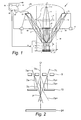
- Fig. 1 shows a simplified schematic drawing of an embodiment of a charged particle multi-beamlet lithography system 1.
- lithography system is for example described in U.S. patent Nos. 6,897,458 and 6, 958,804 and 7.084,414 and 7,129,502 , which are assigned to the applicant of the present application.
- Such lithography system 1 suitably comprises a beamlet generator generating a plurality of beamlets, a beamlet modulator patterning the beamlets to form modulated beamlets, and a beamlet projector for projecting the modulated beamlets onto a surface of a target.
- the beamlet generator typically comprises a source and at least one beam splitter.
- the source in FIG. 1 is an electron source 3 arranged to produce a substantially homogeneous, expanding electron beam 4.
- the beam energy of the electron beam 4 is preferably maintained relatively low in the range of about 1 to 10 keV.
- the acceleration voltage is preferably low, and the electron source 3 may be kept at a voltage between about -1 to -10 kV with respect to the target at ground potential, although other settings may also be used.
- the electron beam 4 from the electron source 3 passes a collimator lens 5 for collimating the electron beam 4.
- the collimator lens 5 may be any type of collimating optical system.
- the electron beam 4 may pass a double octopole (not shown).
- the electron beam 4 impinges on a beam splitter, in the embodiment of FIG. 1 an aperture array 6.
- the aperture array 6 preferably comprises a plate having through-holes.
- the aperture array 6 is arranged to block part of the beam 4. Additionally, the array 6 allows a plurality of beamlets 7 to pass through so as to produce a plurality of parallel electron beamlets 7.
- the lithography system 1 of FIG. 1 generates a large number of beamlets 7, preferably about 10,000 to 1,000,000 beamlets, although it is of course possible that more or less beamlets are generated. Note that other known methods may also be used to generate collimated beamlets.
- a second aperture array may be added in the system, so as to create subbeams from the electron beam 4 and to create electron beamlets 7 from the subbeam. This allows for manipulation of the subbeams further downstream, which turns out beneficial for the system operation, particularly when the number of beamlets in the system is 5,000 or more.
- the beamlet modulator typically comprises a beamlet blanker array 9 comprising an arrangement of a plurality of blankers, and a beamlet stop array 10.
- the blankers are capable of deflecting one or more of the electron beamlets 7.
- the blankers are more specifically electrostatic deflectors provided with a first electrode, a second electrode and an aperture. The electrodes are then located on opposing sides of the aperture for generating an electric field across the aperture.
- the second electrode is a ground electrode, i.e. an electrode connected to ground potential.
- the lithography system may further comprise a condenser lens array (not shown).
- the beamlet stop array 10 comprises an array of apertures for allowing beamlets to pass through.
- the beamlet stop array 10 in its basic form, comprises a substrate provided with through-holes, typically round holes although other shapes may also be used.
- the substrate of the beamlet stop array 10 is formed from a silicon wafer with a regularly spaced array of through-holes, and may be coated with a surface layer of a metal to prevent surface charging.
- the metal is of a type that does not form a native-oxide skin, such as CrMo.
- the beamlet blanker array 9 and the beamlet stop array 10 operate together to block or let pass the beamlets 7.
- the apertures of the beamlet stop array 10 are aligned with the apertures of the electrostatic deflectors in the beamlet blanker array 9. If beamlet blanker array 9 deflects a beamlet, it will not pass through the corresponding aperture in the beamlet stop array 10. Instead the beamlet will be blocked by the substrate of beamlet block array 10. If beamlet blanker array 9 does not deflect a beamlet, the beamlet will pass through the corresponding aperture in the beamlet stop array 10.
- cooperation between the beamlet blanker array 9 and the beamlet stop array 10 is such that deflection of a beamlet by a deflector in the blanker array 9 results in passage of the beamlet through the corresponding aperture in the beamlet stop array 10, while non-deflection results in blockage by the substrate of the beamlet stop array 10.
- the modulation system 8 is arranged to add a pattern to the beamlets 7 on the basis of input provided by a control unit 60.
- the control unit 60 may comprise a data storage unit 61, a read out unit 62 and data converter 63.
- the control unit 60 may be located remote from the rest of the system, for instance outside the inner part of a clean room.
- modulated light beams 14 holding pattern data may be transmitted to a projector 65 which projects light from the ends of fibers within a fiber array (schematically depicted as plate 15 ) into the electron optical portion of the lithography system 1, schematically denoted by the dashed box and reference number 18.
- the modulated light beams are projected on to the beamlet blanker array 9. More particularly, the modulated light beams 14 from optical fiber ends are projected on corresponding light sensitive elements located on the beamlet blanker array 9.
- the light sensitive elements may be arranged to convert the light signal into a different type of signal, for example an electric signal.
- a modulated light beam 14 carries a portion of the pattern data for controlling one or more blankers that are coupled to a corresponding light sensitive element.
- optical elements such as a projector 65 may be used.
- a mirror may be included, for example suitably placed between a projector 65 and the beamlet blanker array 9.
- the projector 65 may be appropriately aligned with the plate 15 by a projector positioning device 17 under control of the control unit 60.
- the distance between the projector 65 and the light sensitive elements within the light sensitive element may vary as well.
- the light beams may, at least partially, be transferred from the plate towards the light sensitive elements by means of an optical waveguide.
- the optical waveguide may guide the light to a position very close to the light sensitive elements, suitably less than a centimeter, preferably in the order of a millimeter away.
- a short distance between an optical waveguide and a corresponding light sensitive elements reduces light loss.
- the use of plate 15 and a projector 65 located away from the space that may be occupied by the charged particle beamlets has the advantage that the beamlet disturbance is minimized, and the construction of the beamlet blanker array 9 is less complex.
- the modulated beamlets coming out of the beamlet modulator are projected as a spot onto a target surface 13 of a target 24 by the beamlet projector.
- the beamlet projector typically comprises a scanning deflector for scanning the modulated beamlets over the target surface 13 and a projection lens system for focusing the modulated beamlets onto the target surface 13. These components may be present within a single end module.
- Such end module is preferably constructed as an insertable, replaceable unit.
- the end module may thus comprise a deflector array 11, and a projection lens arrangement 12.
- the insertable, replaceable unit may also include the beamlet stop array 10 as discussed above with reference to the beamlet modulator.
- the beamlets 7 After leaving the end module, the beamlets 7 impinge on a target surface 13 positioned at a target plane.
- the target usually comprises a wafer provided with a charged-particle sensitive layer or resist layer.
- the deflector array 11 may take the form of a scanning deflector array arranged to deflect each beamlet 7 that passed the beamlet stop array 10.
- the deflector array 11 may comprise a plurality of electrostatic deflectors enabling the application of relatively small driving voltages. Although the deflector array 11 is drawn upstream of the projection lens arrangement 12, the deflector array 11 may also be positioned between the projection lens arrangement 12 and the target surface 13.
- the projection lens arrangement 12 is arranged to focus the beamlets 7, before or after deflection by the deflector array 11. Preferably, the focusing results a geometric spot size of about 10 to 30 nanometers in diameter. In such preferred embodiment, the projection lens arrangement 12 is preferably arranged to provide a demagnification of about 100 to 500 times, most preferably as large as possible, e.g. in the range 300 to 500 times. In this preferred embodiment, the projection lens arrangement 12 may be advantageously located close to the target surface 13.
- a beam protector (not shown) may be located between the target surface 13 and the projection lens arrangement 12.
- the beam protector may be a foil or a plate provided with a plurality of suitably positioned apertures.
- the beam protector is arranged to absorb the released resist particles before they can reach any of the sensitive elements in the lithography system 1.
- the projection lens arrangement 12 may thus ensure that the spot size of a single pixel on the target surface 13 is correct, while the deflector array 11 may ensure by appropriate scanning operations that the position of a pixel on the target surface 13 is correct on a microscale.
- the operation of the deflector array 11 is such that a pixel fits into a grid of pixels which ultimately constitutes the pattern on the target surface 13. It will be understood that the macroscale positioning of the pixel on the target surface 13 is suitably enabled by a wafer positioning system present below the target 24.
- the target surface 13 comprises a resist film on top of a substrate.
- Portions of the resist film will be chemically modified by application of the beamlets of charged particles, i.e. electrons.
- the irradiated portion of the film will be more or less soluble in a developer, resulting in a resist pattern on a wafer.
- the resist pattern on the wafer can subsequently be transferred to an underlying layer, i.e. by implementation, etching and/or deposition steps as known in the art of semiconductor manufacturing.
- the irradiation is not uniform, the resist may not be developed in a uniform manner, leading to mistakes in the pattern.
- High-quality projection is therefore relevant to obtain a lithography system that provides a reproducible result. No difference in irradiation ought to result from deflection steps.
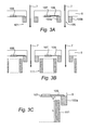
- FIG. 2 schematically shows the operation of an embodiment of the beamlet blanker array 9 in the lithography system of FIG. 1 .
- FIG. 2 schematically shows a cross-sectional view of a portion of a beamlet modulator comprising a beamlet blanker array 9 and beamlet stop array 10.
- the beamlet blanker array 9 is provided with a plurality of apertures.
- the target 24 has also been indicated. The figure is not drawn to scale.
- the shown portion of the beamlet modulator is arranged to modulate three beamlets 7a, 7b, and 7c.
- the beamlets 7a, 7b, 7c may form part of a single group of beamlets that may be generated from a beam originating from a single source or from a single subbeam.
- the beamlet modulator of FIG. 2 is arranged for converging groups of beamlets towards a common point of convergence P for each group. This common point of convergence P is preferably located on an optical axis O for the group of beamlets.
- beamlets 7a, 7b, 7c have an incident angle extending between the beamlet and the optical axis O.
- the orientation of beamlet 7b is substantially parallel to the optical axis.
- the direction of beamlet deflection to establish blocking of deflected beamlets by the substrate of the beamlet stop array 10 may be different for each beamlet.
- Beamlet 7a is blocked by deflection towards the left, i.e. towards the "-"-direction in FIG. 2 , indicated by dashed line 7a-.
- Beamlets 7b, 7c on the other hand are to be deflected towards the right, i.e. towards the "+"-direction, to established blocking of the respective beamlets.
- dashed lines 7b+ and 7c+ These blocking directions are indicated by dashed lines 7b+ and 7c+ respectively. Note that the choice of deflection direction may not be arbitrary. For example, for beamlet 7a, dashed line 7a+ shows that deflection of beamlet 7a towards the right would result in passage through the beamlet stop array 10. Therefore, deflection of beamlet 7a along line 7a+ would be inappropriate. On the other hand, deflection of beamlet 7b towards the left, indicated by dashed line 7b-, would be an option.
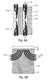
- FIG. 3A schematically shows a cross-sectional view of a portion of a beamlet blanker array 9 that may be used in the lithography system of FIG. 1 .
- the beamlet blanker array 9 comprises a plurality of modulators 101.
- a modulator comprises a first electrode 103a, a second electrode 103b, and an aperture 105.
- the electrodes 103a, 103b are located on opposing sides of the aperture 105 for generating an electric field across the aperture.
- a light sensitive element 107 is arranged to receive pattern data carrying light beams (not shown).
- the light sensitive element 107 is electrically connected to one or more modulators 101 via an electrical connection 109.
- the light sensitive element 107 receives pattern data via the light beams, converts the light signal into an electrical signal and then forwards the received and converted pattern data via the electrical connection 109 towards the one or more connected modulators 101.
- the one or more modulators 101 then modulate passing charged particle beamlets, such as electron beamlets 7 in accordance with the received pattern data.
- the light sensitive element 107 may be provided with an anti-reflection coating 108 to reduce background radiation caused by reflected light, which may disturb a correct readout of the data carried by the light beam.
- Modulation of the beamlets is thus based on controlling the application of an electric field across the apertures within the beamlet blanker array 9.
- practical use of a lithography system such as the one presented in FIG. 1 shows that effective modulation is not always possible.
- the light sensitive elements 107 may act as electric field sources due to a collection of scattered electrons on their surface. This may particularly be the case if a anti-reflection coating such as coating 108 in FIGS. 3A, 3B is used.
- the anti-reflection coating is generally electrically insulating, which results in a relatively fast collection of scattered charged particles.
- components that are used to transfer the light towards the light sensitive elements for example optical fibers, may collect charged particles as well, in particular if they are not completely coated with a conductive coating.
- FIG. 3B schematically shows a cross-sectional view of a portion of a beamlet blanker array 9 provided with a shielding structure 111 according to an embodiment of the invention.
- the shielding structure 111 is an electrically conductive structure, and is arranged to shield electric fields and/or magnetic fields generated in proximity of the light sensitive elements 107, for example on top of an electrically insulating layer that may cover the light sensitive elements 107 for protection and/or anti-reflection purposes, from the modulators 105.
- references to the expression "electric field” should be understood to mean electric and/or magnetic field.
- the shielding structure 111 reduces, and preferably eliminates, the interfering of additional electric fields with the fields generated by the modulators 101.
- the reduction or elimination of electric field interference results in more accurate and robust modulation of the charged particle beamlets 7 by the modulators 101.
- the shielding structure 111 is kept at a predetermined electric potential.
- the shielding structure 111 is connected to ground potential.
- the shielding structure is not necessarily in contact with the beamlet blanker array 9.
- the purpose of the shielding structure 111 is to stop the electric fields generated in proximity of the light sensitive elements 107. Note that a fixed connection of the shielding structure 111 with the beamlet blanker array 9 is not essential to achieve such purpose.
- FIG. 3C schematically shows a cross-sectional view of a portion of the blanker array of FIG. 3B .
- FIG. 3C illustrates the ratio between the height h of the shielding structure 111 and the distance d between a light sensitive element 107 and the perpendicular projection of the shielding structure 111 onto the beamlet blanker array 9.
- the distance d will hereinafter be referred to as lateral shielding distance.
- the height h is at least about the same as the lateral shielding distance d.
- Such dimensions allow to effectively shield the electric fields generated in proximity of the light sensitive elements.
- the height h is more than about 2.5 times the lateral shielding distance d , the influence of electric fields generated in proximity of the light sensitive elements on the operation of the modulators is negligible.
- FIG. 4 schematically shows a top view of a lay-out of a beamlet blanker array 9 that may be used in embodiments of the invention.
- the beamlet blanker array 9 shown in FIG. 4 is divided into beam areas 121 and non-beam areas 122. Although the width of the beam areas 121 and non-beam areas 122 are shown to be about the same, this is not essential. The dimensions of the areas may differ based on the layout used.
- the beam areas 121 include one or more modulators for modulating beamlets.
- the non-beam areas 122 include one or more light sensitive elements.
- the use of beam areas 121 and non-beam areas 122 in an optical column in a maskless lithography system has the advantage that the density of modulators and light sensitive area can be increased.
- FIG. 5 schematically shows the beamlet blanker array of FIG. 4 provided with a shielding structure 111 according to an embodiment of the invention.
- the shielding structure 111 that is at least its projection in a direction substantially perpendicular to the beamlet blanker array surface, is located between the light sensitive elements within the non-beam areas 122 and the modulators within the beam areas 121.
- the shielding structure 111 is arranged to substantially shield electric fields generated in proximity of the light sensitive elements.
- the shielding structure 111 of FIG. 5 can be described as comprising side walls forming an open-ended box-like structure.
- the side walls may be integrated into a single body, for example by connection to an additional structure 111'.
- a single body has the benefit of an increased mechanical robustness.
- the structure 111, 111' may be handled more easily. Integration of different components to form the shielding structure 111, 111' may be executed by adding the portions 111' to the separate walls forming the functional shielding structure 111, for example by welding. Alternatively, the shielding structure may be manufactured out of one piece, for example by using techniques such as electrical discharge machining. Yet another way of creating an integrated shielding structure 111, 111' is to attach different components to a supporting substrate. This substrate may be the beamlet blanker array 9 or a component thereof, but may also be a separate suitable substrate.
- the shielding structure 111 is not necessarily physically connected to the beamlet blanker array 9. If located within sufficiently close distance of the beamlet blanker array 9 the shielding structure 111 can still sufficiently shield electric fields.
- the shielding structure 111 further includes a portion 111'.
- This additional portion 111' can provide mechanical support to the shielding structure 111.
- the additional portion 111' is arranged to shield electric and/or magnetic fields originating from other potentially disturbing electric field generating sources, such as electricity cables.
- Materials suitable for the shielding structure 111 are materials with sufficiently high electric conductivity. Additionally, the material should have sufficient strength and workability.
- An exemplary suitable material for use as main component of the shielding structure is titanium (Ti).
- Other exemplary materials that may be used include molybdenum (Mo) and aluminum (Al).
- the shielding structure is made using Ti-plates coated with Mo.
- the shielding structure includes a stack of Mo sheets with Al spacers.
- light beams may be directed towards the light sensitive elements by using an optical fiber array.
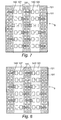
- FIG. 6A schematically shows an exemplary embodiment of an optical fiber arrangement 131 selectively placed over the beamlet blanker array 9 of FIG. 5 .
- the optical fiber arrangement 131 comprises a plurality of optical fibers 133 arranged to guide pattern data carrying light beams towards the light sensitive elements within the non-beam areas 122.
- the fibers 133 are positioned such that they do not hinder a passage of charged particle beamlets arranged to pass through the apertures within the beam area 121 of the beamlet blanker array 9.
- the exemplary optical fiber arrangement 131 of FIG. 6A comprises two portions per non-beam area 122.
- a first portion 131a comprises a number of fibers 133 that enter a space above the non-beam area 122 from one side, while the second portion 131b comprises a number of fibers 133 entering the space above the non-beam area 122 at an opposing side.
- the number of fibers 133 within each portion 131a, 131b may be equal to each other.
- the use of different portions allows for more space per fiber 133, and reduces the risk of damaging the fibers 133.
- FIG. 6B schematically shows a cross-sectional view of the arrangement shown in FIG. 6A along the line VIB-VIB'.
- the fibers 133 within the arrangement 131 terminate in a fiber array 135.
- the ends of the fibers within the fiber array 135 are directed towards the light sensitive elements (not shown) within the non-beam area of the beamlet blanker array 9.
- the fiber array 135 is preferably placed in close proximity of the surface of the beamlet blanker array 9 to minimize alignment errors due to poorly oriented fibers 133 within the fiber array 135.
- one or more small openings 137 in the wall 111' are provided to allow the introduction of the fibers within this enclosure.
- the cross-sectional area of these openings 137 is preferably as small as possible.
- the use of portions may help to reduce the dimensions of the cross-sectional area in a direction substantially perpendicular to the surface of the fiber array.
- the cross-sectional area of the openings 137 may be chosen somewhat larger.
- FIG. 6C schematically shows a more detailed view of alignment of the optical fiber arrangement of FIGS. 6A, 6B .
- the fibers 133 within the fiber array 135 are substantially aligned with corresponding light sensitive elements 107 located in the non-beam area of the beamlet blanker array 9.
- the fiber array 135 includes an array of microlenses 139.
- the use of microlenses 139 improves optical communication.
- the microlenses 139 are arranged to focus light leaving the respective fibers 133 onto the light sensitive element 107.
- the microlenses 139 thus reduce the spot size of the light beam at the light receiving surface of the light sensitive element 107.
- the use of microlenses alleviates alignment requirements between fiber array 135 and the light sensitive elements 107. A small deviation of the reduced spot size can still be handled by the light sensitive element because most, if not all, light leaving the respective fiber 133 still falls onto its light receiving surface.
- the fiber array 135 may be placed in close proximity of the light sensitive elements 107 to achieve communication with reduced light loss.
- Such embodiment has the advantage that it is less complex due to the absence of the microlenses 139.
- FIG. 7 schematically shows a top view of a topographic arrangement of a beamlet blanker array according to an embodiment of the invention.
- the beamlet blanker array 9 is again divided in beam areas 121 and non-beam areas 122.
- the beam areas 121 and the non-beam areas 122 are separated by walls forming a shielding structure 111 as discussed earlier.
- the beam areas 121 comprise a plurality of modulators 101.
- the non-beam areas 122 comprise a plurality of light sensitive elements 107. Suitable examples of the light sensitive elements 107 include but are not limited to photodiodes and phototransistors.
- the non-beam areas 122 further include demultiplexers 140.
- the light signals received by the light sensitive elements 107 are multiplexed signals which include information for more than one modulator 101.
- a signal received by a light sensitive element 107 is transferred to a demultiplexer 140.
- the demultiplexer 140 demultiplexes the signal and forwards demultiplexed signals to the correct modulators 101 via dedicated electrical connections 142.
- the number of light sensitive elements 107 is lower than the number of modulators 101. Having a limited number of light sensitive elements 107 enables reduction of the dimensions of the non-beam areas 122.
- the beam areas 121 may then be placed more closely together to increase the number of modulators 101 per unit area in the blanker array 9. In comparison to a non-multiplexed embodiment the layout of the beamlet blanker array 9 would then be more compact if the same number of modulators 101 would be used. If the dimensions of the blanker array 9 would remain substantially the same, more modulators could be used.
- the use of a multiplexed embodiment as shown in FIG. 7 could enable the use of light sensitive elements 107 with a greater light receiving area.
- the use of a greater light receiving area per light sensitive element 107 reduces the complexity of the optics needed to direct the light signal towards the correct light sensitive elements 107 and may alleviate requirements related to the alignment of light beams and light sensitive elements 107.
- FIG. 8 schematically shows a top view of a topographic arrangement of a beamlet blanker array 9 according to an example.
- the shielding structure 111 now embraces a portion of the light sensitive elements 107 and the demultiplexers 142 within a non-beam area 122.
- This modular approach has the advantage that malfunctioning channels and/or components like demultiplexers 142 can be more easily corrected for.
- FIG. 9 schematically shows a top view of a topographic arrangement of a beamlet blanker array 9 according to yet another example.
- the shielding structure 111 now merely embraces the light sensitive elements 107 within a non-beam area 122.
- FIG. 10 schematically shows a cross-sectional view of a beamlet blanker array 9 with an embodiment of a shielding structure 111 using free space optics.
- the light beams 141 indicated herein with dashed-dotted arrows have an incident angle of approximately 90 degrees. Note that this is not essential.
- the particular embodiment of the shielding structure 111 shown in FIG. 10 includes a substrate 160 provided with side walls 161 extending thereon.
- the side walls 161 are located adjacent to apertures 165 within the substrate 160 that are aligned with one or more apertures 105 within the beamlets blanker array 9. Note that although the beamlets 7 in FIG. 10 pass the beamlet array 9 substantially perpendicular, this is not essential.
- the side walls 161 are suitably made of conductive material.
- a side wall 161 is arranged circumferentially around an aperture 165.
- a side wall 161 is arranged circumferentially around a lateral area defined by the one or more light sensitive elements 107.
- a structure of side walls 161 may be provided, including a side wall extending around the lateral area of light sensitive elements and a side wall extending around the aperture 165.
- the shielding structure 111 does not have to be sealed to the beamlet blanker array 9.
- the embodiment of the shielding structure 111 is in particular suitable for a topographical arrangement as schematically shown in FIG. 7 .
- the long extension of the side walls in one direction (in FIG. 7 a vertical direction), height requirements of the shielding structure 111 do not have a significant effect on the angle at which the data carrying light beams can be directed onto the light sensitive elements 107.
- the height of the shielding structure is substantially greater than the lateral shielding distance introducing the light from directions with a significant component substantially perpendicular to the direction of the walls forming the shielding structure limits the angle at which light can reach the light sensitive elements 107.
- the long extension of the shielded area in the direction of the side walls forming the shielding structure 111 now ensures that such limited possible entry of light beams only occurs if the beams originate from a direction with a significant component substantially perpendicular to the side wall orientation.
- the angles at which light can couple into the shielded area when incident from a direction substantially parallel to the side wall orientation may vary widely as no significant shielding is needed in these directions.
- the shielding structure 111 does not necessarily be physically connected to the beamlet blanker array 9. However, in some embodiments both structures are connected.
- FIG. 11 shows an embodiment in which the shielding structure 111 is connected to the blanker array 9 using solder balls 170.
- the solder balls 170 may extend through a passivation layer (not shown) that is commonly used in IC manufacturing.
- the use of such soldering connection may be particularly suitable for shielding structures 111 that embrace a relatively small area, for example in a topographical arrangements as shown in FIGS. 8 and 9 .
- the shielding structure 111 is a wall-like structure having a height that is at least similar in dimensions to the lateral shielding distance.
- a shielding structure 111 comprising a plate 171 with apertures 175.
- Some apertures are aligned with the apertures 105 within the beamlet blanker array 9 while others are aligned with the light sensitive elements 107 to allow illumination of these elements by the data carrying light beams (not shown).
- the embodiment shown in FIG. 11 includes a beamlet blanker array 9 provided with an interconnect structure 173 arranged to enable connection of light sensitive elements 107 at different levels with the electrostatic deflectors 103a, 103b of the modulators 105.
- Such multi-level connection structure may reduce the modulator pitch within the beamlet blanker array 9, which can result in a more compact design.
- the plate 171 may be physically connected to the beamlet blanker array 9, for example via solder balls 170, but may also be positioned at some distance, indicated in FIG. 11 by structure 171' provided with dashed contour lines. In such case, the beamlet blanker array 9 and the structure 171' may be connected to the same frame to ensure that both structures are suitably aligned with respect to each other.
- the distance between the structure 171' and the blanker array 9 may be suitably designed based on the desired extent of electric field shielding and the available angle for data carrying light beams to "hit" the light sensitive elements 107.
- the plate 171, 171' may be a metal piece in which the apertures are shaped by punching.
- An example of such piece is referred to in the semiconductor industry as a leadframe.
- the plate 171, 171' may take the form of a semiconductor or ceramic substrate provided with through-holes, for example made by using one or more suitable etching techniques.
- the direction of the charged particle beamlet 7 is not essential.
- the embodiment shown in FIG. 11 may also be used while a particle beamlet 7 passes through the aperture 105 in a substantially upward direction.
- Fig. 12 shows yet another beamlet blanker array 9 provided with a shielding structure 111.
- the beamlet blanker array 9 of this example comprises a first substrate 200 and a second substrate 201.
- the modulators with deflectors 103a, 103b are defined on the first substrate 200.
- the light sensitive elements 107 are defined at a surface of the second substrate 201.
- Solder balls 202 provide mechanical connections from the first substrate 200 to the second substrate 201 and electrical connections between the light sensitive elements 107 and the deflectors 103a, 103b, and/or any intermediate circuitry.
- Light beams 141 now arrive at the light sensitive elements 107 from an opposite direction, e.g. the top side of the column. Thereto, radiation apertures 205 are present in the first substrate 200.
- the shielding structure 111 is connected to the second substrate 201, and takes the form of side walls.
- the side walls may extend in a single direction (see e.g. topographic arrangement of FIG. 7 ) or may embrace one or more light sensitive elements 107 (see e.g. topographic arrangements of FIGS. 8 and 9 ).
Landscapes
- Chemical & Material Sciences (AREA)
- Engineering & Computer Science (AREA)
- Analytical Chemistry (AREA)
- Nanotechnology (AREA)
- Physics & Mathematics (AREA)
- Crystallography & Structural Chemistry (AREA)
- Condensed Matter Physics & Semiconductors (AREA)
- General Physics & Mathematics (AREA)
- Manufacturing & Machinery (AREA)
- Mathematical Physics (AREA)
- Theoretical Computer Science (AREA)
- Electron Beam Exposure (AREA)
Claims (14)
- Dispositif de modulation (8) pour une utilisation dans un système de lithographie à multiples mini-faisceaux de particules chargées (1), le dispositif de modulation (8) comprenant :- un réseau de suppresseurs de mini-faisceaux (9) pour configurer une pluralité de mini-faisceaux (7) selon un motif, dans lequel le réseau de suppresseurs de mini-faisceaux (9) comprend une pluralité de modulateurs (101) et une pluralité d'éléments photosensibles (107), les éléments photosensibles (107) étant agencés pour recevoir des faisceaux lumineux porteurs de données de motif (14, 141) et convertir les faisceaux lumineux en signaux électriques, l'élément photosensible (107) étant connecté électriquement à un ou plusieurs modulateurs (101) pour fournir les données de motif reçues aux un ou plusieurs modulateurs (101) ;caractérisé en ce que le dispositif de modulation comprend en outre :
dans lequel le réseau de suppresseurs de mini-faisceaux (9) comprend un substrat pourvu d'une première zone (121) comprenant au moins un modulateur (101) et d'une seconde zone (122) exempte de modulateurs et comportant un ou plusieurs éléments photosensibles (107) ;- une structure de protection (111) d'un matériau conducteur d'électricité agencé pour protéger sensiblement les champs électriques générés à proximité des éléments photosensibles (107) des modulateurs (101), dans lequel la structure de protection (111) est agencée pour être réglée à un potentiel prédéterminé ;et en ce que la projection de la structure de protection (111) sur le réseau de suppresseurs de mini-faisceaux (9) forme une limite entre les première et seconde zones, protégeant ainsi les modulateurs des champs électriques générés à proximité des éléments photosensibles. - Dispositif selon la revendication 1, dans lequel un modulateur de la pluralité de modulateurs (101) comprend une première électrode (103a), une seconde électrode (103b) et une ouverture (105), les électrodes étant situées sur des côtés opposés de l'ouverture (105) pour générer un champ électrique en travers de l'ouverture (105).
- Dispositif selon la revendication 2, dans lequel la première zone (121) et la seconde zone (122) prennent la forme de bandes adjacentes et la structure de protection (111) comprend une paroi ayant une longueur et une hauteur et une projection de la structure de protection (111) sur la surface de substrat du réseau de suppresseurs de mini-faisceaux (9) dans une direction sensiblement parallèle à la hauteur de paroi et sensiblement perpendiculaire à la longueur de paroi sépare la première zone (212) de la seconde zone (122).
- Dispositif selon l'une quelconque des revendications 1 à 3, dans lequel la structure de protection (111) comprend des parois latérales formant une structure de type caisson ouverte aux extrémités.
- Dispositif selon la revendication 4, dans lequel une première extrémité de la structure de type caisson ouverte aux extrémités est tournée vers la surface de substrat du réseau de suppresseurs de mini-faisceaux (9) et une seconde extrémité opposée de la structure de type caisson ouverte aux extrémités est tournée à l'opposé du réseau de suppresseurs de mini-faisceaux (9).
- Dispositif selon la revendication 5, dans lequel la seconde extrémité est pourvue d'un couvercle fermant sensiblement la seconde extrémité.
- Dispositif selon l'une quelconque des revendications 4 à 6, dans lequel le volume enserré par la structure de protection comprend un ou plusieurs éléments optiques pour guider les faisceaux lumineux porteurs de données de motif (14, 141) vers les éléments photosensibles (107).
- Dispositif selon la revendication 7, dans lequel les un ou plusieurs éléments optiques comprennent un réseau de fibres optiques (135).
- Dispositif selon l'une quelconque des revendications 4 à 8, dans lequel au moins l'une des parois latérales est agencée pour introduire les faisceaux lumineux porteurs de données de motif (14, 141) dans le volume enserré par la structure de protection (111).
- Dispositif selon la revendication 9, dans lequel au moins l'une des parois latérales de la structure de protection (111) comprend une ouverture pour recevoir l'entrée de fibres optiques (133) dans le volume enserré par la structure de protection (111).
- Dispositif selon la revendication 9, dans lequel au moins l'une des parois latérales de la structure de protection (111) comprend une partie qui est transparente pour la lumière des faisceaux lumineux porteurs de données de motif (14, 141).
- Dispositif selon l'une quelconque des revendications 4 à 11, dans lequel le rapport entre la hauteur de la structure de protection (111) et la distance entre un élément photosensible (107) et la projection perpendiculaire de la paroi latérale la plus proche de la structure de protection (111) sur le réseau de suppresseurs de mini-faisceaux (9) est supérieur à environ 1, de préférence supérieur à environ 2,5.
- Système de lithographie à multiples mini-faisceaux de particules chargées (1) pour transférer un motif sur la surface d'une cible (13) en utilisant une pluralité de mini-faisceaux de particules chargées, le système comprenant :- un générateur de faisceaux (3, 4, 5) pour générer une pluralité de mini-faisceaux de particules chargées (7) ;- un dispositif de modulation (8) selon l'une quelconque des revendications 1 à 12 ; et- un système de projection (12) pour projeter les mini-faisceaux à motif sur la surface cible (13).
- Procédé de modulation de mini-faisceaux de particules chargées (7) dans un système de lithographie à multiples mini-faisceaux de particules chargées (1) pour transférer un motif à une surface cible (13), le procédé comprenant :- la fourniture d'un réseau de suppresseurs de mini-faisceaux (9) comprenant une pluralité de modulateurs (101) et une pluralité d'éléments photosensibles (107), les éléments photosensibles (107) étant agencés pour recevoir des faisceaux lumineux porteurs de données de motif (14, 141) et étant connectés électriquement à un ou plusieurs modulateurs pour fournir les données de motif reçues, et les modulateurs comprenant une première électrode (103a), une seconde électrode (103b) et une ouverture (105), dans lequel les électrodes sont situées sur des côtés opposés des ouvertures pour générer un champ électrique en travers de l'ouverture (105),
ledit réseau de suppresseurs de mini-faisceaux (9) comprenant en outre une structure de protection (111) d'un matériau conducteur d'électricité pour protéger sensiblement les champs électriques générés par les modulateurs pour moduler les mini-faisceaux de champs électriques générés à proximité des éléments photosensibles (107), dans lequel la structure de protection (111) est agencée pour être réglée à un potentiel prédéterminé,
et dans lequel le réseau de suppresseurs de mini-faisceaux (9) comprend un substrat pourvu d'une première zone (121) comprenant au moins un modulateur (101) et d'une seconde zone (122) exempte de modulateurs et comportant un ou plusieurs éléments photosensibles (107), et dans lequel la projection de la structure de protection (111) sur le réseau de suppresseurs de mini-faisceaux (9) forme une limite entre les première et seconde zones ;
la transmission de données de motif au réseau de suppresseurs de mini-faisceaux ;
et- la modulation de mini-faisceaux passant à travers le réseau de suppresseurs de mini-faisceaux selon les données de motif reçues,dans lequel la modulation des mini-faisceaux est réalisée en utilisant un champ électrique sensiblement exempt de contributions généré à proximité des éléments photosensibles (107).
Applications Claiming Priority (2)
| Application Number | Priority Date | Filing Date | Title |
|---|---|---|---|
| US25477909P | 2009-10-26 | 2009-10-26 | |
| PCT/EP2010/066198 WO2011051304A1 (fr) | 2009-10-26 | 2010-10-26 | Dispositif de modulation et système de lithographie à multiples petits faisceaux de particules chargées l'utilisant |
Publications (2)
| Publication Number | Publication Date |
|---|---|
| EP2494580A1 EP2494580A1 (fr) | 2012-09-05 |
| EP2494580B1 true EP2494580B1 (fr) | 2016-10-19 |
Family
ID=43500320
Family Applications (3)
| Application Number | Title | Priority Date | Filing Date |
|---|---|---|---|
| EP10773617.5A Active EP2494579B1 (fr) | 2009-10-26 | 2010-10-26 | Système de lithographie à multiples petits faisceaux de particules chargées, dispositif de modulation et procédé de fabrication de celui-ci |
| EP10773044.2A Active EP2494578B1 (fr) | 2009-10-26 | 2010-10-26 | Système de lithographie à multiples petits faisceaux de particules chargées, avec dispositif de modulation |
| EP10773891.6A Active EP2494580B1 (fr) | 2009-10-26 | 2010-10-26 | Dispositif de modulation et système de lithographie à multiples petits faisceaux de particules chargées l'utilisant |
Family Applications Before (2)
| Application Number | Title | Priority Date | Filing Date |
|---|---|---|---|
| EP10773617.5A Active EP2494579B1 (fr) | 2009-10-26 | 2010-10-26 | Système de lithographie à multiples petits faisceaux de particules chargées, dispositif de modulation et procédé de fabrication de celui-ci |
| EP10773044.2A Active EP2494578B1 (fr) | 2009-10-26 | 2010-10-26 | Système de lithographie à multiples petits faisceaux de particules chargées, avec dispositif de modulation |
Country Status (8)
| Country | Link |
|---|---|
| US (4) | US8492731B2 (fr) |
| EP (3) | EP2494579B1 (fr) |
| JP (3) | JP5781523B2 (fr) |
| KR (3) | KR20120098756A (fr) |
| CN (3) | CN102687233B (fr) |
| NL (2) | NL2005584C2 (fr) |
| TW (2) | TWI498937B (fr) |
| WO (3) | WO2011051304A1 (fr) |
Families Citing this family (42)
| Publication number | Priority date | Publication date | Assignee | Title |
|---|---|---|---|---|
| US8258484B2 (en) * | 2008-04-15 | 2012-09-04 | Mapper Lithography Ip B.V. | Beamlet blanker arrangement |
| US9341936B2 (en) | 2008-09-01 | 2016-05-17 | D2S, Inc. | Method and system for forming a pattern on a reticle using charged particle beam lithography |
| EP2494579B1 (fr) * | 2009-10-26 | 2017-08-02 | Mapper Lithography IP B.V. | Système de lithographie à multiples petits faisceaux de particules chargées, dispositif de modulation et procédé de fabrication de celui-ci |
| US9070851B2 (en) | 2010-09-24 | 2015-06-30 | Seoul Semiconductor Co., Ltd. | Wafer-level light emitting diode package and method of fabricating the same |
| KR101725299B1 (ko) * | 2010-10-26 | 2017-04-10 | 마퍼 리쏘그라피 아이피 비.브이. | 변조 디바이스 및 이를 사용하는 하전 입자 멀티-빔렛 리소그래피 시스템 |
| JP5679774B2 (ja) * | 2010-11-09 | 2015-03-04 | キヤノン株式会社 | 偏向器アレイ、荷電粒子描画装置、デバイス製造方法、偏向器アレイの製造方法 |
| NL2007604C2 (en) * | 2011-10-14 | 2013-05-01 | Mapper Lithography Ip Bv | Charged particle system comprising a manipulator device for manipulation of one or more charged particle beams. |
| NL2006868C2 (en) * | 2011-05-30 | 2012-12-03 | Mapper Lithography Ip Bv | Charged particle multi-beamlet apparatus. |
| JP2013182945A (ja) * | 2012-02-29 | 2013-09-12 | Canon Inc | 描画装置および物品製造方法 |
| JP2015511069A (ja) * | 2012-03-19 | 2015-04-13 | ケーエルエー−テンカー コーポレイション | 柱で支持されたマイクロ電子レンズアレイ |
| US9343267B2 (en) | 2012-04-18 | 2016-05-17 | D2S, Inc. | Method and system for dimensional uniformity using charged particle beam lithography |
| WO2013158573A1 (fr) | 2012-04-18 | 2013-10-24 | D2S, Inc. | Procédé et système de formation de motifs par utilisation de lithographie par faisceau de particules chargées |
| NL2010759C2 (en) | 2012-05-14 | 2015-08-25 | Mapper Lithography Ip Bv | Modulation device and power supply arrangement. |
| JP2014007013A (ja) * | 2012-06-22 | 2014-01-16 | Canon Inc | 静電レンズアレイ、マルチ荷電粒子光学系、及びフォーカス調整方法 |
| WO2015090378A1 (fr) * | 2013-12-18 | 2015-06-25 | Mapper Lithography Ip Bv | Dispositif de modulation et système de lithographie comprenant un tel dispositif |
| JP5816739B1 (ja) * | 2014-12-02 | 2015-11-18 | 株式会社ニューフレアテクノロジー | マルチビームのブランキングアパーチャアレイ装置、及びマルチビームのブランキングアパーチャアレイ装置の製造方法 |
| JP6426489B2 (ja) * | 2015-02-03 | 2018-11-21 | 東京エレクトロン株式会社 | エッチング方法 |
| JP2017168574A (ja) * | 2016-03-15 | 2017-09-21 | 株式会社ニューフレアテクノロジー | マルチ荷電粒子ビームのブランキング装置、マルチ荷電粒子ビームのブランキング方法、及びマルチ荷電粒子ビーム描画装置 |
| US9981293B2 (en) | 2016-04-21 | 2018-05-29 | Mapper Lithography Ip B.V. | Method and system for the removal and/or avoidance of contamination in charged particle beam systems |
| NL2019503B1 (en) | 2016-09-08 | 2018-08-31 | Mapper Lithography Ip Bv | Fabricating unique chips using a charged particle multi-beamlet lithography system |
| US10714427B2 (en) | 2016-09-08 | 2020-07-14 | Asml Netherlands B.V. | Secure chips with serial numbers |
| US10418324B2 (en) | 2016-10-27 | 2019-09-17 | Asml Netherlands B.V. | Fabricating unique chips using a charged particle multi-beamlet lithography system |
| WO2018117275A1 (fr) | 2016-12-23 | 2018-06-28 | Mapper Lithography Ip B.V. | Fabrication de puces uniques à l'aide d'un système de lithographie à petits faisceaux multiples de particules chargées |
| JP6720861B2 (ja) * | 2016-12-28 | 2020-07-08 | 株式会社ニューフレアテクノロジー | マルチビーム用アパーチャセット及びマルチ荷電粒子ビーム描画装置 |
| US10840056B2 (en) * | 2017-02-03 | 2020-11-17 | Kla Corporation | Multi-column scanning electron microscopy system |
| WO2018197169A1 (fr) | 2017-04-28 | 2018-11-01 | Asml Netherlands B.V. | Appareil utilisant de multiples faisceaux de particules chargées |
| KR102649183B1 (ko) * | 2017-10-02 | 2024-03-21 | 에이에스엠엘 네델란즈 비.브이. | 하전 입자 빔들을 사용하는 장치 |
| JP6966958B2 (ja) * | 2018-03-01 | 2021-11-17 | 株式会社荏原製作所 | めっき液を撹拌するために用いるパドルおよびパドルを備えるめっき装置 |
| JP6847886B2 (ja) * | 2018-03-20 | 2021-03-24 | 株式会社東芝 | 荷電粒子ビーム偏向デバイス |
| WO2019211072A1 (fr) * | 2018-05-01 | 2019-11-07 | Asml Netherlands B.V. | Appareil d'injection à faisceaux multiples |
| JP6965222B2 (ja) * | 2018-09-14 | 2021-11-10 | 株式会社東芝 | 半導体装置 |
| WO2020141031A1 (fr) * | 2018-12-31 | 2020-07-09 | Asml Netherlands B.V. | Appareil d'inspection à faisceaux multiples |
| DE102019005362A1 (de) * | 2019-07-31 | 2021-02-04 | Carl Zeiss Multisem Gmbh | Verfahren zum Betreiben eines Vielzahl-Teilchenstrahlsystems unter Veränderung der numerischen Apertur, zugehöriges Computerprogrammprodukt und Vielzahl-Teilchenstrahlsystem |
| US11120965B2 (en) | 2019-12-04 | 2021-09-14 | ICT Integrated Circuit Testing Gesellschaft für Halbleiterprüftechnik mbH | Beam blanking device for a multi-beamlet charged particle beam apparatus |
| JP7359050B2 (ja) * | 2020-03-18 | 2023-10-11 | 株式会社ニューフレアテクノロジー | マルチビーム用のブランキング装置及びマルチ荷電粒子ビーム描画装置 |
| WO2022135926A1 (fr) * | 2020-12-23 | 2022-06-30 | Asml Netherlands B.V. | Lentille électronique |
| NL2027746B1 (en) * | 2021-03-12 | 2022-09-29 | Elstar Dynamics Patents B V | Dynamic glazing comprising a substrate with interlaced mesh electrodes |
| TWI886395B (zh) * | 2021-06-14 | 2025-06-11 | 日商紐富來科技股份有限公司 | 多帶電粒子束描繪裝置 |
| EP4170695A1 (fr) | 2021-10-19 | 2023-04-26 | ASML Netherlands B.V. | Ensemble détecteur, dispositif de particules chargées, appareil et procédés |
| KR20240093780A (ko) | 2021-10-19 | 2024-06-24 | 에이에스엠엘 네델란즈 비.브이. | 검출기 조립체, 하전 입자 디바이스, 장치, 및 방법 |
| WO2023117191A1 (fr) | 2021-12-24 | 2023-06-29 | Elstar Dynamics Patents B.V. | Substrat comprenant des électrodes et modulateur de lumière à diffraction réduite |
| JP2024030513A (ja) * | 2022-08-24 | 2024-03-07 | 株式会社ニューフレアテクノロジー | ビーム検出器、マルチ荷電粒子ビーム照射装置、及びビーム検出器の調整方法 |
Family Cites Families (35)
| Publication number | Priority date | Publication date | Assignee | Title |
|---|---|---|---|---|
| JPS554011A (en) * | 1978-06-22 | 1980-01-12 | Nippon Telegr & Teleph Corp <Ntt> | Optical branching and receiving device |
| JP3145149B2 (ja) * | 1991-10-17 | 2001-03-12 | 富士通株式会社 | 荷電粒子ビーム偏向装置 |
| US5719416A (en) * | 1991-12-13 | 1998-02-17 | Symetrix Corporation | Integrated circuit with layered superlattice material compound |
| DE4241045C1 (de) | 1992-12-05 | 1994-05-26 | Bosch Gmbh Robert | Verfahren zum anisotropen Ätzen von Silicium |
| GB9316280D0 (en) * | 1993-08-05 | 1993-09-22 | Capteur Sensors & Analysers | Gas sensors |
| JP3311927B2 (ja) * | 1996-04-18 | 2002-08-05 | トヨタ自動車株式会社 | 光−磁気光学効果測定装置 |
| JP4246401B2 (ja) * | 2001-01-18 | 2009-04-02 | 株式会社アドバンテスト | 電子ビーム露光装置及び電子ビーム偏向装置 |
| KR100385228B1 (ko) * | 2001-04-18 | 2003-05-27 | 삼성전자주식회사 | 불휘발성 메모리를 프로그램하는 방법 및 장치 |
| JP4248191B2 (ja) * | 2002-04-10 | 2009-04-02 | キヤノン株式会社 | アレイ構造体の製造方法 |
| US6818911B2 (en) * | 2002-04-10 | 2004-11-16 | Canon Kabushiki Kaisha | Array structure and method of manufacturing the same, charged particle beam exposure apparatus, and device manufacturing method |
| JP4222927B2 (ja) | 2002-09-20 | 2009-02-12 | エーエスエムエル ネザーランズ ビー.ブイ. | 少なくとも2波長を使用するリソグラフィ装置用アライメント・システム |
| EP2302457B1 (fr) * | 2002-10-25 | 2016-03-30 | Mapper Lithography Ip B.V. | Système de lithographie |
| CN101414534B (zh) * | 2002-10-30 | 2012-10-03 | 迈普尔平版印刷Ip有限公司 | 电子束曝光系统 |
| JP2004282038A (ja) | 2003-02-28 | 2004-10-07 | Canon Inc | 偏向器、偏向器を製造する方法、偏向器を適用した荷電粒子線露光装置 |
| KR101068607B1 (ko) | 2003-03-10 | 2011-09-30 | 마퍼 리쏘그라피 아이피 비.브이. | 복수 개의 빔렛 발생 장치 |
| ATE524822T1 (de) | 2003-05-28 | 2011-09-15 | Mapper Lithography Ip Bv | Belichtungsverfahren für strahlen aus geladenen teilchen |
| JP4387755B2 (ja) * | 2003-10-14 | 2009-12-24 | キヤノン株式会社 | 偏向器アレイおよびその製造方法、ならびに該偏向器アレイを用いた荷電粒子線露光装置 |
| US7394071B2 (en) * | 2004-12-20 | 2008-07-01 | Electronics And Telecommunications Research Institute | Micro column electron beam apparatus formed in low temperature co-fired ceramic substrate |
| JP4652829B2 (ja) * | 2005-01-26 | 2011-03-16 | キヤノン株式会社 | 電子線露光装置およびデバイス製造方法 |
| US20060204166A1 (en) * | 2005-03-14 | 2006-09-14 | Naugler W E Jr | Method and apparatus for monitoring and calibrating an emissive pixel |
| JP2007019248A (ja) * | 2005-07-07 | 2007-01-25 | Canon Inc | 偏向器、荷電粒子線露光装置およびデバイス製造方法 |
| JP2007019242A (ja) * | 2005-07-07 | 2007-01-25 | Canon Inc | 偏向器、荷電粒子線露光装置及びデバイス製造方法 |
| JP4673170B2 (ja) * | 2005-09-12 | 2011-04-20 | 株式会社日立ハイテクノロジーズ | マルチ電子ビーム描画装置用デバイス及びその製造方法 |
| DE102008010123B4 (de) * | 2007-02-28 | 2024-11-28 | Ims Nanofabrication Gmbh | Vielstrahl-Ablenkarray-Einrichtung für maskenlose Teilchenstrahl-Bearbeitung |
| JP5491704B2 (ja) | 2007-05-14 | 2014-05-14 | イーエムエス ナノファブリカツィオン アーゲー | 対向電極アレイ板を有するパターン定義装置 |
| WO2009127659A2 (fr) * | 2008-04-15 | 2009-10-22 | Mapper Lithography Ip B.V. | Eliminateur de faisceaux |
| US8258484B2 (en) * | 2008-04-15 | 2012-09-04 | Mapper Lithography Ip B.V. | Beamlet blanker arrangement |
| GB2459279A (en) * | 2008-04-16 | 2009-10-21 | Mapper Lithography B V | A projection system for charged particle multi-beams |
| CN102105960B (zh) * | 2008-05-23 | 2014-01-29 | 迈普尔平版印刷Ip有限公司 | 成像系统 |
| EP2187427B1 (fr) * | 2008-11-17 | 2011-10-05 | IMS Nanofabrication AG | Procédé pour l'exposition sans masque à un faisceau de particules |
| US8198601B2 (en) * | 2009-01-28 | 2012-06-12 | Ims Nanofabrication Ag | Method for producing a multi-beam deflector array device having electrodes |
| CN102460631B (zh) * | 2009-05-20 | 2015-03-25 | 迈普尔平版印刷Ip有限公司 | 两次扫描 |
| EP2494579B1 (fr) * | 2009-10-26 | 2017-08-02 | Mapper Lithography IP B.V. | Système de lithographie à multiples petits faisceaux de particules chargées, dispositif de modulation et procédé de fabrication de celui-ci |
| KR101725299B1 (ko) * | 2010-10-26 | 2017-04-10 | 마퍼 리쏘그라피 아이피 비.브이. | 변조 디바이스 및 이를 사용하는 하전 입자 멀티-빔렛 리소그래피 시스템 |
| US8604411B2 (en) * | 2010-11-13 | 2013-12-10 | Mapper Lithography Ip B.V. | Charged particle beam modulator |
-
2010
- 2010-10-26 EP EP10773617.5A patent/EP2494579B1/fr active Active
- 2010-10-26 TW TW099136453A patent/TWI498937B/zh active
- 2010-10-26 NL NL2005584A patent/NL2005584C2/en not_active IP Right Cessation
- 2010-10-26 US US12/911,911 patent/US8492731B2/en active Active
- 2010-10-26 EP EP10773044.2A patent/EP2494578B1/fr active Active
- 2010-10-26 US US12/911,861 patent/US8987677B2/en active Active
- 2010-10-26 CN CN201080059454.6A patent/CN102687233B/zh active Active
- 2010-10-26 US US12/911,859 patent/US8841636B2/en active Active
- 2010-10-26 WO PCT/EP2010/066198 patent/WO2011051304A1/fr not_active Ceased
- 2010-10-26 KR KR1020127013929A patent/KR20120098756A/ko not_active Withdrawn
- 2010-10-26 JP JP2012535794A patent/JP5781523B2/ja active Active
- 2010-10-26 KR KR1020127013931A patent/KR20120088780A/ko not_active Withdrawn
- 2010-10-26 NL NL2005583A patent/NL2005583C2/en not_active IP Right Cessation
- 2010-10-26 JP JP2012535796A patent/JP2013508992A/ja active Pending
- 2010-10-26 JP JP2012535797A patent/JP5844269B2/ja active Active
- 2010-10-26 WO PCT/EP2010/066195 patent/WO2011051301A1/fr not_active Ceased
- 2010-10-26 WO PCT/EP2010/066199 patent/WO2011051305A1/fr not_active Ceased
- 2010-10-26 KR KR1020127013930A patent/KR101609347B1/ko active Active
- 2010-10-26 EP EP10773891.6A patent/EP2494580B1/fr active Active
- 2010-10-26 TW TW099136655A patent/TW201142905A/zh unknown
- 2010-10-26 CN CN201080048345.4A patent/CN102668015B/zh active Active
- 2010-10-26 CN CN2010800594527A patent/CN102687232A/zh active Pending
-
2013
- 2013-07-09 US US13/937,321 patent/US8759787B2/en active Active
Also Published As
Similar Documents
| Publication | Publication Date | Title |
|---|---|---|
| EP2494580B1 (fr) | Dispositif de modulation et système de lithographie à multiples petits faisceaux de particules chargées l'utilisant | |
| EP2633545B1 (fr) | Dispositif de modulation et système de lithographie à multiples petits faisceaux de particules chargées | |
| EP2638559B1 (fr) | Modulateur de faisceau de particules chargées | |
| USRE48287E1 (en) | Method for forming an optical fiber array | |
| EP2402979B1 (fr) | Configuration de lentilles de projection | |
| US8502176B2 (en) | Imaging system | |
| US20120273690A1 (en) | Charged particle system comprising a manipulator device for manipulation of one or more charged particle beams |
Legal Events
| Date | Code | Title | Description |
|---|---|---|---|
| PUAI | Public reference made under article 153(3) epc to a published international application that has entered the european phase |
Free format text: ORIGINAL CODE: 0009012 |
|
| 17P | Request for examination filed |
Effective date: 20120524 |
|
| AK | Designated contracting states |
Kind code of ref document: A1 Designated state(s): AL AT BE BG CH CY CZ DE DK EE ES FI FR GB GR HR HU IE IS IT LI LT LU LV MC MK MT NL NO PL PT RO RS SE SI SK SM TR |
|
| DAX | Request for extension of the european patent (deleted) | ||
| 17Q | First examination report despatched |
Effective date: 20140625 |
|
| REG | Reference to a national code |
Ref country code: DE Ref legal event code: R079 Ref document number: 602010037344 Country of ref document: DE Free format text: PREVIOUS MAIN CLASS: H01J0037317000 Ipc: H01J0037070000 |
|
| GRAP | Despatch of communication of intention to grant a patent |
Free format text: ORIGINAL CODE: EPIDOSNIGR1 |
|
| RIC1 | Information provided on ipc code assigned before grant |
Ipc: H01J 37/317 20060101ALI20150519BHEP Ipc: H01J 37/04 20060101ALI20150519BHEP Ipc: H01J 37/07 20060101AFI20150519BHEP |
|
| INTG | Intention to grant announced |
Effective date: 20150602 |
|
| GRAP | Despatch of communication of intention to grant a patent |
Free format text: ORIGINAL CODE: EPIDOSNIGR1 |
|
| INTG | Intention to grant announced |
Effective date: 20150825 |
|
| GRAP | Despatch of communication of intention to grant a patent |
Free format text: ORIGINAL CODE: EPIDOSNIGR1 |
|
| RIN1 | Information on inventor provided before grant (corrected) |
Inventor name: JAGER, REMCO Inventor name: STEENBRINK, STIJN WILLEM HERMAN KAREL Inventor name: VAN VEEN, ALEXANDER HENDRIK VINCENT Inventor name: WIELAND, MARCO JAN-JACO |
|
| INTG | Intention to grant announced |
Effective date: 20160502 |
|
| GRAS | Grant fee paid |
Free format text: ORIGINAL CODE: EPIDOSNIGR3 |
|
| GRAA | (expected) grant |
Free format text: ORIGINAL CODE: 0009210 |
|
| AK | Designated contracting states |
Kind code of ref document: B1 Designated state(s): AL AT BE BG CH CY CZ DE DK EE ES FI FR GB GR HR HU IE IS IT LI LT LU LV MC MK MT NL NO PL PT RO RS SE SI SK SM TR |
|
| REG | Reference to a national code |
Ref country code: GB Ref legal event code: FG4D |
|
| REG | Reference to a national code |
Ref country code: CH Ref legal event code: EP |
|
| REG | Reference to a national code |
Ref country code: AT Ref legal event code: REF Ref document number: 838973 Country of ref document: AT Kind code of ref document: T Effective date: 20161115 |
|
| REG | Reference to a national code |
Ref country code: IE Ref legal event code: FG4D |
|
| REG | Reference to a national code |
Ref country code: FR Ref legal event code: PLFP Year of fee payment: 7 |
|
| REG | Reference to a national code |
Ref country code: DE Ref legal event code: R096 Ref document number: 602010037344 Country of ref document: DE |
|
| REG | Reference to a national code |
Ref country code: NL Ref legal event code: FP |
|
| REG | Reference to a national code |
Ref country code: LT Ref legal event code: MG4D |
|
| PG25 | Lapsed in a contracting state [announced via postgrant information from national office to epo] |
Ref country code: LV Free format text: LAPSE BECAUSE OF FAILURE TO SUBMIT A TRANSLATION OF THE DESCRIPTION OR TO PAY THE FEE WITHIN THE PRESCRIBED TIME-LIMIT Effective date: 20161019 Ref country code: BE Free format text: LAPSE BECAUSE OF NON-PAYMENT OF DUE FEES Effective date: 20161031 |
|
| PG25 | Lapsed in a contracting state [announced via postgrant information from national office to epo] |
Ref country code: LT Free format text: LAPSE BECAUSE OF FAILURE TO SUBMIT A TRANSLATION OF THE DESCRIPTION OR TO PAY THE FEE WITHIN THE PRESCRIBED TIME-LIMIT Effective date: 20161019 Ref country code: GR Free format text: LAPSE BECAUSE OF FAILURE TO SUBMIT A TRANSLATION OF THE DESCRIPTION OR TO PAY THE FEE WITHIN THE PRESCRIBED TIME-LIMIT Effective date: 20170120 Ref country code: SE Free format text: LAPSE BECAUSE OF FAILURE TO SUBMIT A TRANSLATION OF THE DESCRIPTION OR TO PAY THE FEE WITHIN THE PRESCRIBED TIME-LIMIT Effective date: 20161019 Ref country code: NO Free format text: LAPSE BECAUSE OF FAILURE TO SUBMIT A TRANSLATION OF THE DESCRIPTION OR TO PAY THE FEE WITHIN THE PRESCRIBED TIME-LIMIT Effective date: 20170119 |
|
| PG25 | Lapsed in a contracting state [announced via postgrant information from national office to epo] |
Ref country code: RS Free format text: LAPSE BECAUSE OF FAILURE TO SUBMIT A TRANSLATION OF THE DESCRIPTION OR TO PAY THE FEE WITHIN THE PRESCRIBED TIME-LIMIT Effective date: 20161019 Ref country code: PL Free format text: LAPSE BECAUSE OF FAILURE TO SUBMIT A TRANSLATION OF THE DESCRIPTION OR TO PAY THE FEE WITHIN THE PRESCRIBED TIME-LIMIT Effective date: 20161019 Ref country code: ES Free format text: LAPSE BECAUSE OF FAILURE TO SUBMIT A TRANSLATION OF THE DESCRIPTION OR TO PAY THE FEE WITHIN THE PRESCRIBED TIME-LIMIT Effective date: 20161019 Ref country code: BE Free format text: LAPSE BECAUSE OF FAILURE TO SUBMIT A TRANSLATION OF THE DESCRIPTION OR TO PAY THE FEE WITHIN THE PRESCRIBED TIME-LIMIT Effective date: 20161019 Ref country code: FI Free format text: LAPSE BECAUSE OF FAILURE TO SUBMIT A TRANSLATION OF THE DESCRIPTION OR TO PAY THE FEE WITHIN THE PRESCRIBED TIME-LIMIT Effective date: 20161019 Ref country code: PT Free format text: LAPSE BECAUSE OF FAILURE TO SUBMIT A TRANSLATION OF THE DESCRIPTION OR TO PAY THE FEE WITHIN THE PRESCRIBED TIME-LIMIT Effective date: 20170220 Ref country code: HR Free format text: LAPSE BECAUSE OF FAILURE TO SUBMIT A TRANSLATION OF THE DESCRIPTION OR TO PAY THE FEE WITHIN THE PRESCRIBED TIME-LIMIT Effective date: 20161019 Ref country code: IS Free format text: LAPSE BECAUSE OF FAILURE TO SUBMIT A TRANSLATION OF THE DESCRIPTION OR TO PAY THE FEE WITHIN THE PRESCRIBED TIME-LIMIT Effective date: 20170219 |
|
| REG | Reference to a national code |
Ref country code: CH Ref legal event code: PL |
|
| REG | Reference to a national code |
Ref country code: DE Ref legal event code: R097 Ref document number: 602010037344 Country of ref document: DE |
|
| PG25 | Lapsed in a contracting state [announced via postgrant information from national office to epo] |
Ref country code: EE Free format text: LAPSE BECAUSE OF FAILURE TO SUBMIT A TRANSLATION OF THE DESCRIPTION OR TO PAY THE FEE WITHIN THE PRESCRIBED TIME-LIMIT Effective date: 20161019 Ref country code: SK Free format text: LAPSE BECAUSE OF FAILURE TO SUBMIT A TRANSLATION OF THE DESCRIPTION OR TO PAY THE FEE WITHIN THE PRESCRIBED TIME-LIMIT Effective date: 20161019 Ref country code: MC Free format text: LAPSE BECAUSE OF FAILURE TO SUBMIT A TRANSLATION OF THE DESCRIPTION OR TO PAY THE FEE WITHIN THE PRESCRIBED TIME-LIMIT Effective date: 20161019 Ref country code: CH Free format text: LAPSE BECAUSE OF NON-PAYMENT OF DUE FEES Effective date: 20161031 Ref country code: CZ Free format text: LAPSE BECAUSE OF FAILURE TO SUBMIT A TRANSLATION OF THE DESCRIPTION OR TO PAY THE FEE WITHIN THE PRESCRIBED TIME-LIMIT Effective date: 20161019 Ref country code: LI Free format text: LAPSE BECAUSE OF NON-PAYMENT OF DUE FEES Effective date: 20161031 Ref country code: DK Free format text: LAPSE BECAUSE OF FAILURE TO SUBMIT A TRANSLATION OF THE DESCRIPTION OR TO PAY THE FEE WITHIN THE PRESCRIBED TIME-LIMIT Effective date: 20161019 Ref country code: RO Free format text: LAPSE BECAUSE OF FAILURE TO SUBMIT A TRANSLATION OF THE DESCRIPTION OR TO PAY THE FEE WITHIN THE PRESCRIBED TIME-LIMIT Effective date: 20161019 |
|
| PLBE | No opposition filed within time limit |
Free format text: ORIGINAL CODE: 0009261 |
|
| STAA | Information on the status of an ep patent application or granted ep patent |
Free format text: STATUS: NO OPPOSITION FILED WITHIN TIME LIMIT |
|
| PG25 | Lapsed in a contracting state [announced via postgrant information from national office to epo] |
Ref country code: LU Free format text: LAPSE BECAUSE OF NON-PAYMENT OF DUE FEES Effective date: 20161026 Ref country code: BG Free format text: LAPSE BECAUSE OF FAILURE TO SUBMIT A TRANSLATION OF THE DESCRIPTION OR TO PAY THE FEE WITHIN THE PRESCRIBED TIME-LIMIT Effective date: 20170119 Ref country code: SM Free format text: LAPSE BECAUSE OF FAILURE TO SUBMIT A TRANSLATION OF THE DESCRIPTION OR TO PAY THE FEE WITHIN THE PRESCRIBED TIME-LIMIT Effective date: 20161019 Ref country code: IT Free format text: LAPSE BECAUSE OF FAILURE TO SUBMIT A TRANSLATION OF THE DESCRIPTION OR TO PAY THE FEE WITHIN THE PRESCRIBED TIME-LIMIT Effective date: 20161019 |
|
| 26N | No opposition filed |
Effective date: 20170720 |
|
| REG | Reference to a national code |
Ref country code: FR Ref legal event code: PLFP Year of fee payment: 8 |
|
| PG25 | Lapsed in a contracting state [announced via postgrant information from national office to epo] |
Ref country code: SI Free format text: LAPSE BECAUSE OF FAILURE TO SUBMIT A TRANSLATION OF THE DESCRIPTION OR TO PAY THE FEE WITHIN THE PRESCRIBED TIME-LIMIT Effective date: 20161019 |
|
| PG25 | Lapsed in a contracting state [announced via postgrant information from national office to epo] |
Ref country code: CY Free format text: LAPSE BECAUSE OF FAILURE TO SUBMIT A TRANSLATION OF THE DESCRIPTION OR TO PAY THE FEE WITHIN THE PRESCRIBED TIME-LIMIT Effective date: 20161019 Ref country code: HU Free format text: LAPSE BECAUSE OF FAILURE TO SUBMIT A TRANSLATION OF THE DESCRIPTION OR TO PAY THE FEE WITHIN THE PRESCRIBED TIME-LIMIT; INVALID AB INITIO Effective date: 20101026 |
|
| PG25 | Lapsed in a contracting state [announced via postgrant information from national office to epo] |
Ref country code: MK Free format text: LAPSE BECAUSE OF FAILURE TO SUBMIT A TRANSLATION OF THE DESCRIPTION OR TO PAY THE FEE WITHIN THE PRESCRIBED TIME-LIMIT Effective date: 20161019 Ref country code: TR Free format text: LAPSE BECAUSE OF FAILURE TO SUBMIT A TRANSLATION OF THE DESCRIPTION OR TO PAY THE FEE WITHIN THE PRESCRIBED TIME-LIMIT Effective date: 20161019 Ref country code: MT Free format text: LAPSE BECAUSE OF NON-PAYMENT OF DUE FEES Effective date: 20161031 |
|
| REG | Reference to a national code |
Ref country code: FR Ref legal event code: PLFP Year of fee payment: 9 |
|
| REG | Reference to a national code |
Ref country code: AT Ref legal event code: UEP Ref document number: 838973 Country of ref document: AT Kind code of ref document: T Effective date: 20161019 |
|
| REG | Reference to a national code |
Ref country code: NL Ref legal event code: PD Owner name: ASML NETHERLANDS B.V.; NL Free format text: DETAILS ASSIGNMENT: CHANGE OF OWNER(S), ASSIGNMENT; FORMER OWNER NAME: MAPPER LITHOGRAPHY IP B.V. Effective date: 20190425 |
|
| PG25 | Lapsed in a contracting state [announced via postgrant information from national office to epo] |
Ref country code: AL Free format text: LAPSE BECAUSE OF FAILURE TO SUBMIT A TRANSLATION OF THE DESCRIPTION OR TO PAY THE FEE WITHIN THE PRESCRIBED TIME-LIMIT Effective date: 20161019 |
|
| PGFP | Annual fee paid to national office [announced via postgrant information from national office to epo] |
Ref country code: FR Payment date: 20221024 Year of fee payment: 13 |
|
| PGFP | Annual fee paid to national office [announced via postgrant information from national office to epo] |
Ref country code: IE Payment date: 20221019 Year of fee payment: 13 Ref country code: GB Payment date: 20221018 Year of fee payment: 13 Ref country code: AT Payment date: 20221019 Year of fee payment: 13 |
|
| P01 | Opt-out of the competence of the unified patent court (upc) registered |
Effective date: 20230403 |
|
| REG | Reference to a national code |
Ref country code: AT Ref legal event code: MM01 Ref document number: 838973 Country of ref document: AT Kind code of ref document: T Effective date: 20231026 |
|
| GBPC | Gb: european patent ceased through non-payment of renewal fee |
Effective date: 20231026 |
|
| PG25 | Lapsed in a contracting state [announced via postgrant information from national office to epo] |
Ref country code: GB Free format text: LAPSE BECAUSE OF NON-PAYMENT OF DUE FEES Effective date: 20231026 |
|
| PG25 | Lapsed in a contracting state [announced via postgrant information from national office to epo] |
Ref country code: AT Free format text: LAPSE BECAUSE OF NON-PAYMENT OF DUE FEES Effective date: 20231026 |
|
| PG25 | Lapsed in a contracting state [announced via postgrant information from national office to epo] |
Ref country code: GB Free format text: LAPSE BECAUSE OF NON-PAYMENT OF DUE FEES Effective date: 20231026 Ref country code: FR Free format text: LAPSE BECAUSE OF NON-PAYMENT OF DUE FEES Effective date: 20231031 Ref country code: AT Free format text: LAPSE BECAUSE OF NON-PAYMENT OF DUE FEES Effective date: 20231026 |
|
| PG25 | Lapsed in a contracting state [announced via postgrant information from national office to epo] |
Ref country code: IE Free format text: LAPSE BECAUSE OF NON-PAYMENT OF DUE FEES Effective date: 20231026 |
|
| PG25 | Lapsed in a contracting state [announced via postgrant information from national office to epo] |
Ref country code: IE Free format text: LAPSE BECAUSE OF NON-PAYMENT OF DUE FEES Effective date: 20231026 |
|
| PGFP | Annual fee paid to national office [announced via postgrant information from national office to epo] |
Ref country code: NL Payment date: 20251024 Year of fee payment: 16 |
|
| PGFP | Annual fee paid to national office [announced via postgrant information from national office to epo] |
Ref country code: DE Payment date: 20251028 Year of fee payment: 16 |