EP2507712B1 - System zur direkte datenübertragung zwischen speichern von mehreren elementen dieses systems - Google Patents
System zur direkte datenübertragung zwischen speichern von mehreren elementen dieses systems Download PDFInfo
- Publication number
- EP2507712B1 EP2507712B1 EP10805264.8A EP10805264A EP2507712B1 EP 2507712 B1 EP2507712 B1 EP 2507712B1 EP 10805264 A EP10805264 A EP 10805264A EP 2507712 B1 EP2507712 B1 EP 2507712B1
- Authority
- EP
- European Patent Office
- Prior art keywords
- data
- command
- memory
- peripheral device
- peripheral
- Prior art date
- Legal status (The legal status is an assumption and is not a legal conclusion. Google has not performed a legal analysis and makes no representation as to the accuracy of the status listed.)
- Active
Links
Images


Classifications
-
- G—PHYSICS
- G06—COMPUTING OR CALCULATING; COUNTING
- G06F—ELECTRIC DIGITAL DATA PROCESSING
- G06F13/00—Interconnection of, or transfer of information or other signals between, memories, input/output devices or central processing units
- G06F13/14—Handling requests for interconnection or transfer
- G06F13/20—Handling requests for interconnection or transfer for access to input/output bus
- G06F13/28—Handling requests for interconnection or transfer for access to input/output bus using burst mode transfer, e.g. direct memory access DMA, cycle steal
-
- G—PHYSICS
- G06—COMPUTING OR CALCULATING; COUNTING
- G06F—ELECTRIC DIGITAL DATA PROCESSING
- G06F13/00—Interconnection of, or transfer of information or other signals between, memories, input/output devices or central processing units
- G06F13/38—Information transfer, e.g. on bus
- G06F13/40—Bus structure
- G06F13/4004—Coupling between buses
- G06F13/4022—Coupling between buses using switching circuits, e.g. switching matrix, connection or expansion network
-
- Y—GENERAL TAGGING OF NEW TECHNOLOGICAL DEVELOPMENTS; GENERAL TAGGING OF CROSS-SECTIONAL TECHNOLOGIES SPANNING OVER SEVERAL SECTIONS OF THE IPC; TECHNICAL SUBJECTS COVERED BY FORMER USPC CROSS-REFERENCE ART COLLECTIONS [XRACs] AND DIGESTS
- Y02—TECHNOLOGIES OR APPLICATIONS FOR MITIGATION OR ADAPTATION AGAINST CLIMATE CHANGE
- Y02D—CLIMATE CHANGE MITIGATION TECHNOLOGIES IN INFORMATION AND COMMUNICATION TECHNOLOGIES [ICT], I.E. INFORMATION AND COMMUNICATION TECHNOLOGIES AIMING AT THE REDUCTION OF THEIR OWN ENERGY USE
- Y02D10/00—Energy efficient computing, e.g. low power processors, power management or thermal management
Definitions
- the present invention relates to the transfer of data between at least memory areas of a computer system and more particularly a system allowing direct data transfers between memories of several elements of this system including one or more peripheral devices.
- DMA type controllers ascronym for Direct Memory Access in English terminology.
- a peripheral device such as a network card or a hard disk interface can itself transfer data between a memory internal thereto and a central memory located outside the memory. it, without the intervention of the processor or processors, the latter being limited to transmitting a read or write command comprising a start address of the memory area to be transferred and the length of this zone.
- the data transfer can be realized from an internal memory to an external memory and vice versa.
- DMA controllers are especially used in multitask computing systems using fast peripheral devices so as not to cause blocking during data transfers. They behave as initiators of read or write requests to transfer data from an internal memory of a peripheral device to a central memory and vice versa.
- the DMA type controllers protect the internal memory of a peripheral device by preventing direct access thereto.
- the figure 1 schematically illustrates a computer system comprising two peripheral devices each equipped with a DMA type controller.
- the computer system 100 comprises an input / output bus 105 to which are connected a motherboard 110 incorporating one or more processors 115, a central memory 120 and network cards 125 and 130.
- the computer system 100 includes not only the hardware components represented but also software applications as well as firmware (called firmwares in English terminology) allowing the implementation of the system.
- the network card 125 comprises a DMA type controller 135 for exchanging data between the central memory 120 and the network interface 140 via the bus 105.
- the network card 130 comprises a DMA type controller 145 enabling exchanging data between the central memory 120 and the interface 150 via the bus 105.
- the DMA controller 135 when the network interface 140 receives data from the network, the DMA controller 135 initiates a write request to the memory 120 for transferring the received data stored locally in a buffer (not shown) . Similarly, when the DMA controller 135 receives a read request from a processor 115 for transmitting data over the network, it initiates a read request to read data in the memory 120 and transfer it to the interface 140.
- the DMA controller 145 makes it possible to exchange data between the memory 120 and a network to which the card 130 is connected.
- the object of the invention is therefore, in particular, to improve systems implementing direct memory access controllers to enable direct data transfers between memories of several elements of this system, in particular between memory memories. several peripheral devices.
- the system according to the invention thus makes it possible to carry out direct data transfers between memories of several elements of the system, including one or more peripheral devices, in order to reduce the amount of central memory used in the computer system, to unload the central processor of some data transfer tasks and reduce latency due to read / write operations.
- the system also makes it possible to meet equipment redundancy requirements, particularly in areas such as telecom or finance that use equipment type 5-9, that is to say equipment whose reliability calculated is 99.99999%.
- the system according to the invention also makes it possible to multiply the performances of systems by aggregating data flows, for example towards graphic devices, in particular in the HPC domain and the visualization, where calculation flows can converge towards graphic memories. to allow their treatment.
- said at least one first device comprises means for performing at least one operation on at least one of data received from said plurality of elements in response to said at least one command.
- the system according to the invention thus makes it possible to process certain data during their transfer for optimization purposes. These operations are, for example, logical operations, mathematical operations, sort operations, coding operations or aggregation operations.
- said means for performing said at least one operation comprise means for identifying said at least one operation according to at least one of data received from said plurality of elements in response to said at least one command to identify simply the operation or operations to be performed.
- At least one element of said plurality of elements comprises a central memory of said computer system.
- the system according to the invention thus allows a direct transfer of data simultaneously to or from the central memory as well as to or from one or more peripheral devices.
- Said at least one second peripheral device furthermore preferably comprises means for checking the validity of said at least part of said at least one command in order to protect the memory of said at least one second device against unauthorized accesses.
- control means comprise means for comparing an identifier of the transmitter of said at least one direct access command with at least one predetermined identifier.
- said control means comprise means for comparing an identifier of the transmitter of said at least one direct access command with at least one predetermined identifier.
- control means comprise means for comparing said zone of a memory of said second peripheral device with at least one predetermined memory zone.
- said means of said at least one second device for transmitting said at least one direct access command received to a component of said second peripheral device comprise means for performing at least one operation on at least one piece of data received.
- said at least one first peripheral device further comprises means for identifying said at least one second peripheral device and means for transmitting a direct access command to an area of a memory of said second device when the memory targeted by the direct access command from said initiation means belongs to said at least one second peripheral device.
- Said at least one first peripheral device can thus identify said at least one second peripheral device and initiate a direct transfer of data between a memory of said at least one first peripheral device and at least one memory of said at least one second peripheral device.
- the invention aims to enable the direct transmission of data between peripheral device memories provided with DMA type controllers without the need for writing steps followed by reading steps in a central memory.
- the invention makes it possible to implement a dialogue mechanism between DMA type controllers enabling them to carry out transactions for which a DMA type controller is the initiator and at least one other controller.
- DMA type behaves as a target while performing the final part of the data transfer to the inside of the peripheral device considered.
- data received by the network interface 140 of the network card 125 can be transferred directly to the interface 150 of the card 130 without using the central memory 120.
- peripheral devices In particular, direct communication between several peripheral devices has many advantages in the context of high-performance scientific computing, in particular between graphics cards or GPUs ( Graphics Processing Units ) and Infiniband cards, between Infiniband cards and Ethernet cards. and between Infiniband cards.
- graphics cards or GPUs Graphics Processing Units
- Infiniband cards between Infiniband cards and Ethernet cards.
- Infiniband cards between Infiniband cards.
- the figure 2 schematically illustrates certain elements of a computer system 200 in which the invention can be implemented.
- the system here comprises a central memory 205 connected to a system bus 210 called host CPU bus which is also connected to the bus controller 215.
- the latter is intended in particular to convert and transfer information from the system bus 210 to a peripheral bus 220.
- the bus controller 215 includes a system bus interface 225, a data interface 230, and a peripheral bus interface 235.
- the computer system 200 further comprises two peripheral devices 240-1 and 240-2 connected to the peripheral bus 220.
- the peripheral device 240-1 is here a network card, for example an Ethernet card. It comprises a peripheral bus interface 245-1 and an associated processing unit 250-1 for processing the data packets exchanged via this peripheral bus interface. It further comprises a network interface 255 and an associated processing unit 260 for processing the data packets exchanged via this network interface. Furthermore, the peripheral device 240-1 comprises a computing unit 265 (or CPU, acronym for Central Processing Unit in English terminology) and a local memory 270, for example of SRAM (acronym for Static Random Access Memory in terminology Anglo-Saxon).
- a computing unit 265 or CPU, acronym for Central Processing Unit in English terminology
- SRAM acronym for Static Random Access Memory in terminology Anglo-Saxon
- the peripheral device 240-2 here a graphics card, comprises a peripheral bus interface 245-2 and a communication unit. associated processing 250-2 for processing the data packets exchanged via this peripheral bus interface.
- This device further comprises a plurality of calculation units 275-1 to 275-n each comprising a shared memory, a local memory and an elementary calculation unit.
- This device also comprises memories 280 common to all the calculation units, for example a global memory and a texture memory.
- the interfaces 245-1 and 245-2 incorporate a DMA type controller allowing direct data transfers between the central memory 205 via the bus controller 215 and an internal memory of the peripheral devices 240-1 and 240-2 and vice versa.
- DMA type controllers also include functions for directly transferring data between internal memories of these devices.
- DMA type controllers here include identification, declaration, configuration and control functions.
- the figure 3 illustrates schematically an example of a sequence of phases implemented in such a DMA type controller of a particular peripheral device. It is observed here that the phases represented on the figure 3 are not necessarily executed sequentially and may be executed in a different order than the one shown. In particular, the control phase can follow the registration phase.
- This phase can also be used to identify other peripheral devices connected to the same bus as the device in question, in particular devices comprising a DMA type controller according to the invention, in order to establish the list of peripheral devices with which the device considered can exchange data directly.
- phase 305 the device's DMA controller can initiate a memory zone declaration phase (phase 305).
- a function implemented in this phase aims in particular the declaration of the internal memory areas of the device in which other devices can read and / or write data, possibly under certain conditions.
- such a declaration is made to the common directory used to identify the peripheral devices connected to the same bus.
- the device may be configured to allow direct data transfer to or from other peripheral devices, i.e. to set data transfer rules.
- an evaluation step is advantageously implemented in a test period to evaluate the compatibility, particularly in terms of services and speed, of the device in question with other peripheral devices connected thereto.
- This phase also aims to create primitives for transfer in point-to-point mode by specifying the implemented devices, the areas of memory concerned and any data transmission parameters such as security and integrity control. It is observed here that the creation of primitives relates to the definition of read command and / or write but not their execution which is performed when conditions are met for example when data is written in internal memory or on request a user or an application.
- such a primitive can aim, with reference to the device 240-2 of the figure 2 , a write command of data from a shared memory of a computing unit 275-i to the local memory 270 of the device 240-1 (arrow 290). It can also be a command to read data from a buffer of the processing unit 260 of the device 240-1 to a memory 280 (arrow 285).
- the source and destination indications comprise the identifiers of the peripheral devices and memories considered as well as the target memory areas
- the length indicates the quantity of data to be transferred and the parameters concern the parameters to be used linked, for example, to the security, control of the data and execution of the command corresponding to the primitive.
- Primitives can also be created for the transmission of data in a multicast or broadcast collective mode which makes it possible to transfer data from a common source to several different devices as described below, in particular with reference to the figure 6 . Such a transfer mode is particularly useful when devices are duplicated to increase the reliability of the computer system.
- They may also include operations for grouping or unbundling data from or to memories of several peripheral devices to improve the performance of the computer system.
- Such operations can be considered as extensions of operations known as scatter and gather in English terminology according to which DMA controllers are able to group data from a memory to make a single exchange of a large amount of data.
- the execution of the commands corresponding to these primitives can be explicit (according to commands of the users or the kernel of the operating system), predetermined according to events (for example a data item can be the subject of a write command during its reception in memory) or periodic (the transfers are planned, that is to say that the contents of the memory is transferred, in whole or in part, according to determined time cycles).
- phase 315 a control phase can be implemented (phase 315) to allow a user to access the peripheral device.
- This access is preferably carried out through an interface. It allows here to obtain the version and the capacities of a device as well as to configure it. It also makes it possible to declare areas of an internal memory of the device accessible to other devices and / or to define rules on such areas of memory to indicate, for example, who can access these areas with which operations and according to which modes of transfer.
- the figure 4 schematically illustrates certain steps implemented in a DMA controller according to the invention for directly transferring data between several peripheral devices.
- a control of the received command is preferably performed (step 405).
- Such a control is intended in particular to protect the internal memory of the device having received the order. As indicated above, such a control can particularly target the initiator of the order and the memory area being the subject of the order.
- a test is then performed (step 410) to determine if the command is valid, that is to say here if the initiator of the command has the right to access the internal memory of the device having received the command and more particularly to the memory area specified in the command.
- the command is not valid, the command is rejected. An error message can then be sent to the initiator of the request (not shown). If, on the contrary, the command is valid, it is transmitted to another component of the device comprising the DMA controller having received the command (step 415), typically to a memory controller. The command is then executed in a standard way.
- the DMA type controller when it receives a data transfer activation notification (step 420), it executes the corresponding command in a standard manner.
- the data transfer enable notification can be received from a component of the device comprising the DMA controller, for example from a network interface, or from an external element, in particular processors of the central system of the system. computer science. It is observed that the transfer can aim here a read or write command from or to the central memory of the computer system but also from or to one or more peripheral devices which then implement steps similar to the steps 400 to 415 described previously.
- the DMA type controller here has a dual function of conventional DMA (steps 420 and 425) and bridge controller for transferring control of an external peripheral device to an internal component of the peripheral device comprising the DMA type controller which thus simulates a behavior of a memory controller vis-à-vis the external peripheral device (steps 400 to 415).
- the DMA type controllers adapted to implement the invention can be used for collective transfers, that is to say multipoint data transfers.
- the figure 5 illustrates a computer system 500 adapted to implement direct data transfers in multipoint mode.
- the computer system 500 here comprises processors 505 and a central memory 510 connected by a system bus 515.
- the system 500 further comprises a bus switch 520 also connected to the system bus 515 and a plurality of peripheral devices 525-1 to 525-n.
- the bus switch 520 is, for example, a PCI-E switch which is connected to the 525-1 to 525-n devices in point-to-point mode, independently, in a two-way link (called full-duplex in English terminology). Saxon), assigning bus widths based on the exchanges initiated by the DMA controllers of the peripheral devices.
- PCI-SIG provides in one specification the possibility of doing multicast PCI-E exchanges by implementing a suitable protocol in the DMA controller of a PCI-E switch to allow direct data transfers between the central memory and peripheral devices grouped in the form of a multicast group (or multicast group in English terminology).
- PCI-E switches that include up to 4 DMA controllers for direct data transfer according to descriptors specifically dedicated to multicast exchange. These descriptors indicate a common source for each of the multicast type controllers that target different targets, thus allowing multiple exchanges. These descriptors can also indicate whether interrupts should be generated for each DMA type controller or only at the end of the multicast transfer.
- Such switches can be used to implement the invention as previously described and thus allow the direct transfer of data between peripheral devices grouped in the form of a multicast group, each of these devices comprising a DMA type controller implementing the functions. previously described.
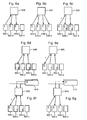
- the peripheral devices shown 600-1 to 600-4 each include a DMA type controller in accordance with the specifications described above. Each of these devices is here connected to a switch 605 adapted to manage collective transfers (multicast and broadcast).
- the figure 6a illustrates a multicast transmission of the device 600-1 to the devices 600-2 and 600-3.
- the data broadcast is thus carried out from a source to several targets of the multicast group to which the device 600-1 belongs. This is a communication type 1 to n initiated by the device comprising the transferred data.
- the figure 6b illustrates a broadcast type transmission from device 600-1 to devices 600-2, 600-3 and 600-4.
- the data broadcast is thus carried out from a source to all the targets of the multicast group to which the device 600-1 belongs. This is a type 1 communication to all initiated by the device comprising the transferred data.
- the Figure 6c illustrates a multicast type transmission calculated from the device 600-1 to the devices 600-2, 600-3 and 600-4.
- the data broadcast is thus carried out from a source to all the targets of the multicast group to which the device 600-1 belongs.
- an operation is performed on the transferred data, for example a logical operation such as "or", "and” or "exclusive", a mathematical operation such as an addition or a multiplication or an operation defined by the device such as a sort of data or their encryption.
- the operation performed here is an addition between the transferred data and a data present in the target device.
- the transmission is initiated by the device comprising the transferred data.
- the figure 6d illustrates a data aggregation type transmission of the devices 600-2 and 600-3 to the device 600-1. It is an operation that allows, from several sources, to transmit data to one or more targets by aggregating the transmitted data. The transmission is initiated by the device receiving the transferred data.
- the figure 6e illustrates a computationally aggregated data transmission of devices 600-2 and 600-3 to the device 600-1. It is an operation that allows, from several sources, to transmit data to a target by performing a calculation on the transmitted data. This is an addition between the data received from the sources used. The transmission is initiated by the device receiving the transferred data. Naturally other types of operations can be implemented.
- the figure 6f illustrates a computationally aggregated data transmission of the devices 600-2 and 600-3 and the central memory 610 to the device 600-1. This is an operation that allows, from several sources, to transmit data to a target by performing a calculation on the transmitted data. This is an addition between the data received from the sources used. The transmission is initiated by the device receiving the transferred data. Other types of operations can also be implemented.
- the figure 6g illustrates a multicast transmission of the device 600-1 to the devices 600-2 and 600-3 and the central memory 610.
- the data broadcast is thus carried out from a source to several targets of the multicast group to which the device belongs 600-1. This is a type 1 to n communication.
- the transmission is initiated by the device comprising the transferred data.
- the choice of the operation to be performed depends on some of the data received in response to a data read command.
- Direct data transfers between several peripheral devices can be implemented using collective transfer primitives determined in at least one of the peripheral devices.
- This implementation is similar to that described above. It includes phases of identification, declaration, configuration and control.
- the parameters of the collective transfer primitives are preferably similar to those of the primitives used to perform a direct transfer of data between memories of two peripheral devices as previously described. However, they also include specific characteristics related in particular to data combining operations.
- the device 600-1 waits to receive the transferred data and then performs the operation specified in the primitive.
- the step 425 described above then comprises a step for initiating the direct memory access control of other devices, a synchronization step for obtaining the expected data and a step for executing the operations specified in the primitive related to the transfer activated.
Landscapes
- Engineering & Computer Science (AREA)
- Theoretical Computer Science (AREA)
- Physics & Mathematics (AREA)
- General Engineering & Computer Science (AREA)
- General Physics & Mathematics (AREA)
- Mathematical Physics (AREA)
- Computer Hardware Design (AREA)
- Bus Control (AREA)
- Multi Processors (AREA)
Claims (10)
- Computersystem mit einer Mehrzahl von peripheren Vorrichtungen (600) und zumindest einem Schalter (605), der mit jeder Vorrichtung aus der Mehrzahl von peripheren Vorrichtungen verbunden ist, wobei der Schalter Mittel zum Übertragen eines Befehls an eine Mehrzahl von Elementen des Computersystems enthält, wobei dieses System dadurch gekennzeichnet ist, dass- zumindest eine Vorrichtung aus der Mehrzahl von peripheren Vorrichtungen, die sogenannte zumindest eine erste periphere Vorrichtung, Mittel zum Initiieren (425) zumindest eines Befehls zum direkten Zugriff auf eine Mehrzahl von Speicherbereichen enthält, wobei jedem der Speicherbereiche ein Element zugeordnet ist, das sich von der Mehrzahl von Elementen unterscheidet;- der Schalter Mittel zum Übertragen zumindest eines Teils des zumindest einen Befehls zum direkten Zugriff an jedes Element der Mehrzahl von Elementen enthält;- zumindest ein Element aus der Mehrzahl von Elementen aus zumindest einer Vorrichtung der Mehrzahl von peripheren Vorrichtungen besteht, die sogenannte zumindest eine zweite periphere Vorrichtung, wobei die zumindest eine zweite periphere Vorrichtung die nachfolgenden Mittel enthält:• Mittel zum Empfangen (400) von zumindest einem Befehl zum direkten Zugriff auf einen Bereich eines Speichers der zweiten peripheren Vorrichtung, wobei der Befehl von der zumindest einen ersten peripheren Vorrichtung über den Schalter empfangen wird; und• Mittel zum Übertragen (415) des zumindest einen empfangenen Befehls zum direkten Zugriff an eine Komponente der zweiten peripheren Vorrichtung,
wobei das System der zumindest einen ersten peripheren Vorrichtung gestattet, eine direkte Übertragung von zumindest einer Datenangabe zu oder von einem Speicher der zumindest einen ersten peripheren Vorrichtung von oder zu jedem Element aus der Mehrzahl von Elementen ausgehend von einem einzigen Befehl durchzuführen. - System nach dem vorangehenden Anspruch, wobei die zumindest eine erste Vorrichtung Mittel zum Durchführen zumindest einer Operation an zumindest einer Datenangabe aus Daten enthält, die von der Mehrzahl von Elementen in Antwort auf den zumindest einen Befehl empfangen wurden.
- System nach dem vorangehenden Anspruch, wobei die zumindest eine Operation zumindest eine Operation aus logischen Operationen, mathematischen Operationen, Sortieroperationen, Codierungsoperationen und Aggregationsoperationen umfasst.
- System nach Anspruch 2 oder Anspruch 3, wobei die Mittel zum Durchführen der zumindest einen Operation Mittel zum Identifizieren der zumindest einen Operation nach zumindest einer Datenangabe aus Daten enthalten, die von der Mehrzahl an Elementen in Antwort auf den zumindest einen Befehl empfangenen wurden.
- System nach einem der vorangehenden Ansprüche, wobei zumindest ein Element aus der Mehrzahl von Elementen einen Zentralspeicher (610) des Computersystems aufweist.
- System nach einem der vorangehenden Ansprüche, wobei zumindest eine zweite periphere Vorrichtung ferner Mittel zum Kontrollieren der Gültigkeit des zumindest einen Teils des zumindest einen Befehls enthält.
- System nach dem vorangehenden Anspruch, wobei die Kontrollmittel Mittel zum Vergleichen einer Identifizierung des Senders des zumindest einen Befehls zum direkten Zugriff mit zumindest einer vorbestimmten Identifizierung enthalten.
- System nach Anspruch 6 oder Anspruch 7, wobei die Kontrollmittel Mittel zum Vergleichen des Bereichs eines Speichers der zweiten peripheren Vorrichtung mit zumindest einem vorbestimmten Speicherbereich enthalten.
- System nach einem der vorangehenden Ansprüche, wobei die Mittel der zumindest einen zweiten Vorrichtung zum Übertragen des zumindest einen empfangenen Befehls zum direkten Zugriff an eine Komponente der zweiten peripheren Vorrichtung Mittel zum Durchführen zumindest einer Operation an zumindest einer empfangen Datenangabe enthalten.
- System nach einem der vorangehenden Ansprüche, wobei die zumindest eine erste periphere Vorrichtung ferner Mittel zum Identifizieren der zumindest einen zweiten peripheren Vorrichtung enthält sowie Mittel zum Übertragen eines Befehls zum direkten Zugriff auf einen Bereich eines Speichers der zweiten Vorrichtung dann, wenn der Speicher, der von dem von den Initiierungsmitteln stammenden Befehl zum direkten Zugriff angepeilt wird, zur zumindest einen zweiten peripheren Vorrichtung gehört.
Applications Claiming Priority (2)
| Application Number | Priority Date | Filing Date | Title |
|---|---|---|---|
| FR0905777A FR2953308B1 (fr) | 2009-12-01 | 2009-12-01 | Systeme autorisant des transferts directs de donnees entre des memoires de plusieurs elements de ce systeme |
| PCT/FR2010/052502 WO2011067507A1 (fr) | 2009-12-01 | 2010-11-24 | Systeme autorisant des transferts directs de donnees entre des memoires de plusieurs elements de ce systeme |
Publications (2)
| Publication Number | Publication Date |
|---|---|
| EP2507712A1 EP2507712A1 (de) | 2012-10-10 |
| EP2507712B1 true EP2507712B1 (de) | 2014-01-22 |
Family
ID=42272350
Family Applications (1)
| Application Number | Title | Priority Date | Filing Date |
|---|---|---|---|
| EP10805264.8A Active EP2507712B1 (de) | 2009-12-01 | 2010-11-24 | System zur direkte datenübertragung zwischen speichern von mehreren elementen dieses systems |
Country Status (6)
| Country | Link |
|---|---|
| US (1) | US9053092B2 (de) |
| EP (1) | EP2507712B1 (de) |
| JP (1) | JP5904948B2 (de) |
| BR (1) | BR112012010409A2 (de) |
| FR (1) | FR2953308B1 (de) |
| WO (1) | WO2011067507A1 (de) |
Families Citing this family (5)
| Publication number | Priority date | Publication date | Assignee | Title |
|---|---|---|---|---|
| GB2497528B (en) | 2011-12-12 | 2020-04-22 | Nordic Semiconductor Asa | Peripheral communication |
| JP6089840B2 (ja) * | 2013-03-21 | 2017-03-08 | 富士通株式会社 | 同期制御装置,同期制御方法および同期制御プログラム |
| US9875202B2 (en) | 2015-03-09 | 2018-01-23 | Nordic Semiconductor Asa | Peripheral communication system with shortcut path |
| GB2540341B (en) | 2015-06-16 | 2019-06-26 | Nordic Semiconductor Asa | Event generating unit |
| GB2539455A (en) | 2015-06-16 | 2016-12-21 | Nordic Semiconductor Asa | Memory watch unit |
Family Cites Families (13)
| Publication number | Priority date | Publication date | Assignee | Title |
|---|---|---|---|---|
| JPH02207363A (ja) * | 1989-02-08 | 1990-08-17 | Hitachi Ltd | データ転送制御方式、デバイスコントローラ、およびメモリ・コントローラ |
| JPH05265923A (ja) * | 1992-03-23 | 1993-10-15 | Mitsubishi Electric Corp | データ転送装置 |
| US20080256352A1 (en) * | 2000-01-06 | 2008-10-16 | Super Talent Electronics, Inc. | Methods and systems of booting of an intelligent non-volatile memory microcontroller from various sources |
| JP3903699B2 (ja) * | 2000-08-10 | 2007-04-11 | 富士通株式会社 | Pciバスによるデータ交換方法及び装置 |
| US6748479B2 (en) * | 2001-11-20 | 2004-06-08 | Broadcom Corporation | System having interfaces and switch that separates coherent and packet traffic |
| JP2005202767A (ja) * | 2004-01-16 | 2005-07-28 | Toshiba Corp | プロセッサシステム、dma制御回路、dma制御方法、dmaコントローラの制御方法、画像処理方法および画像処理回路 |
| JP2005250577A (ja) * | 2004-03-01 | 2005-09-15 | Toshiba Corp | コンピュータシステム及び演算処理モジュールの健全性判定方法 |
| JP2006114822A (ja) * | 2004-10-18 | 2006-04-27 | Fuji Electric Device Technology Co Ltd | 半導体装置の製造方法 |
| KR100958685B1 (ko) | 2005-04-01 | 2010-05-20 | 후지쯔 가부시끼가이샤 | Dma 컨트롤러, 노드, 데이터 전송 제어 방법 및 프로그램을 기록한 컴퓨터 판독가능한 기록 매체 |
| KR100814904B1 (ko) | 2005-12-06 | 2008-03-19 | 한국전자통신연구원 | 칩 내부 회로 간의 데이터 전송을 위한 통신 시스템 |
| JP2007048314A (ja) * | 2006-10-10 | 2007-02-22 | Fujitsu Ltd | データ転送システムにおける送信装置及び受信装置,データ転送システム並びにデータ転送システムのバス制御方法 |
| GB0724439D0 (en) * | 2007-12-14 | 2008-01-30 | Icera Inc | Data transfer |
| JP4516999B2 (ja) * | 2008-03-28 | 2010-08-04 | 富士通株式会社 | データ通信制御装置、データ通信制御方法およびそのためのプログラム |
-
2009
- 2009-12-01 FR FR0905777A patent/FR2953308B1/fr active Active
-
2010
- 2010-11-24 BR BR112012010409A patent/BR112012010409A2/pt active Search and Examination
- 2010-11-24 JP JP2012541556A patent/JP5904948B2/ja active Active
- 2010-11-24 WO PCT/FR2010/052502 patent/WO2011067507A1/fr not_active Ceased
- 2010-11-24 EP EP10805264.8A patent/EP2507712B1/de active Active
- 2010-11-24 US US13/513,040 patent/US9053092B2/en active Active
Also Published As
| Publication number | Publication date |
|---|---|
| FR2953308B1 (fr) | 2011-12-09 |
| BR112012010409A2 (pt) | 2016-02-23 |
| JP2013512520A (ja) | 2013-04-11 |
| FR2953308A1 (fr) | 2011-06-03 |
| US9053092B2 (en) | 2015-06-09 |
| US20120239826A1 (en) | 2012-09-20 |
| WO2011067507A1 (fr) | 2011-06-09 |
| EP2507712A1 (de) | 2012-10-10 |
| JP5904948B2 (ja) | 2016-04-20 |
Similar Documents
| Publication | Publication Date | Title |
|---|---|---|
| EP2507711B1 (de) | Direktspeicherzugriffsteuerung für direkte datenübertragung zwischen mehreren peripheriegerätespeicher | |
| EP2507712B1 (de) | System zur direkte datenübertragung zwischen speichern von mehreren elementen dieses systems | |
| EP2438528A1 (de) | Verfahren und einrichtung zum laden und ausführen von anweisungen mit deterministischen zyklen in einem einen bus aufweisenden mehrkern-avioniksystem, dessen zugriffszeit unvorhersehbar ist | |
| CN103970670A (zh) | 用于使用rdma的数据传输的方法和设备 | |
| CN101005504B (zh) | 网络协议栈隔离方法和系统 | |
| EP3217290A1 (de) | Chipsystem und verfahren zum datenaustausch zwischen rechenknoten eines solchen chipsystems | |
| FR2834361A1 (fr) | Module de securisation de donnees par chiffrement/dechiffrement et/ou signature/verification de signature | |
| EP2751959B1 (de) | Verfahren zum austausch von daten zwischen knoten in einem server-cluster und servercluster zur durchführung des verfahrens | |
| US20250150270A1 (en) | Systems, methods, and apparatuses for securing ownership of objects in a digital ledger | |
| EP1845456A1 (de) | On-Chip System zur Verbindung von externe Funktionsbausteine mit einem einzigen parametrierbaren Kommunikationsprotokoll | |
| CN117389921A (zh) | 一种存储扩展卡和系统 | |
| EP3123330A1 (de) | Elektronisches bauteil mit deterministischer reaktion | |
| FR2815801A1 (fr) | Protocole de transmission d'une pluralite de flux logiques d'echange multiple de couples de commande/reponse sur un canal physique unique d'echange entre maitre et esclave et systeme de suivi et de controle d'execution d'appliquettes | |
| FR2766937A1 (fr) | Protocole et systeme de liaison par bus entre elements d'un microcontroleur | |
| WO2011058260A1 (fr) | Procede et dispositif d'optimisation d'execution d'applications logicielles dans une architecture multiprocesseur comprenant plusieurs controleurs d'entree/sortie et unites de calcul secondaires | |
| US20240235989A1 (en) | Switch port aggregation in centralized software-defined networks (sdn) | |
| FR2919401A1 (fr) | Procede de test des chemins de donnees dans un circuit electronique | |
| EP0466555A1 (de) | Lokales Netzwerk für Interkommunikation zwischen Datenverarbeitungsmodulen | |
| FR2805372A1 (fr) | Postage d'ecriture avec mise en ordre globale dans des systemes a chemins multiples | |
| EP1493083B1 (de) | Umkonfigurierbares steuersystem auf der basis einer hardwareimplementierung von petri-graphen | |
| US20220083492A1 (en) | Multiple field programmable gate array (fpga) based multi-legged order transaction processing system and method thereof | |
| EP2909729B1 (de) | Verfahren und vorrichtung zur verarbeitung von unterbrechungen in einem multiprozessorsystem | |
| FR3154820A1 (fr) | Optimisation des transferts de données entre un processeur de traitement parallèle et une mémoire | |
| WO2018122207A1 (fr) | Dispositif et procede pour creer un environnement de confiance dans un systeme distribue | |
| FR2930697A1 (fr) | Procede et dispositif de configuration dynamique d'un reseau de communication pour la simulation temps reel de l'integration de composants electroniques dans un vehicule |
Legal Events
| Date | Code | Title | Description |
|---|---|---|---|
| PUAI | Public reference made under article 153(3) epc to a published international application that has entered the european phase |
Free format text: ORIGINAL CODE: 0009012 |
|
| 17P | Request for examination filed |
Effective date: 20120326 |
|
| AK | Designated contracting states |
Kind code of ref document: A1 Designated state(s): AL AT BE BG CH CY CZ DE DK EE ES FI FR GB GR HR HU IE IS IT LI LT LU LV MC MK MT NL NO PL PT RO RS SE SI SK SM TR |
|
| DAX | Request for extension of the european patent (deleted) | ||
| GRAP | Despatch of communication of intention to grant a patent |
Free format text: ORIGINAL CODE: EPIDOSNIGR1 |
|
| INTG | Intention to grant announced |
Effective date: 20130903 |
|
| GRAS | Grant fee paid |
Free format text: ORIGINAL CODE: EPIDOSNIGR3 |
|
| GRAA | (expected) grant |
Free format text: ORIGINAL CODE: 0009210 |
|
| AK | Designated contracting states |
Kind code of ref document: B1 Designated state(s): AL AT BE BG CH CY CZ DE DK EE ES FI FR GB GR HR HU IE IS IT LI LT LU LV MC MK MT NL NO PL PT RO RS SE SI SK SM TR |
|
| REG | Reference to a national code |
Ref country code: GB Ref legal event code: FG4D Free format text: NOT ENGLISH |
|
| REG | Reference to a national code |
Ref country code: CH Ref legal event code: EP |
|
| REG | Reference to a national code |
Ref country code: AT Ref legal event code: REF Ref document number: 651080 Country of ref document: AT Kind code of ref document: T Effective date: 20140215 |
|
| REG | Reference to a national code |
Ref country code: IE Ref legal event code: FG4D Free format text: LANGUAGE OF EP DOCUMENT: FRENCH |
|
| REG | Reference to a national code |
Ref country code: DE Ref legal event code: R096 Ref document number: 602010013371 Country of ref document: DE Effective date: 20140306 |
|
| REG | Reference to a national code |
Ref country code: NL Ref legal event code: VDEP Effective date: 20140122 |
|
| REG | Reference to a national code |
Ref country code: AT Ref legal event code: MK05 Ref document number: 651080 Country of ref document: AT Kind code of ref document: T Effective date: 20140122 |
|
| REG | Reference to a national code |
Ref country code: LT Ref legal event code: MG4D |
|
| PG25 | Lapsed in a contracting state [announced via postgrant information from national office to epo] |
Ref country code: IS Free format text: LAPSE BECAUSE OF FAILURE TO SUBMIT A TRANSLATION OF THE DESCRIPTION OR TO PAY THE FEE WITHIN THE PRESCRIBED TIME-LIMIT Effective date: 20140522 Ref country code: NO Free format text: LAPSE BECAUSE OF FAILURE TO SUBMIT A TRANSLATION OF THE DESCRIPTION OR TO PAY THE FEE WITHIN THE PRESCRIBED TIME-LIMIT Effective date: 20140422 Ref country code: LT Free format text: LAPSE BECAUSE OF FAILURE TO SUBMIT A TRANSLATION OF THE DESCRIPTION OR TO PAY THE FEE WITHIN THE PRESCRIBED TIME-LIMIT Effective date: 20140122 |
|
| PG25 | Lapsed in a contracting state [announced via postgrant information from national office to epo] |
Ref country code: NL Free format text: LAPSE BECAUSE OF FAILURE TO SUBMIT A TRANSLATION OF THE DESCRIPTION OR TO PAY THE FEE WITHIN THE PRESCRIBED TIME-LIMIT Effective date: 20140122 Ref country code: CY Free format text: LAPSE BECAUSE OF FAILURE TO SUBMIT A TRANSLATION OF THE DESCRIPTION OR TO PAY THE FEE WITHIN THE PRESCRIBED TIME-LIMIT Effective date: 20140122 Ref country code: FI Free format text: LAPSE BECAUSE OF FAILURE TO SUBMIT A TRANSLATION OF THE DESCRIPTION OR TO PAY THE FEE WITHIN THE PRESCRIBED TIME-LIMIT Effective date: 20140122 Ref country code: SE Free format text: LAPSE BECAUSE OF FAILURE TO SUBMIT A TRANSLATION OF THE DESCRIPTION OR TO PAY THE FEE WITHIN THE PRESCRIBED TIME-LIMIT Effective date: 20140122 Ref country code: ES Free format text: LAPSE BECAUSE OF FAILURE TO SUBMIT A TRANSLATION OF THE DESCRIPTION OR TO PAY THE FEE WITHIN THE PRESCRIBED TIME-LIMIT Effective date: 20140122 Ref country code: PT Free format text: LAPSE BECAUSE OF FAILURE TO SUBMIT A TRANSLATION OF THE DESCRIPTION OR TO PAY THE FEE WITHIN THE PRESCRIBED TIME-LIMIT Effective date: 20140522 Ref country code: AT Free format text: LAPSE BECAUSE OF FAILURE TO SUBMIT A TRANSLATION OF THE DESCRIPTION OR TO PAY THE FEE WITHIN THE PRESCRIBED TIME-LIMIT Effective date: 20140122 |
|
| PG25 | Lapsed in a contracting state [announced via postgrant information from national office to epo] |
Ref country code: RS Free format text: LAPSE BECAUSE OF FAILURE TO SUBMIT A TRANSLATION OF THE DESCRIPTION OR TO PAY THE FEE WITHIN THE PRESCRIBED TIME-LIMIT Effective date: 20140122 Ref country code: HR Free format text: LAPSE BECAUSE OF FAILURE TO SUBMIT A TRANSLATION OF THE DESCRIPTION OR TO PAY THE FEE WITHIN THE PRESCRIBED TIME-LIMIT Effective date: 20140122 Ref country code: LV Free format text: LAPSE BECAUSE OF FAILURE TO SUBMIT A TRANSLATION OF THE DESCRIPTION OR TO PAY THE FEE WITHIN THE PRESCRIBED TIME-LIMIT Effective date: 20140122 |
|
| REG | Reference to a national code |
Ref country code: DE Ref legal event code: R097 Ref document number: 602010013371 Country of ref document: DE |
|
| PG25 | Lapsed in a contracting state [announced via postgrant information from national office to epo] |
Ref country code: DK Free format text: LAPSE BECAUSE OF FAILURE TO SUBMIT A TRANSLATION OF THE DESCRIPTION OR TO PAY THE FEE WITHIN THE PRESCRIBED TIME-LIMIT Effective date: 20140122 Ref country code: EE Free format text: LAPSE BECAUSE OF FAILURE TO SUBMIT A TRANSLATION OF THE DESCRIPTION OR TO PAY THE FEE WITHIN THE PRESCRIBED TIME-LIMIT Effective date: 20140122 Ref country code: RO Free format text: LAPSE BECAUSE OF FAILURE TO SUBMIT A TRANSLATION OF THE DESCRIPTION OR TO PAY THE FEE WITHIN THE PRESCRIBED TIME-LIMIT Effective date: 20140122 Ref country code: CZ Free format text: LAPSE BECAUSE OF FAILURE TO SUBMIT A TRANSLATION OF THE DESCRIPTION OR TO PAY THE FEE WITHIN THE PRESCRIBED TIME-LIMIT Effective date: 20140122 |
|
| PG25 | Lapsed in a contracting state [announced via postgrant information from national office to epo] |
Ref country code: SK Free format text: LAPSE BECAUSE OF FAILURE TO SUBMIT A TRANSLATION OF THE DESCRIPTION OR TO PAY THE FEE WITHIN THE PRESCRIBED TIME-LIMIT Effective date: 20140122 Ref country code: PL Free format text: LAPSE BECAUSE OF FAILURE TO SUBMIT A TRANSLATION OF THE DESCRIPTION OR TO PAY THE FEE WITHIN THE PRESCRIBED TIME-LIMIT Effective date: 20140122 |
|
| PLBE | No opposition filed within time limit |
Free format text: ORIGINAL CODE: 0009261 |
|
| STAA | Information on the status of an ep patent application or granted ep patent |
Free format text: STATUS: NO OPPOSITION FILED WITHIN TIME LIMIT |
|
| 26N | No opposition filed |
Effective date: 20141023 |
|
| REG | Reference to a national code |
Ref country code: DE Ref legal event code: R097 Ref document number: 602010013371 Country of ref document: DE Effective date: 20141023 |
|
| PG25 | Lapsed in a contracting state [announced via postgrant information from national office to epo] |
Ref country code: SI Free format text: LAPSE BECAUSE OF FAILURE TO SUBMIT A TRANSLATION OF THE DESCRIPTION OR TO PAY THE FEE WITHIN THE PRESCRIBED TIME-LIMIT Effective date: 20140122 |
|
| PG25 | Lapsed in a contracting state [announced via postgrant information from national office to epo] |
Ref country code: BE Free format text: LAPSE BECAUSE OF NON-PAYMENT OF DUE FEES Effective date: 20141130 Ref country code: LU Free format text: LAPSE BECAUSE OF FAILURE TO SUBMIT A TRANSLATION OF THE DESCRIPTION OR TO PAY THE FEE WITHIN THE PRESCRIBED TIME-LIMIT Effective date: 20141124 Ref country code: MC Free format text: LAPSE BECAUSE OF FAILURE TO SUBMIT A TRANSLATION OF THE DESCRIPTION OR TO PAY THE FEE WITHIN THE PRESCRIBED TIME-LIMIT Effective date: 20140122 |
|
| REG | Reference to a national code |
Ref country code: CH Ref legal event code: PL |
|
| PG25 | Lapsed in a contracting state [announced via postgrant information from national office to epo] |
Ref country code: LI Free format text: LAPSE BECAUSE OF NON-PAYMENT OF DUE FEES Effective date: 20141130 Ref country code: CH Free format text: LAPSE BECAUSE OF NON-PAYMENT OF DUE FEES Effective date: 20141130 |
|
| REG | Reference to a national code |
Ref country code: IE Ref legal event code: MM4A |
|
| REG | Reference to a national code |
Ref country code: FR Ref legal event code: PLFP Year of fee payment: 6 |
|
| PG25 | Lapsed in a contracting state [announced via postgrant information from national office to epo] |
Ref country code: IE Free format text: LAPSE BECAUSE OF NON-PAYMENT OF DUE FEES Effective date: 20141124 |
|
| PG25 | Lapsed in a contracting state [announced via postgrant information from national office to epo] |
Ref country code: SM Free format text: LAPSE BECAUSE OF FAILURE TO SUBMIT A TRANSLATION OF THE DESCRIPTION OR TO PAY THE FEE WITHIN THE PRESCRIBED TIME-LIMIT Effective date: 20140122 |
|
| PG25 | Lapsed in a contracting state [announced via postgrant information from national office to epo] |
Ref country code: GR Free format text: LAPSE BECAUSE OF FAILURE TO SUBMIT A TRANSLATION OF THE DESCRIPTION OR TO PAY THE FEE WITHIN THE PRESCRIBED TIME-LIMIT Effective date: 20140423 Ref country code: BG Free format text: LAPSE BECAUSE OF FAILURE TO SUBMIT A TRANSLATION OF THE DESCRIPTION OR TO PAY THE FEE WITHIN THE PRESCRIBED TIME-LIMIT Effective date: 20140122 |
|
| PG25 | Lapsed in a contracting state [announced via postgrant information from national office to epo] |
Ref country code: HU Free format text: LAPSE BECAUSE OF FAILURE TO SUBMIT A TRANSLATION OF THE DESCRIPTION OR TO PAY THE FEE WITHIN THE PRESCRIBED TIME-LIMIT; INVALID AB INITIO Effective date: 20101124 Ref country code: TR Free format text: LAPSE BECAUSE OF FAILURE TO SUBMIT A TRANSLATION OF THE DESCRIPTION OR TO PAY THE FEE WITHIN THE PRESCRIBED TIME-LIMIT Effective date: 20140122 Ref country code: MT Free format text: LAPSE BECAUSE OF FAILURE TO SUBMIT A TRANSLATION OF THE DESCRIPTION OR TO PAY THE FEE WITHIN THE PRESCRIBED TIME-LIMIT Effective date: 20140122 |
|
| REG | Reference to a national code |
Ref country code: FR Ref legal event code: PLFP Year of fee payment: 7 |
|
| REG | Reference to a national code |
Ref country code: FR Ref legal event code: PLFP Year of fee payment: 8 |
|
| PG25 | Lapsed in a contracting state [announced via postgrant information from national office to epo] |
Ref country code: MK Free format text: LAPSE BECAUSE OF FAILURE TO SUBMIT A TRANSLATION OF THE DESCRIPTION OR TO PAY THE FEE WITHIN THE PRESCRIBED TIME-LIMIT Effective date: 20140122 |
|
| PG25 | Lapsed in a contracting state [announced via postgrant information from national office to epo] |
Ref country code: AL Free format text: LAPSE BECAUSE OF FAILURE TO SUBMIT A TRANSLATION OF THE DESCRIPTION OR TO PAY THE FEE WITHIN THE PRESCRIBED TIME-LIMIT Effective date: 20140122 |
|
| PGFP | Annual fee paid to national office [announced via postgrant information from national office to epo] |
Ref country code: IT Payment date: 20191122 Year of fee payment: 10 |
|
| PG25 | Lapsed in a contracting state [announced via postgrant information from national office to epo] |
Ref country code: IT Free format text: LAPSE BECAUSE OF NON-PAYMENT OF DUE FEES Effective date: 20201124 |
|
| REG | Reference to a national code |
Ref country code: GB Ref legal event code: 732E Free format text: REGISTERED BETWEEN 20230105 AND 20230111 |
|
| REG | Reference to a national code |
Ref country code: DE Ref legal event code: R081 Ref document number: 602010013371 Country of ref document: DE Owner name: COMMISSARIAT A L'ENERGIE ATOMIQUE ET AUX ENERG, FR Free format text: FORMER OWNER: BULL SAS, LES CLAYES-SOUS-BOIS, FR Ref country code: DE Ref legal event code: R081 Ref document number: 602010013371 Country of ref document: DE Owner name: BULL SAS, FR Free format text: FORMER OWNER: BULL SAS, LES CLAYES-SOUS-BOIS, FR Ref country code: DE Ref legal event code: R082 Ref document number: 602010013371 Country of ref document: DE Representative=s name: BRANDSTOCK LEGAL RECHTSANWALTSGESELLSCHAFT MBH, DE |
|
| P01 | Opt-out of the competence of the unified patent court (upc) registered |
Effective date: 20230330 |
|
| PGFP | Annual fee paid to national office [announced via postgrant information from national office to epo] |
Ref country code: DE Payment date: 20251118 Year of fee payment: 16 |
|
| PGFP | Annual fee paid to national office [announced via postgrant information from national office to epo] |
Ref country code: GB Payment date: 20251120 Year of fee payment: 16 |
|
| PGFP | Annual fee paid to national office [announced via postgrant information from national office to epo] |
Ref country code: FR Payment date: 20251120 Year of fee payment: 16 |