EP2508947A1 - Composition de résine photosensible, stratifié l'utilisant et dispositif d'imagerie à l'état solide - Google Patents
Composition de résine photosensible, stratifié l'utilisant et dispositif d'imagerie à l'état solide Download PDFInfo
- Publication number
- EP2508947A1 EP2508947A1 EP10834451A EP10834451A EP2508947A1 EP 2508947 A1 EP2508947 A1 EP 2508947A1 EP 10834451 A EP10834451 A EP 10834451A EP 10834451 A EP10834451 A EP 10834451A EP 2508947 A1 EP2508947 A1 EP 2508947A1
- Authority
- EP
- European Patent Office
- Prior art keywords
- photosensitive resin
- light
- wavelength
- resin composition
- permeability
- Prior art date
- Legal status (The legal status is an assumption and is not a legal conclusion. Google has not performed a legal analysis and makes no representation as to the accuracy of the status listed.)
- Withdrawn
Links
Images

Classifications
-
- G—PHYSICS
- G03—PHOTOGRAPHY; CINEMATOGRAPHY; ANALOGOUS TECHNIQUES USING WAVES OTHER THAN OPTICAL WAVES; ELECTROGRAPHY; HOLOGRAPHY
- G03F—PHOTOMECHANICAL PRODUCTION OF TEXTURED OR PATTERNED SURFACES, e.g. FOR PRINTING, FOR PROCESSING OF SEMICONDUCTOR DEVICES; MATERIALS THEREFOR; ORIGINALS THEREFOR; APPARATUS SPECIALLY ADAPTED THEREFOR
- G03F7/00—Photomechanical, e.g. photolithographic, production of textured or patterned surfaces, e.g. printing surfaces; Materials therefor, e.g. comprising photoresists; Apparatus specially adapted therefor
- G03F7/004—Photosensitive materials
- G03F7/027—Non-macromolecular photopolymerisable compounds having carbon-to-carbon double bonds, e.g. ethylenic compounds
- G03F7/028—Non-macromolecular photopolymerisable compounds having carbon-to-carbon double bonds, e.g. ethylenic compounds with photosensitivity-increasing substances, e.g. photoinitiators
- G03F7/031—Organic compounds not covered by group G03F7/029
-
- G—PHYSICS
- G03—PHOTOGRAPHY; CINEMATOGRAPHY; ANALOGOUS TECHNIQUES USING WAVES OTHER THAN OPTICAL WAVES; ELECTROGRAPHY; HOLOGRAPHY
- G03F—PHOTOMECHANICAL PRODUCTION OF TEXTURED OR PATTERNED SURFACES, e.g. FOR PRINTING, FOR PROCESSING OF SEMICONDUCTOR DEVICES; MATERIALS THEREFOR; ORIGINALS THEREFOR; APPARATUS SPECIALLY ADAPTED THEREFOR
- G03F7/00—Photomechanical, e.g. photolithographic, production of textured or patterned surfaces, e.g. printing surfaces; Materials therefor, e.g. comprising photoresists; Apparatus specially adapted therefor
- G03F7/004—Photosensitive materials
- G03F7/0042—Photosensitive materials with inorganic or organometallic light-sensitive compounds not otherwise provided for, e.g. inorganic resists
-
- G—PHYSICS
- G03—PHOTOGRAPHY; CINEMATOGRAPHY; ANALOGOUS TECHNIQUES USING WAVES OTHER THAN OPTICAL WAVES; ELECTROGRAPHY; HOLOGRAPHY
- G03F—PHOTOMECHANICAL PRODUCTION OF TEXTURED OR PATTERNED SURFACES, e.g. FOR PRINTING, FOR PROCESSING OF SEMICONDUCTOR DEVICES; MATERIALS THEREFOR; ORIGINALS THEREFOR; APPARATUS SPECIALLY ADAPTED THEREFOR
- G03F7/00—Photomechanical, e.g. photolithographic, production of textured or patterned surfaces, e.g. printing surfaces; Materials therefor, e.g. comprising photoresists; Apparatus specially adapted therefor
- G03F7/004—Photosensitive materials
- G03F7/0045—Photosensitive materials with organic non-macromolecular light-sensitive compounds not otherwise provided for, e.g. dissolution inhibitors
-
- G—PHYSICS
- G03—PHOTOGRAPHY; CINEMATOGRAPHY; ANALOGOUS TECHNIQUES USING WAVES OTHER THAN OPTICAL WAVES; ELECTROGRAPHY; HOLOGRAPHY
- G03F—PHOTOMECHANICAL PRODUCTION OF TEXTURED OR PATTERNED SURFACES, e.g. FOR PRINTING, FOR PROCESSING OF SEMICONDUCTOR DEVICES; MATERIALS THEREFOR; ORIGINALS THEREFOR; APPARATUS SPECIALLY ADAPTED THEREFOR
- G03F7/00—Photomechanical, e.g. photolithographic, production of textured or patterned surfaces, e.g. printing surfaces; Materials therefor, e.g. comprising photoresists; Apparatus specially adapted therefor
- G03F7/004—Photosensitive materials
- G03F7/027—Non-macromolecular photopolymerisable compounds having carbon-to-carbon double bonds, e.g. ethylenic compounds
- G03F7/032—Non-macromolecular photopolymerisable compounds having carbon-to-carbon double bonds, e.g. ethylenic compounds with binders
- G03F7/037—Non-macromolecular photopolymerisable compounds having carbon-to-carbon double bonds, e.g. ethylenic compounds with binders the binders being polyamides or polyimides
-
- G—PHYSICS
- G03—PHOTOGRAPHY; CINEMATOGRAPHY; ANALOGOUS TECHNIQUES USING WAVES OTHER THAN OPTICAL WAVES; ELECTROGRAPHY; HOLOGRAPHY
- G03F—PHOTOMECHANICAL PRODUCTION OF TEXTURED OR PATTERNED SURFACES, e.g. FOR PRINTING, FOR PROCESSING OF SEMICONDUCTOR DEVICES; MATERIALS THEREFOR; ORIGINALS THEREFOR; APPARATUS SPECIALLY ADAPTED THEREFOR
- G03F7/00—Photomechanical, e.g. photolithographic, production of textured or patterned surfaces, e.g. printing surfaces; Materials therefor, e.g. comprising photoresists; Apparatus specially adapted therefor
- G03F7/004—Photosensitive materials
- G03F7/09—Photosensitive materials characterised by structural details, e.g. supports, auxiliary layers
- G03F7/091—Photosensitive materials characterised by structural details, e.g. supports, auxiliary layers characterised by antireflection means or light filtering or absorbing means, e.g. anti-halation, contrast enhancement
-
- H—ELECTRICITY
- H10—SEMICONDUCTOR DEVICES; ELECTRIC SOLID-STATE DEVICES NOT OTHERWISE PROVIDED FOR
- H10F—INORGANIC SEMICONDUCTOR DEVICES SENSITIVE TO INFRARED RADIATION, LIGHT, ELECTROMAGNETIC RADIATION OF SHORTER WAVELENGTH OR CORPUSCULAR RADIATION
- H10F99/00—Subject matter not provided for in other groups of this subclass
Definitions
- the present invention relates to a photosensitive resin composition, a laminate utilizing the same and a solid-state imaging device.
- CMOS complementary metal-oxide semiconductors
- a small-sized solid-state imaging device comprising a solid-state imaging element, a passive chip that is bonded to the back surface of the solid-state imaging element and electrically connected to the solid-state imaging element, has a terminal for electrical connection to outside on a surface opposite to the surface bonded to the solid-state imaging element, and is provided with a passive component, a dam-like spacer, and a lens holder (see, for example, Patent Document 1) and a camera module comprising a semiconductor substrate with a solid-state imaging element formed thereon, a bonding pad, multiple through electrodes and side electrodes, a passive component electrically connected among the side electrodes and placed on the side surface of the semiconductor substrate, a microlens, a spacer resin, an optical filter and a lens
- FIG. 1 One example of the configuration of a solid-state imaging device is shown in Figure 1 .
- the solid-state imaging device has a lens holder 9 on a semiconductor substrate 3 with a solid-state imaging element 2 formed thereon, and a lens 10 and a glass 11 are caught by the lens holder 9.
- the glass 11 is formed on the solid-state imaging element 2, and an IR cut filter 8 caught by the lens holder 9 is mounted via a spacer 12.
- a solder ball 1 is formed at the tip of a through electrode 7 extending through the semiconductor substrate 3 with the solid-state imaging element 2 formed thereon, and the semiconductor substrate 3 and a mounting substrate 4 for mounting the same are connected by the solder ball 1.
- the semiconductor substrate 3 has an insulating layer 5 on the surface at the mounting substrate 4 side.
- a silicon wafer that is commonly used as the semiconductor substrate 3 shields against light having a wavelength in an ultraviolet range and a visible range, but is permeable to light having a wavelength in a near-infrared range, and therefore incidence of light having a wavelength in an ultraviolet range, a visible range and a near-infrared range is prevented by providing a light-shielding layer 6 that shields against light having a wavelength in a near-infrared range.
- a negative photosensitive resin composition containing an alkali-soluble resin, a compound having at least two polymerizable groups, a photoacid generator, a crosslinker that is reacted by an acid and (E) a solvent (see, for example, Patent Document 3).
- a dispersion of a near-infrared absorber in which a near-infrared absorber constituted by hexaboride particles having an average particle size of 200 nm or less and comprising at least one element selected from Y, La, Ce, Pr, Nd, Sm, Eu, Gd, Tb, Dy, Ho, Er, Tm, Yb, Lu, Sr and Ca is dispersed in a liquid medium (see, for example, Patent Document 4) and a vinyl chloride-based resin composition containing 0.01 to 10 parts by mass of at least one infrared absorber selected from (a) a metal ion including a bivalent copper ion and (b) a particulate metal oxide including indium oxide and/or tin oxide and 10 to 200 parts by mass of plasticizer based on 100 parts by mass of vinyl chloride-based resin (see, for example, Patent Document 4)
- a vinyl chloride-based resin composition containing 0.01 to 10 parts by mass of at least one infrared absorb
- a near-infrared absorber filter for a plasma display panel which contains tungsten oxide particulates and/or composite tungsten oxide particulates having an average dispersion particle size of 800 nm or less and has such properties that the maximum value of the permeability to visible light having a wavelength of 380 to 780 nm is 50% or more and the minimum value of the permeability to near-infrared light having a wavelength of 800 to 1100 nm is 30% or less (see, for example, Patent Document 6).
- a solid-state imaging device having a configuration shown in Figure 1 has a problem in productivity because multiple materials are applied such that an insulating material is applied onto the back surface of a semiconductor substrate, followed by applying a material shielding against light having a wavelength in a near-infrared range to thereby deposit an insulating layer and a light-shielding layer.
- an object of the present invention is to provide a photosensitive resin composition which can more simply impart insulating properties and light-shielding properties against light having a wavelength lying in an ultraviolet range, a visible range and a near-infrared range when applied onto a substrate which has such properties that the permeability to light having a wavelength of 400 to 900 nm inclusive is less than 3.0% and the maximum value of the permeability to light having a wavelength longer than 900 nm and no longer than 1300 nm is 3.0% or more.
- the present invention is a photosensitive resin composition which contains (a) an alkali-soluble resin, (b) a tungsten oxide and/or a composite tungsten oxide represented by the following general formula (1) or (2), (c) a photopolymerizable compound having at least two polymerizable groups, (d) an oxime-type photopolymerization initiator, and (e) a solvent.
- W is tungsten, O is oxygen, y > 0, z > 0, and the requirement of 2.2 ⁇ z/y ⁇ 3 is met.
- element M is at least one element selected from H, He, an alkali metal, an alkali earth metal, a rare earth element, Mg, Zr, Cr, Mn, Fe, Ru, Co, Rh, Ir, Ni, Pd, Pt, Cu, Ag, Au, Zn, Cd, Al, Ga, In, Tl, Si, Ge, Sn, Pb, Sb, B, F, P, S, Se, Br, Te, Ti, Nb, V, Mo, Ta, Re, Be, Hf, Os, Bi and I, W is tungsten, O is oxygen, x > 0, y > 0, z > 0 and the requirements of 0.001 ⁇ x/y ⁇ 1.1 and 2.2 ⁇ z/y
- Insulating properties and light-shielding properties against light having a wavelength lying in an ultraviolet range, a visible range and a near-infrared range can be imparted by applying a photosensitive resin composition of the present invention onto a substrate which has such properties that the permeability to light having a wavelength of 400 to 900 nm inclusive is less than 3.0% and the maximum value of the permeability to light having a wavelength longer than 900 nm and no longer than 1300 nm is 3.0% or more. Accordingly, a solid-state imaging device can be provided using a simpler and more productive method.
- a photosensitive resin composition of the present invention contains (a) an alkali-soluble resin.
- Alkali solubility in the present invention means that a dissolution rate is 50 nm/minute or more, the dissolution rate being determined from a decrease in film thickness when a solution of a resin in ⁇ -butyrolactone is applied onto a silicon wafer and prebaked at 120°C for 4 minutes to form a prebake film having a thickness of 10 ⁇ m ⁇ 0.5 ⁇ m, and the prebake film is immersed in a 2.38 wt% aqueous tetramethyl ammonium hydroxide solution at 23 ⁇ 1°C for one minute and then rinsed with pure water.
- the alkali-soluble resin to be used in the present invention preferably has an acidic group in a structure unit of a resin and/or at the end of the backbone thereof because the group imparts the alkali solubility described above.
- the acidic group include a carboxyl group, a phenolic hydroxyl group, a sulfonic acid group and a thiol group.
- the resin preferably has fluorine atoms, by which water-repellency can be imparted to a film boundary to suppress penetration through the boundary.
- the content of fluorine atoms in the alkali-soluble resin is preferably 5% by weight or more from the viewpoint of prevention of penetration through the boundary, and preferably 20% by weight or less from the viewpoint of solubility in an aqueous alkali solution.
- the photosensitive resin composition of the present invention preferably uses as (a) the alkali-soluble resin, (a) a polyimide, a polybenzoxazole or a precursor thereof.
- the polyimide and polybenzoxazole are resins having a cyclic structure of an imide ring or an oxazole ring within a backbone structure.
- the polyimide precursor and polybenzoxazole precursor are resins having an amide bond in the backbone, and are converted into the polyimide or polybenzoxazole through dewatering cyclization by a heating treatment or a chemical treatment. By incorporating these resins, a resin composition excellent in insulating properties can be obtained.
- polyimide precursor may include polyamide acids, polyamide acid esters, polyamide acid amides and polyisoimides.
- examples of the polybenzoxazole precursor may include polyhydroxyamides, polyaminoamides, polyamides and polyamideimides. In any case, the number of repetitions of structural units is preferably 10 to 100000. Two or more kinds thereof may be contained or a copolymer having such two or more kinds of structural units may be contained.
- a polyimide is more preferable from the viewpoint of chemical resistance when cured by a heat treatment at a low temperature of 250°C or lower.
- the polyimide is generally obtained by dewatering-cyclizing a polyamide acid, which is one polyimide precursor obtained by reacting a tetracarboxylic dianhydride with a diamine, by heating or a chemical treatment with an acid or a base, and has a tetracarboxylic acid residue and a diamine residue.
- a polyamide acid which is one polyimide precursor obtained by reacting a tetracarboxylic dianhydride with a diamine, by heating or a chemical treatment with an acid or a base, and has a tetracarboxylic acid residue and a diamine residue.
- the polyimide is preferably one having a structural unit represented by the following general formula (3). It may contain two or more kinds thereof or may be a copolymer with other structural unit.
- the structural unit represented by the following general formula (3) or general formula (4) described later is preferably contained in an amount of 50 mol% or more among all structural units.
- R 1 represents a tetra-to decavalent organic group and R 2 represents a bi- to octavalent organic group.
- R 3 and R 4 represent a phenolic hydroxyl group, a sulfonic acid group or a thiol group, and may each be same or different.
- p and q represent an integer of 0 to 6, and may each be same or different.
- R 1 -(R 3 ) p represents a tetracarboxylic acid residue.
- R 1 is a tetra- to decavalent organic group, and is preferably a tetra- to decavalent organic group having 5 to 40 carbon atoms, which has an aromatic ring or a cyclic aliphatic group.
- an acid dianhydride constituting the tetracarboxylic residue examples include aromatic tetracarboxylic dianhydrides such as pyromellitic dianhydride, 3,3',4,4'-biphenyltetracarboxylic dianhydride, 2,3,3',4'-biphenyltetracarboxylic dianhydride, 2,2',3,3'-biphenyltetracarboxylic dianhydride, 3,3',4,4'-benzophenonetetracarboxylic dianhydride, 2,2',3,3'-benzophenonetetracarboxylic dianhydride, 2,2-bis(3,4-dicarboxyphenyl)propane dianhydride, 2,2-bis(2,3-dicarboxyphenyl)propane dianhydride, 1,1-bis(3,4-dicarboxyphenyl)ethane dianhydride, 1,1-bis(2,3-dicarboxyphenyl
- R 10 represents an oxygen atom, C(CF 3 ) 2 , C(CH 3 ) 2 or SO 2 .
- R 11 and R 12 represent a hydrogen atom, a hydroxyl group or a thiol group.
- R 2 -(R 4 ) q represents a diamine residue.
- R 2 is a bi- to octavalent organic group, and is preferably a bi- to octavalent organic group having 5 to 40 carbon atoms, which has an aromatic ring or a cyclic aliphatic group.
- Examples of a diamine constituting the diamine residue include 3,4'-diaminodiphenyl ether, 4,4'-diaminodiphenyl ether, 3,4'-diaminodiphenyl methane, 4,4'-diaminodiphenylmethane, 3,4'-diaminodiphenylsulfone, 4,4'-diaminodiphenyl sulfone, 3,4'-diaminodiphenyl sulfide, 4,4'-diaminodiphenyl sulfide, 1,4-bis(4-aminophenoxy)benzene, benzine, m-phenylene diamine, p-phenylene diamine, 1,5-naphthalene diamine, 2,6-naphthalene diamine, bis(4-aminophenoxyphenyl)sulfone, bis(3-aminophenoxyphenyl)sulfone, bis(4-
- R 10 represents an oxygen atom, C(CF 3 ) 2 , C(CH 3 ) 2 or SO 2 .
- R 11 to R 14 represent a hydrogen atom, a hydroxyl group or a thiol group.
- the polybenzoxazole can be obtained by reacting a bisaminophenol with a dicarboxylic acid, a corresponding dicarboxylic acid chloride, a dicarboxylic acid active ester or the like. Generally, it can be obtained by dewatering-cyclizing a polyhydroxyamide, which is one polybenzoxazole precursor obtained by reacting a bisaminophenol compound with a dicarboxylic acid, by heating or a chemical treatment with a phosphoric anhydride, a base, a carbodiimide compound or the like, and has a dicarboxylic acid residue and a bisaminophenol residue.
- Examples of an acid constituting the dicarboxylic acid residue include terephthalic acid, isophthalic acid, diphenyletherdicarboxylic acid, bis(carboxyphenyl)hexafluoropropane, biphenyldicarboxylic acid, benzophenonedicarboxylic acid and triphenyldicarboxylic acid. Two or more kinds thereof may be used.
- Examples of a diamine constituting the bisaminophenol residue include diamines having the structure shown below. Two or more kinds thereof may be used.
- R 10 represents an oxygen atom, C(CF 3 ) 2 , C(CH 3 ) 2 or SO 2 .
- R 11 to R 14 represent a hydrogen atom, a hydroxyl group or a thiol group, and at least one in each diamine is a hydroxyl group.
- the polyimide precursor is obtained by, for example, reacting a tetracarboxylic dianhydride (part of which may be substituted by an acid anhydride, a monoacid chloride compound or a mono-active ester compound) with a diamine compound, and has a tetracarboxylic acid residue and a diamine residue.
- a tetracarboxylic dianhydride part of which may be substituted by an acid anhydride, a monoacid chloride compound or a mono-active ester compound
- the polybenzoxazole precursor is obtained by, for example, reacting a bisaminophenol compound with a dicarboxylic acid, and has a dicarboxylic acid residue and a bisaminophenol residue.
- the polyimide precursor and the polybenzoxazole precursor preferably have the general formula (4) described below. They may contain two or more kinds thereof or may be a copolymer with other structural unit.
- the structural unit represented by the following general formula (4) or the above general formula (3) is preferably contained in an amount of 50 mol% or more among all structural units.
- R 5 and R 6 represent a bi- to octavalent organic group and each may be same or different.
- R 7 and R 8 represent a phenolic hydroxyl group, a sulfonic acid group, a thiol group or COOR 9 and may each be same or different.
- R 9 represents a hydrogen atom or a monovalent hydrocarbon group having 1 to 20 carbon atoms. r and s represent an integer of 0 to 6, where r + s > 0.
- R 5 -(R 7 ) r represents a acid residue of a dicarboxylic acid, a tetracarboxylic acid, or the like.
- R 5 is a bi- to octavalent organic group, and is preferably a bi- to octavalent organic group having 5 to 40 carbon atoms, which contains an aromatic ring or a cyclic aliphatic group.
- an acid constituting the acid residue for example, those exemplified as the acid constituting the dicarboxylic acid residue of polybenzoxazole may be mentioned as examples of a dicarboxylic acid.
- a tricarboxylic acid trimellitic acid, trimesic acid, dipehnylethertricarboxylic acid, and biphenyltricarboxylic acid may be mentioned.
- aromatic tetracarboxylic acids such as 3,3',4,4'-biphenyltetracarboxylic acid, 2,3,3',4'-biphenyltetracarboxylic acid, 2,2',3,3'-biphenyltetracarboxylic acid, 3,3',4,4'-benzophenonetetracarboxylic acid, 2,2',3,3'-benzophenonetetracarboxylic acid, 2,2-bis(3,4-dicarboxylphenyl)hexafluoropropane, 2,2-bis(2,3-dicarboxyphenyl)hexafluoropropane, 1,1-bis(3,4-dicarboxyphenyl)ethane, 1,1-bis(2,3-dicarboxyphenyl)ethane, bis(3,4-dicarboxyphenyl)methane, bis(2,3-dicar
- R 10 represents an oxygen atom, C(CF 3 ) 2 , C(CH 3 ) 2 or SO 2 .
- R 11 and R 12 represent a hydrogen atom, a hydroxyl group or a thiol group.
- one or two carboxy groups correspond to R 7 group in the general formula (4).
- R 7 group in the general formula (4) One to 4 hydrogen atoms of the dicarboxylic acid, tricarboxylic acid and tetracarboxylic acid are more preferably replaced by R 7 group in the general formula (4), preferably a hydroxyl group, a sulfonic group, a thiol group and the like.
- These acids may be used directly or as acid anhydrides or active esters.
- R 6 -(R 8 ) s represents an amine residue of a diamine, a bisphenol and the like.
- R 8 is a bi-to octavalent organic group, and is preferably a bi- to octavalent organic group having 5 to 40 carbon atoms, which has an aromatic ring or a cyclic aliphatic group.
- Examples of a diamine constituting the amine residue may include those exemplified as the diamine constituting the diamine residue of polyimide.
- the terminals of these resins are preferably sealed with a monoamine, an acid anhydride, an acid chloride or a monocarboxylic acid, having a hydroxyl group, a carboxy group, a sulfonic acid group or a thiol group. Two or more kinds thereof may be used.
- a monoamine an acid anhydride, an acid chloride or a monocarboxylic acid, having a hydroxyl group, a carboxy group, a sulfonic acid group or a thiol group.
- Two or more kinds thereof may be used.
- Preferred examples of the monoamine include 5-amino-8-hydroxyquinoline, 1-hydroxy-7-aminonaphthalene, 1-hydroxy-6-aminonaphthalene, 1-hydroxy-5-aminonaphthalene, 1-hydroxy-4-aminonaphthalene, 2-hydroxy-7-aminonaphthalene, 2-hydroxy-6-aminonaphthalene, 2-hydroxy-5-aminonaphthalene, 1-carboxy-7-aminonaphthalene, 1-carboxy-6-aminonaphthalene, 1-carboxy-5-aminonaphthalene, 2-carboxy-7-aminonaphthalene, 2-carboxy-6-aminonaphthalene, 2-carboxy-5-aminonaphthalene, 2-aminobenzoic acid, 3-aminobenzoic acid, 4-aminobenzoic acid, 4-aminosalicylic acid, 5-aminosalicylic acid, 6-aminosalicylic acid, 2-aminobenzenesulfonic acid, 3-amino
- Preferred examples of the acid anhydride, the acid chloride and the monocarboxylic acid include acid anhydrides such as phthalic anhydride, maleic anhydride, nadic acid, cyclohexanedicarboxylic anhydride and 3-hydroxyphthalic anhydride, monocarboxylic acids such as 3-carboxyphenol, 4-carboxyphenol, 3-carboxythiophenol, 4-carboxythiophenol, 1-hydroxy-7-carboxynaphthalene, 1-hydroxy-6-carboxynaphthalene, 1-hydroxy-5-carboxynaphthalene, 1-mercapto-7-carboxynaphthalene, 1-mercapto-6-carboxynaphthalene, 1-mercapto-5-carboxynaphthalene, 3-carboxybenzenesulfonic acid and 4-carboxybenzenesulfonic acid, and monoacid chloride compounds with the carboxy group of the monocarboxylic acid formed into an acid chloride, monoacid chloride compounds with only one
- the content of the terminal sealing agent such as the monoamine, acid anhydride, acid chloride or monocarboxylic acid described above is preferably 2 to 25 mol% based on 100 mol% of the total amount of the acid residue and the amine residue constituting the resin.
- the terminal sealing agent introduced into the resin can be easily detected by the following method.
- the terminal sealing agent can be easily detected by dissolving in an acidic solution a resin containing a terminal sealing agent to separate the resin into an amine component and an acid component which are constituent units of the resin, and subjecting them to gas chromatograph (GC) and NMR measurements.
- the terminal sealing agent can be detected by directly measuring a resin containing a terminal sealing agent by pyrolysis gas chromatograph (PGC) or infrared spectrum and 13 C -NMR spectrum measurements.
- PPC pyrolysis gas chromatograph
- the photosensitive resin composition of the present invention contains (b) a tungsten oxide and/or a composite tungsten oxide represented by the following general formula (1) or (2).
- a tungsten oxide and/or a composite tungsten oxide represented by the following general formula (1) or (2) Such a compound absorbs light having a wavelength in a near-infrared range, and thus can impart light-shielding properties against light having a wavelength in a near-infrared range to the photosensitive resin composition of the present invention.
- W y O z (1)
- W is tungsten
- O oxygen
- y > 0, z > 0, and the requirement of 2.2 ⁇ z/y ⁇ 3 is met.
- element M is at least one element selected from H, He, an alkali metal, an alkali earth metal, a rare earth element, Mg, Zr, Cr, Mn, Fe, Ru, Co, Rh, Ir, Ni, Pd, Pt, Cu, Ag, Au, Zn, Cd, Al, Ga, In, Tl, Si, Ge, Sn, Pb, Sb, B, F, P, S, Se, Br, Te, Ti, Nb, V, Mo, Ta, Re, Be, Hf, Os, Bi and I, W is tungsten, O is oxygen, x > 0, y > 0, z > 0 and the requirements of 0.001 ⁇ x/y ⁇ 1.1 and 2.2
- the composite tungsten oxide preferably has a hexagonal crystal structure from the viewpoint of absorption of light having a wavelength in a near-infrared range, and when the value of x is a value (0.33) calculated theoretically from the hexagonal crystal structure, added element M is placed in all voids of the hexagon, and therefore the capability of absorbing light having a wavelength in a near-infrared range is further improved.
- preferred element M includes at least one element selected from the elements of Cs, Rb, K, Tl, In, Ba, Li, Ca, Sr, Fe and Sn, and the use of these elements facilitates formation of a hexagonal crystal structure.
- the value of z is preferably 2.2 to 3.0 inclusive.
- Cs 0.33 WO 3 may be mentioned as a typical example.
- the composite tungsten oxide represented by the general formula (2) is preferable.
- the content of (b) the compound represented by the general formula (1) or (2) is preferably 5 parts by weight or more, and more preferably 18 parts by weight or more, based on 100 parts by weight of (a) component, from the viewpoint of improvement of light-shielding properties against light having a wavelength in a near-infrared range.
- the content of the compound is preferably 60 parts by weight or less, and more preferably 20 to 30 parts by weight, based on 100 parts by weight of (a) component, in order that the permeability of the cured film described later to light having a wavelength of 500 nm is 40.0%.
- the content of the compound is more preferably 40 parts by weight or less from the viewpoints of the pattern shape during formation of a pattern and control of shallowness after development.
- the compound represented by the general formula (1) or (2) is preferably in the form of particulates from the viewpoint of dispersibility in a resin.
- the number average particle size is preferably 1 nm or more, and is preferably 800 nm or less and more preferably 100 nm or less from the viewpoint of suppressing scattering of light having a wavelength in a visible range.
- the number average particle size of particles of b) the compound represented by the general formula (1) or (2) refers to a value measured by dynamic light scattering.
- the number average particle size of particles of b) the compound represented by the general formula (1) or (2) can be measured using, for example, Nano-ZS manufactured by Malvern Instruments Ltd.
- the photosensitive resin composition of the present invention contains (c) a photopolymerizable compound having at least two polymerizable groups.
- a photopolymerizable compound having at least two polymerizable groups By incorporating (c) the photopolymerizable compound at least two polymerizable groups and (d) an oxime-type photopolymerization initiator described later, photosensitive properties can be imparted to the resin composition.
- the photopolymerizable compound having at least two polymerizable groups refers to a compound having an unsaturated bond in a molecule, and the unsaturated bond includes unsaturated double bonds such as a vinyl group, an allyl group, an acryloyl and a methacryloyl group, and unsaturated triple bonds such as a propargyl group.
- the conjugate-type vinyl group and acryloyl group and the methacryloyl group are preferable in terms of polymerization properties.
- the number of unsaturated bonds in the photopolymerization compound having at least two polymerizable groups is preferably 2 to 6 from the viewpoint of stability.
- the groups are not necessarily the same.
- Preferred examples of (c) the photopolymerizable compound having at least two polymerizable groups include 1,9-nonanediol dimethacrylate, 1,10-decanediol dimethacrylate, dimethylol-tricyclodecane diacrylate, pentaerythritol triacrylate, pentaerythritol tetraacrylate, pentaerythritol trimethacrylate, pentaerythritol tetramethacrylate, dipentaerythritol hexaacrylate, dipentaerythritol hexamethacrylate, methylenebisacrylamide, ethylene oxide-modified bisphenol A diacrylate, ethylene oxide-modified bisphenol A dimethacrylate, diethylene glycol diacrylate, triethylene glycol diacrylate, tetraethylene glycol diacrylate, diethylene glycol dimethacrylate, triethylene glycol dimethacrylate, te
- particularly preferred examples include 1,9-nonanediol dimethacrylate, 1,10-decanediol dimethacrylate, dimethylol-tricyclodecane diacrylate, pentaerythritol triacrylate, pentaerythritol tetraacrylate, pentaerythritol trimethacrylate, pentaerythritol tetramethacrylate, dipentaerythritol hexaacrylate, dipentaerythritol hexamethacrylate, methylenebisacrylamide, ethylene oxide-modified bisphenol A diacrylate and ethylene oxide-modified bisphenol A dimethacrylate. Two or more kinds thereof may be contained.
- the content of (c) the photopolymerizable compound having at least two polymerizable groups is preferably 5 parts by weight or more based on 100 parts by weight of resin of (a) component, whereby the film loss of an exposed area during development can be further reduced.
- the content of the photopolymerizable compound is preferably 150 parts by weight or less, whereby compatibility with the resin of (a) component can be improved, and whitening of the film can be suppressed.
- the photosensitive resin composition of the present invention preferably further contains (c)' a photopolymerizable compound having only one polymerizable group. Agglomeration of particles can be thereby suppressed.
- Preferred examples of (c)' the photopolymerizable compound having only one polymerizable group include N,N-dimethylaminoethyl acrylate, N,N-dimethylaminoethyl methacrylate, 2-hydroxyethyl acrylate, 2-hydroxyethyl methacrylate, N,N-dimethylaminopropyl acrylamide, N,N-dimethylaminopropyl methacrylamide, N-methylol acrylamide, butyl acrylate, butyl methacrylate, isobutyl acrylate, hexyl acrylate, isooctyl acrylate, cyclohexyl methacrylate, isobornyl acrylate, isobornyl methacrylate, N,N-dimethyl acrylamide, N,N-dimethyl methacrylamide, N-methylol acrylamide, 2,2,6,6-tetramethylpiperizinyl methacrylate, 2,
- the content of (c)' the photopolymerizable compound having only one polymerizable group is preferably 10 parts by weight or more based on 100 parts by weight of (c) compound having at least two polymerizable groups, whereby agglomeration of particles can be adequately suppressed.
- the content of the compound is preferably 60 parts by weight or less, whereby a crosslinking structure adequate to suppress release of an exposed area is established by (c) the photopolymerizable compound having at least two polymerizable groups.
- the photosensitive resin composition of the present invention contains (d) an oxime-type photopolymerization initiator.
- the oxime-type photopolymerization initiator include oximes such as 1-phenyl-1,2-butanedione-2-(o-methoxycarbonyl)oxime, 1-phenyl-1,2-propanedione-2-(o-methoxycarbonyl)oxime, 1-phenyl-1,2-propanedione-2-(o-ethoxycarbonyl)oxime, 1-phenyl-1,2-propanedione-2-(o-benzoyl)oxime, bis( ⁇ -isonitrosopropiophenoneoxime)isophthal, 1,2-octanedione-1-[4-(phenylthio)phenyl]-2-(o-benzoyloxime), OXE-01 (trade name, manufactured by Chiba Specialty Chemicals Co., Ltd.) and OXE-02 (trade name, manufactured by
- the content of (d) the oxime-type photopolymerization initiator is preferably 1 part by weight or more based on 100 parts by weight of (a) component, whereby the film loss of an exposed area during development can be further reduced to improve the shape of a pattern.
- the content of the initiator is preferably 50 parts by weight or less, whereby film characteristics of the cured film can be improved. Further a sensitizer may be contained as required.
- the photosensitive resin composition of the present invention contains (e) a solvent.
- a solvent an organic solvent having a boiling point of 80 to 250°C under atmospheric pressure.
- the organic solvent includes ethers such as ethylene glycol monomethyl ether, ethylene glycol monoethyl ether, propylene glycol monomethyl ether, propylene glycol monoethyl ether, ethylene glycol dimethylether, ethylene glycol diethyl ether and ethylene glycol dimethyl ether, acetates such as ethylene glycol monoethyl ether acetate, propylene glycol monomethyl ether acetate, propyl acetate, butyl acetate, isobutyl acetate, 3-methoxybutyl acetate, 3-methyl-3-methoxybutyl acetate, methyl lactate, ethyl lactate and butyl lactate, ketones such as acetyl acetone, methyl propyl ketone, methyl butyl lactate,
- more preferable are those that dissolve (a) the component and have a boiling point of 120 to 200°C under atmospheric pressure. If the boiling point lies within this range, vaporization during application of the photosensitive resin composition can be suppressed and the heat treatment temperature for removal of the solvent can be reduced, and therefore there arises no limitation on the material of an underlying substrate.
- a solvent that dissolves (a) the component By using a solvent that dissolves (a) the component, a uniform coating film can be formed on the underlying substrate.
- a preferred organic solvent having such a boiling point includes, specifically, cyclopentane, ethylene glycol monomethyl ether, ethylene glycol monoethyl ether, propylene glycol monomethyl ether, methyl lactate, ethyl lactate, diacetone alcohol and 3-methyl-3-methoxybutanol.
- the content of the organic solvent is preferably in the range of 100 to 400 parts by weight based on 100 parts by weight of (a) component from the viewpoints of the solubility of (a) to (d) the components and the viscosity during application.
- the photosensitive resin composition of the present invention may contain a crosslinker which is reacted by an acid or/and heat.
- the heat resistance and chemical resistance of a cured film can be thereby improved. Particularly when the curing temperature is 250°C or less, the effect of improving the chemical resistance is further remarkably exhibited.
- the crosslinker includes crosslinkers that are reacted by an acid or crosslinkers that are reacted by heat, and any one thereof may be used, or two or more kinds thereof may be used in combination.
- crosslinkers examples include compounds having nitrogen atoms which are bound to a methylol group and/or an alkoxymethyl group. These compounds include, for example, compounds prepared by reacting formaldehyde or formaldehyde and an alcohol with an amino group-containing compound such as melamine, glycol uril, urea, alkylene urea or benzoguanamine and substituting hydrogen atoms of the amino group with a methylol group or an alkoxymethyl group.
- the crosslinker may also be an oligomer formed by self-condensation of the methylol groups of these compounds.
- examples of a heat crosslinker include, for example, ML-26X, ML-24X, ML-236TMP, 4-Methylol 3M6C, ML-MC, ML-TBC, DML-MBPC, DML-MBOC, DML-OCHP, DML-PC, DML-PCHP, DML-PTBP, DML-34X, DML-EP, DML-POP, DML-OC, Dimethylol-Bis-C, Dimethylol-BisOC-P, DML-BisOC-Z, DML-BisOCHP-Z, DML-PFP, DML-PSBP, DML-MB25, DML-MTrisPC, DML-Bis25X-34XL, DML-Bis25X-PCHP, TriML-P, TriML-35XL, TriML-TrisCR-HAP, TML-BP, TML-HQ, TML-pp-BPF, TML-BPA, TMOM-BP, H
- the photosensitive resin composition of the present invention may contain a photoacid generator.
- the photoacid generator is a substance which generates an acid such as a sulfonic acid or a carboxylic acid, and a compound having such a nature includes sulfonium salt compounds, iodonium salt compounds, sulfonimide compounds, sulfonate compounds, diazomethane compounds and triazine compounds. Two or more kinds thereof may be contained.
- the photosensitive resin composition of the present invention may contain other resin in addition to (a) the component.
- other resin may be selected as appropriate from the viewpoint of the heat resistance and insulating properties of a cured film, and the resin of (a) the component is preferably contained in an amount of 50% by weight or more of the entire resin.
- a surfactant may be contained as required, whereby wettability with the substrate can be improved.
- a silane coupling agent such as methylmethacryloxy dimethoxysilane or 3-aminopropyl trimethoxysilane, a titanium chelating agent, an aluminum chelating agent and the like may be contained, and the content thereof is preferably 0.5 to 10% by weight in the photosensitive resin composition.
- the photosensitive resin composition of the present invention preferably such properties that the permeability to light having a wavelength of 500 nm is 40.0% or more and the permeability to light having a wavelength of longer than 900 nm and no longer than 1300 nm is less than 3.0% provided that (e) the solvent is removed to form a photosensitive resin film having a thickness of 25 ⁇ m, and the film is heat-treated (prebaked) by a hot plate at 100°C for 3 minutes, and then heat-treated in an oven at 180°C under a nitrogen atmosphere (oxygen concentration 10 ppm or less) for 120 minutes.
- the permeability to light having a wavelength of 500 nm after the heat treatment is a property providing a barometer of the permeability of the photosensitive resin film to light having a wavelength in an ultraviolet range and a visible range after prebaking, and if the value is 40.0% or more, alignment with the substrate is facilitated in the light exposing step described later.
- the content is more preferably 50.0% or more. If the permeability to light having a wavelength of longer than 900 nm and no longer than 1300 nm after the heat treatment is less than 3.0%, light passing through a silicon wafer that is commonly used as a semiconductor substrate can be sufficiently blocked, and image noises can be suppressed when used in a solid-state imaging device.
- a permeability in this range is easily achieved by, for example, adjusting the content of (b) the compound represented by the general formula (1) or (2) in the photosensitive resin composition.
- the content of (b) the compound represented by the general formula (1) or (2) in the photosensitive resin composition is 60 parts by weight or less based on 100 parts by weight of (a) component.
- the content is more preferably 20 to 30 parts by weight.
- a method for producing the photosensitive resin composition of the present invention will now be described with examples, but it is not limited to the following method.
- a component is dissolved in (e) a solvent with stirring or a resin solution prepared by carrying out a polymerization reaction for obtaining (a) the component is used directly, and with this resin solution is mixed (c) and (d) components at a predetermined ratio, followed by adding (b) a compound represented by general formula (1) or (2) and mixing to form a uniform solution.
- the compound represented by general formula (1) or (2) may be dispersed in (e) the solvent beforehand. Other additives are mixed at an appropriate stage as required.
- the photosensitive resin composition thus obtained is preferably filtered by a filter having a pore size of about 0.2 to 5 ⁇ m.
- the laminate of the present invention has a cured film formed by heat-treating a photosensitive resin film formed from the photosensitive resin composition of the present invention and having such properties that the permeability to light having a wavelength of 500 nm is 40.0% or more and the permeability to light having a wavelength of longer than 900 nm and no longer than 1300 nm is less than 3.0%, on a substrate which has such properties that the permeability to light having a wavelength of 400 to 900 nm inclusive is less than 3.0% and the maximum value of the permeability to light having a wavelength longer than 900 nm and no longer than 1300 nm is 3.0% or more.
- the substrate having properties that the permeability to light having a wavelength of 400 to 900 nm inclusive is less than 3.0% and the maximum value of the permeability to light having a wavelength longer than 900 nm and no longer than 1300 nm is 3.0% or more includes a silicon wafer and a SiN substrate having a nitride film formed on a silicon wafer.
- the permeability of the cured film to light having a wavelength of 500 nm is a property providing a barometer of the permeability of the photosensitive resin film to light having a wavelength in an ultraviolet range and a visible range after prebaking, and if the value is 40.0% or more, alignment with the substrate is facilitated in the light exposing step described later.
- the value is more preferably 50.0% or more. If the permeability to light having a wavelength of longer than 900 nm and no longer than 1300 nm after the heat treatment is less than 3.0%, light passing through a silicon wafer that is commonly used as a semiconductor substrate can be sufficiently blocked, and image noises can be suppressed when used in a solid-state imaging device.
- a permeability in this range is easily achieved by, for example, adjusting the content of (b) the compound represented by the general formula (1) or (2) in the photosensitive resin composition and the thickness of the cured film.
- the content of (b) the compound represented by the general formula (1) or (2) in the photosensitive resin composition is 60 parts by weight or less based on 100 parts by weight of (a) component.
- the content is more preferably 20 to 30 parts by weight.
- the thickness of the cured film is preferably 15 to 40 ⁇ m.
- the laminate of the present invention preferably has such properties that the permeability to light having a wavelength of 400 nm to 1300 nm inclusive is 1.0% or less, whereby image noises can be further suppressed when used in a solid-state imaging device.
- the permeability of the laminate as a whole is determined from a product of the permeability of the substrate and the permeability of the cured film and for example, in the case where a cured film formed from the photosensitive resin composition and having a thickness of 25 ⁇ m is present on a silicon wafer having a thickness of 625 nm, mention is made of a method in which the content of (b) the compound represented by the general formula (1) or (2) in the photosensitive resin composition is 60 parts by weight or less based on 100 parts by weight of (a) component. The content is more preferably 20 to 30 parts by weight.
- the photosensitive resin composition of the present invention is applied onto a substrate which has such properties that the permeability to light having a wavelength of 400 to 900 nm inclusive is less than 3.0% and the maximum value of the permeability to light having a wavelength longer than 900 nm and no longer than 1300 nm is 3.0% or more.
- the substrate may be pretreated with a silane coupling agent such as methylmethacryloxy dimethoxysilane or 3-aminopropyl trimethoxysilane, a titanium chelating agent, an aluminum chelating agent or the like.
- the surface of the substrate is treated by a method such as spin coating, dipping, spray coating or vapor treatment.
- a heat treatment at 50 to 300°C thereafter as required, a reaction of the substrate with the coupling agent can be facilitated.
- a Method for applying the photosensitive resin composition includes methods such as spin coating using a spinner, spray coating and roll coating.
- the coating thickness varies depending on the applying method, the solid concentration of the composition and the viscosity, but the post-drying thickness is generally 15 to 40 ⁇ m.
- the substrate coated with the photosensitive resin composition is heat-treated (prebaked) to obtain a photosensitive resin film.
- the prebake treatment is preferably carried out at 50 to 150°C for one minute to several hours using an oven or a hot plate and for example, mention is made of a method in which a heat treatment is carried out by a hot plate at 100°C for 3 minutes.
- the substrate is exposed by irradiation with an actinic ray.
- the actinic ray that is used for exposure includes ultraviolet rays, visible light rays, electron beams and X rays, but in the present invention is preferable a light ray of mixed i ray (365 nm), h ray (405 nm) and g ray (436 nm) from a mercury lamp.
- a bake treatment after exposure may be carried out.
- the temperature for the bake treatment is preferably in the range of 50 to 180°C, more preferably in the range of 60 to 150°C.
- the time is not particularly limited.
- N-methyl-2-pyrolidone, N-acetyl-2-pyrolidone, N,N-dimethylformamide, N,N-dimethylacetamide, dimethyl sulfoxide, hexamethylphosphortriamide, or the like may be used alone, or in combination with an organic solvent such as methanol, ethanol, isopropyl alcohol, methyl carbitol, ethyl carbitol, toluene, xylene, ethyl lactate, ethyl pyruvate, propylene glycol monomethyl ether acetate, methyl-3-methoxy propionate, ethyl-3-ethoxy propionate, 2-heptanone or ethyl acetate, or an aqueous solution of tetramethyl ammonium or an aqueous solution of a compound showing an alkalinity, such as diethanolamine
- an aqueous solution of tetramethyl ammonium and an aqueous solution of a compound showing an alkalinity such as diethanolamine, diethylaminoethanol, sodium hydroxide, potassium hydroxide, sodium carbonate, potassium carbonate and triethylamine are preferable.
- a combination of such an aqueous alkali solution with one or several kinds of polar solvents such as N-methyl-2-pyrolidone, N,N-dimethylformamide, N,N-dimethylacetamide, dimethyl sulfoxide, ⁇ -butyrolactone and dimethyl acrylamide, alcohols such as methanol, ethanol and isopropanol, esters such as ethyl acetate and propylene glycol monomethyl ether acetate and ketones such as cyclopentane, cyclohexane, isobutylketone and methylisobutylketone may be added.
- a rinsing treatment is preferably carried out with water after development.
- the rinsing treatment may be carried out with alcohols such as ethanol and isopropyl alcohol, esters such as ethyl lactate and propylene glycol monomethyl ether acetate and the like added to water.
- a heat treatment is carried out at 120 to 400°C to form a cured film.
- This heat treatment may be carried out for 5 minutes to 5 hours such that a temperature is selected and the temperature is elevated stepwise, or a certain temperature range is selected and the temperature is continuously elevated.
- a nitrogen atmosphere oxygen concentration 10 ppm
- the photosensitive resin composition of the present invention may be suitably used as a photosensitive light-shielding and insulating material that is applied on the back surface of a silicon wafer in a solid-state imaging device using a Si through electrode.
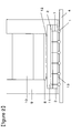
- a schematic view showing one example of the solid-state imaging device of the present invention is shown in Figure 2 .
- the solid-state imaging device has a lens holder 9 on a semiconductor substrate 3 with a solid-state imaging element 2 formed thereon, and a lens 10 and a glass 11 are caught by the lens holder 9.
- the glass 11 is formed on the solid-state imaging element 2, and an IR cut filter 8 caught by the lens holder 9 is mounted via a spacer 12.
- a solder ball 1 is formed at the tip of a through electrode 7 extending through the semiconductor substrate 3 with the solid-state imaging element 2 formed thereon, and the semiconductor substrate 3 and a mounting substrate 4 for mounting the same are connected by the solder ball 1.
- the semiconductor substrate 3 has, on the surface at the mounting substrate 4 side, a light-shielding and insulating layer 13 formed using the photosensitive resin composition of the present invention.
- the photosensitive resin composition of the present invention has insulating properties, and therefore plays a role as an insulating layer and can shield against light having a wavelength in a visible range and a near-infrared range.
- the semiconductor substrate 3 shields against light having a wavelength in an ultraviolet range and a visible range, of light incident from the semiconductor substrate 3 side to the solid-state imaging device 2, thus making it possible to shield against light having a wavelength in an ultraviolet range, a visible range and a near-infrared range.
- Measurements were made at a refraction index of 1.58 using RamdaA STM-602 manufactured by Dainippon Screen Mfg. Co. , Ltd. In the case where the film thickness was 30 ⁇ m or more, the cross section was observed with a scanning electron microscope S-4800 (manufactured by Hitachi, Ltd.) to measure the thickness.
- a photosensitive resin composition (hereinafter referred to as varnish) was applied onto a 6-inch silicon wafer so as to have a thickness of 28 ⁇ m after prebaking, and then prebaked at 100°C for 3 minutes using a hot plate (Mark-7 manufactured by Tokyo Electron Ltd.) to thereby obtain a photosensitive resin film.
- a reticle having a pattern of 150 um line-and-spaces and squares of 150 um x 150 um was set in an exposure unit (all-wavelength Stepper Spectrum 3e manufactured by Ultratech, Inc.) and the photosensitive resin film was subjected to all-wavelength exposure at an exposure amount of 1000 mJ/cm 2 (i ray equivalent).
- a 2.38 wt% aqueous tetramethylammonium hydroxide solution was sprayed to the exposed photosensitive resin film at 50 rotations for 10 seconds using a Mark-7 development apparatus manufactured by Tokyo Electron Ltd. Thereafter, it was left standing at 50 rotations for 30 seconds. This operation was repeated twice. By carrying out a rinsing treatment with water at 400 rotations and shaking-drying at 3000 rotations for 10 seconds, a post-development film was obtained.
- the post-development film was heat-treated under a nitrogen gas stream (oxygen concentration 10 ppm or less) at 180°C for 120 minutes using Inert Oven INH-21CD (Koyo Thermo Systems Co., ltd.) to obtain a cured film.
- the cross section of the cured film was observed with a scanning electron microscope S-4800 (manufactured by Hitachi, Ltd.) to determine a ratio of the length of the lower side of the cross section to the length of the upper side of the cross section (length of lower side / length of upper side) in a pattern of squares of 150 um x 150 um. If this value is 50% or more, it can be determined that the shape of a pattern is good.
- the cured film was observed with an optical microscope at 5x magnification, and presence/absence of undissolved and remaining resin composition (shallowness) on unexposed areas was evaluated in three scales.
- cured films with a thickness of 25 ⁇ m prepared on a 6-inch wafer manufactured by KST World Corp.; substrate having a wafer thickness of 625 nm and having such properties that the permeability to light having a wavelength of 400 to 900 nm inclusive is 0% and the maximum of the permeability to light having a wavelength longer than 900 nm and no longer than 1300 nm is 49.2%
- the permeability to light having a wavelength of 350 to 1400 nm was measured using a spectrophotometer UV-3150 manufactured by Shimadzu Corporation.
- the solution was introduced into 3 L of water containing 10% by weight of methanol to collect a white precipitate.
- the precipitate was collected by filtration, washed with water three times, and then dried in a vacuum drier at 50°C for 72 hours to obtain a polyhydroxyamide powder as a polybenzoxazole precursor.
- the preliminary dispersion 1 was fed into Ultra Apex Mill (manufactured by KOTOBUKI INDUSTRIES) having a centrifugal separator filled with 70% of 0.05 mm ⁇ zirconia beads (manufactured by NIKKATO CORPORATION, YTZ Ball), and dispersed at a rotation speed of 8 m/second for 2 hours to obtain a titanium nitride particle dispersion having a solid concentration of 12% by weight and a titanium nitride particle/resin (weight) ratio of 80/20.
- Ultra Apex Mill manufactured by KOTOBUKI INDUSTRIES
- a centrifugal separator filled with 70% of 0.05 mm ⁇ zirconia beads manufactured by NIKKATO CORPORATION, YTZ Ball
- a preliminary dispersion 2 was obtained in the same manner as in Synthesis Example 6 except that 96 g of titanium nitride particles (manufactured by Nisshin Engineering Inc., TiN UFP Lot 13306B10) was replaced by 96 g of carbon black ("MA 100" manufactured by Mitsubishi Kasei Kogyo Kabushiki Kaisha). Thereafter, a carbon black dispersion having a solid concentration of 12% by weight and a carbon black/resin (weight) ratio of 80/20 was obtained by carrying out dispersion for 2 hours in the same manner except that the preliminary dispersion 1 was replaced by the preliminary dispersion 2 and the rotation speed of Ultra Apex Mill was changed from 8 m/second to 8 m/20 seconds.
- OXE-02 (trade name, manufactured by Chiba Specialty Chemicals Co., Ltd.) as an oxime-type photopolymerization initiator were dissolved in 12 g of diacetone alcohol to obtain a varnish A as a photosensitive resin composition.
- a varnish A as a photosensitive resin composition.
- the pattern shape and shallowness were evaluated as described previously and the light permeabilities of a laminate and a photosensitive resin film were measured.
- a varnish B as a photosensitive resin composition was obtained in the same manner as in Example 1 except that 10.0 g of polyamide acid ester obtained in Synthesis Example 3 was used in place of the polyimide powder obtained in Synthesis Example 2. Using the obtained varnish B, evaluations were made in the same manner as in Example 1.
- a varnish C as a photosensitive resin composition was obtained in the same manner as in Example 1 except that 10.0 g of polyhydroxyamide powder obtained in Synthesis Example 4 was used in place of the polyimide powder obtained in Synthesis Example 2 and GBL was used in place of diacetone alcohol. Using the obtained varnish C, evaluations were made in the same manner as in Example 1.
- a varnish D as a photosensitive resin composition was obtained in the same manner as in Example 1 except that the added amount of YMF-02 was changed from 12.0 g to 7.5 g and GBL was used in place of diacetone alcohol. Using the obtained varnish D, evaluations were made in the same manner as in Example 1.
- a varnish E as a photosensitive resin composition was obtained in the same manner as in Example 1 except that the added amount of YMF-02 (trade name, manufactured by Sumitomo Metal Mining Co., Ltd.) was changed from 12. 0 g to 17.5 g. Using the obtained varnish E, evaluations were made in the same manner as in Example 1.
- a varnish F as a photosensitive resin composition was obtained in the same manner as in Example 1 except that 2.4 g of CsWO012-3 (trade name, manufactured by NanoGram Corporation, Cs0 .4 WO 3 ) was used in place of 12.0 g of YMF-02 (trade name, manufactured by Sumitomo Metal Mining Co., Ltd.). Using the obtained varnish F, evaluations were made in the same manner as in Example 1.
- a varnish G as a photosensitive resin composition was obtained in the same manner as in Example 1 except that 3.0 g of MX-270 (trade name, manufactured by Midori Kagaku Co. , Ltd.) was further used and 12. 0 g of GBL was used in place of diacetone alcohol. Using the obtained varnish G, evaluations were made in the same manner as in Example 1.
- a varnish H as a photosensitive resin composition was obtained in the same manner as in Example 1 except that 2.4 g of CsWO009-04 (trade name, manufactured by NanoGram Corporation, Cs 0.1 WO 3 ) was used in place of 12.0 g of YMF-02 (trade name, manufactured by Sumitomo Metal Mining Co., Ltd.). Using the obtained varnish H, evaluations were made in the same manner as in Example 1.
- a varnish J as a photosensitive resin composition was obtained in the same manner as in Example 9 except that 10.0 g of polyamide acid ester obtained in Synthesis Example 3 was used in place of the polyimide powder obtained in Synthesis Example 2. Using the obtained varnish J, evaluations were made in the same manner as in Example 1.
- a varnish K as a photosensitive resin composition was obtained in the same manner as in Example 9 except that 10.0 g of polyhydroxyamide powder obtained in Synthesis Example 4 were used in place of the polyimide powder obtained in Synthesis Example 2 and the added amount of PDBE-250 (trade name, manufactured by NOF CORPORATION) was changed from 4.8 g to 3.0 g, 3.0 g of DCP-A was used in place of 1.2 g of MOI-BP (trade name, manufactured by Showa Denko K.K.) and GBL was used in place of diacetone alcohol. Using the obtained varnish K, evaluations were made in the same manner as in Example 1.
- a varnish L as a photosensitive resin composition was obtained in the same manner as in Example 9 except that the added amount of YMF-02 (trade name, manufactured by Sumitomo Metal Mining Co., Ltd.) was changed from 12.0 g to 7.5 g and GBL was used in place of diacetone alcohol. Using the obtained varnish L, evaluations were made in the same manner as in Example 1.
- YMF-02 trade name, manufactured by Sumitomo Metal Mining Co., Ltd.
- a varnish M as a photosensitive resin composition was obtained in the same manner as in Example 9 except that the added amount of YMF-02 (trade name, manufactured by Sumitomo Metal Mining Co., Ltd.) was changed from 12.0 g to 17.5 g. Using the obtained varnish M, evaluations were made in the same manner as in Example 1.
- a varnish N as a photosensitive resin composition was obtained in the same manner as in Example 9 except that the added amount of PDBE-250 (trade name, manufactured by NOF CORPORATION) was changed from 4. 8 g to 5.4 g and the added amount of MOI-BP (trade name, manufactured by Showa Denko K.K.) was changed from 1.2 g to 0.6 g. Using the obtained varnish N, evaluations were made in the same manner as in Example 1.
- a varnish O as a photosensitive resin composition was obtained in the same manner as in Example 9 except that 4.8 g of pentaerythritol triacrylate were used as a photopolymerizable compound having three polymerizable groups, in place of PDBE-250 (trade name, manufactured by NOF CORPORATION). Using the obtained varnish O, evaluations were made in the same manner as in Example 1.
- a varnish P as a photosensitive resin composition was obtained in the same manner as in Example 9 except that 2.4 g of CsWO012-3 (trade name, manufactured by NanoGram Corporation, Cs 0.4 WO 3 ) was used in place of 12.0 g of YMF-02 (trade name, manufactured by Sumitomo Metal Mining Co., Ltd.). Using the obtained varnish P, evaluations were made in the same manner as in Example 1.
- a varnish Q as a photosensitive resin composition was obtained in the same manner as in Example 9 except that 2.4 g of CsWO009-04 (trade name, manufactured by NanoGram Corporation, Cs 0.1 WO 3 ) was used in place of 12.0 g of YMF-02 (trade name, manufactured by Sumitomo Metal Mining Co., Ltd.). Using the obtained varnish Q, evaluations were made in the same manner as in Example 1.
- a varnish R as a photosensitive resin composition was obtained in the same manner as in Example 9 except that 3.0 g of MX-270 (trade name, manufactured by Midori Kagaku Co., Ltd.) was further used and 12. 0 g of GBL were used in place of diacetone alcohol. Using the obtained varnish R, evaluations were made in the same manner as in Example 1.
- a varnish S as a photosensitive resin composition was obtained in the same manner as in Example 9 except that the added amount of YMF-02 (trade name, manufactured by Sumitomo Metal Mining Co., Ltd.) was changed from 12. 0 g to 15.0 g and the added amount of OXE-02 (trade name, manufactured by Chiba Specialty Chemicals Co., Ltd.) was changed from 2.0 g to 0.7 g.
- YMF-02 trade name, manufactured by Sumitomo Metal Mining Co., Ltd.
- OXE-02 trade name, manufactured by Chiba Specialty Chemicals Co., Ltd.
- a photosensitive resin composition T was obtained in the same manner as in Example 9 except that MOI-BP (trade name, manufactured by Showa Denko K.K.) was not used and the added amount of PDBE-250 (trade name, manufactured by NOF CORPORATION) was changed from 4.8 g to 6 g. Using the obtained varnish T, evaluations were made in the same manner as in Example 1.
- MOI-BP trade name, manufactured by Showa Denko K.K.
- PDBE-250 trade name, manufactured by NOF CORPORATION
- a varnish U as a photosensitive resin composition was obtained in the same manner as in Example 1 except that 12.0 g of YMF-02 (trade name, manufactured by Sumitomo Metal Mining Co., Ltd.) was not included. Using the obtained varnish U, evaluations were made in the same manner as in Example 1.
- a varnish V as a photosensitive resin composition was obtained in the same manner as in Example 1 except that 2.4 g of titanium nitride particle dispersion obtained in Synthesis Example 6 was used in place of YMF-02 (trade name, manufactured by Sumitomo Metal Mining Co. , Ltd.). Using the obtained varnish V, evaluations were made in the same manner as in Example 1.
- a varnish W as a photosensitive resin composition was obtained in the same manner as in Example 1 except that 2.4 g of carbon black dispersion obtained in Synthesis Example 7 was used in place of YMF-02 (trade name, manufactured by Sumitomo Metal Mining Co., Ltd.). Using the obtained varnish W, evaluations were made in the same manner as in Example 1.
- a varnish X as a photosensitive resin composition was obtained in the same manner as in Example 9 except that YMF-02 (trade name, manufactured by Sumitomo Metal Mining Co., Ltd.) was not contained. Using the obtained varnish X, evaluations were made in the same manner as in Example 1.
- a varnish Y as a photosensitive resin composition was obtained in the same manner as in Example 9 except that 25 g of titanium nitride particle dispersion 1 obtained in Synthesis Example 6 was used in place of YMF-02 (trade name, manufactured by Sumitomo Metal Mining Co., Ltd.). Using the obtained varnish Y, evaluations were made in the same manner as in Example 1.
- a varnish Z as a photosensitive resin composition was obtained in the same manner as in Example 9 except that 25 g of carbon black dispersion 2 obtained in Synthesis Example 7 was used in place of YMF-02 (trade name, manufactured by Sumitomo Metal Mining Co., Ltd.). Using the obtained varnish Z, evaluations were made in the same manner as in Example 1.
- a varnish AA as a photosensitive resin composition was obtained in the same manner as in Example 9 except that PDBE-250 (trade name, manufactured by NOF CORPORATION) was not used and the added amount of MOI-BP (trade name, manufactured by Showa Denko K.K.) was changed from 1.2 g to 6 g. Using the obtained varnish AA, evaluations were made in the same manner as in Example 1.
- a varnish AB as a photosensitive resin composition was obtained in the same manner as in Example 9 except that no polyimide powder was used, 10 g of pentaerythritol tetraacrylate was used in place of PDBE-250 (trade name, manufactured by NOF CORPORATION) and MOI-BP (trade name, manufactured by Showa Denko K.K.), and 0.3 g of Irgacure 907 (trade name, manufactured by Chiba Specialty Chemicals Co., Ltd.) was used in place of OXE-02 (trade name, manufactured by Chiba Specialty Chemicals Co., Ltd.). Using the obtained varnish AB, evaluations were made in the same manner as in Example 1.
- Example 2 Using the varnish A obtained in Example 1, evaluations were made in the same manner as in Example 1 except that a TEMPAX glass plate (permeability to light having a wavelength of 400 to 1300 nm: 100%) was used as a substrate.
- a TEMPAX glass plate permeability to light having a wavelength of 400 to 1300 nm: 100%
- compositions of the photosensitive resin compositions of Examples, Comparative Examples and Reference Example are shown in Tables 1 to 3 and the evaluation results are shown in Tables 4 to 6.
- Insulating properties and light-shielding properties against light having a wavelength lying in an ultraviolet range, a visible range and a near-infrared range can be imparted by applying a photosensitive resin composition of the present invention onto a substrate which has such properties that the permeability to light having a wavelength of 400 to 900 nm inclusive is less than 3.0% and the maximum value of the permeability to light having a wavelength longer than 900 nm and no longer than 1300 nm is 3.0% or more. Accordingly, a solid-state imaging device can be provided using a simpler and more productive method.
Landscapes
- Physics & Mathematics (AREA)
- General Physics & Mathematics (AREA)
- Spectroscopy & Molecular Physics (AREA)
- Engineering & Computer Science (AREA)
- Architecture (AREA)
- Structural Engineering (AREA)
- Chemical & Material Sciences (AREA)
- Organic Chemistry (AREA)
- Materials For Photolithography (AREA)
- Electromagnetism (AREA)
- Macromonomer-Based Addition Polymer (AREA)
Applications Claiming Priority (2)
| Application Number | Priority Date | Filing Date | Title |
|---|---|---|---|
| JP2009276101 | 2009-12-04 | ||
| PCT/JP2010/068939 WO2011067998A1 (fr) | 2009-12-04 | 2010-10-26 | Composition de résine photosensible, stratifié l'utilisant et dispositif d'imagerie à l'état solide |
Publications (2)
| Publication Number | Publication Date |
|---|---|
| EP2508947A1 true EP2508947A1 (fr) | 2012-10-10 |
| EP2508947A4 EP2508947A4 (fr) | 2013-12-11 |
Family
ID=44114856
Family Applications (1)
| Application Number | Title | Priority Date | Filing Date |
|---|---|---|---|
| EP10834451.6A Withdrawn EP2508947A4 (fr) | 2009-12-04 | 2010-10-26 | Composition de résine photosensible, stratifié l'utilisant et dispositif d'imagerie à l'état solide |
Country Status (9)
| Country | Link |
|---|---|
| US (1) | US8901225B2 (fr) |
| EP (1) | EP2508947A4 (fr) |
| JP (1) | JP5088419B2 (fr) |
| KR (2) | KR101913997B1 (fr) |
| CN (1) | CN102640054B (fr) |
| MY (1) | MY163409A (fr) |
| SG (1) | SG181464A1 (fr) |
| TW (1) | TWI510859B (fr) |
| WO (1) | WO2011067998A1 (fr) |
Cited By (2)
| Publication number | Priority date | Publication date | Assignee | Title |
|---|---|---|---|---|
| WO2011145742A1 (fr) | 2010-05-19 | 2011-11-24 | Fujifilm Corporation | Composition polymérisable |
| WO2012015076A1 (fr) | 2010-07-29 | 2012-02-02 | Fujifilm Corporation | Composition polymérisable |
Families Citing this family (26)
| Publication number | Priority date | Publication date | Assignee | Title |
|---|---|---|---|---|
| JP2012003225A (ja) | 2010-01-27 | 2012-01-05 | Fujifilm Corp | ソルダーレジスト用重合性組成物及びソルダーレジストパターンの形成方法 |
| JP5544217B2 (ja) * | 2010-05-19 | 2014-07-09 | 富士フイルム株式会社 | 重合性組成物 |
| JP5674399B2 (ja) * | 2010-09-22 | 2015-02-25 | 富士フイルム株式会社 | 重合性組成物、感光層、永久パターン、ウエハレベルレンズ、固体撮像素子、及び、パターン形成方法 |
| JP5588847B2 (ja) * | 2010-11-30 | 2014-09-10 | 富士フイルム株式会社 | 重合性組成物、並びに、これを用いた感光層、永久パターン、ウエハレベルレンズ、固体撮像素子、及び、パターン形成方法 |
| JP5417364B2 (ja) * | 2011-03-08 | 2014-02-12 | 富士フイルム株式会社 | 固体撮像素子用硬化性組成物、並びに、これを用いた感光層、永久パターン、ウエハレベルレンズ、固体撮像素子、及び、パターン形成方法 |
| JP5879088B2 (ja) * | 2011-10-14 | 2016-03-08 | 旭化成イーマテリアルズ株式会社 | 感光性樹脂組成物、及び、硬化レリーフパターンの製造方法 |
| JP5896685B2 (ja) * | 2011-10-21 | 2016-03-30 | スリーエム イノベイティブ プロパティズ カンパニー | 熱遮蔽用積層体及びその製造に用いられる積層フィルム |
| US9331219B2 (en) | 2012-05-11 | 2016-05-03 | Nxp, B.V. | Integrated circuit with directional light sensor, device including such an IC and method of manufacturing such an IC |
| EP2662895B1 (fr) * | 2012-05-11 | 2014-06-25 | Nxp B.V. | Circuit intégré comprenant un capteur de lumière directionnelle |
| CN104662475B (zh) | 2012-09-25 | 2019-03-29 | 东丽株式会社 | 正型感光性树脂组合物、含有使用了其的固化膜的半导体器件的制造方法 |
| WO2015011893A1 (fr) * | 2013-07-23 | 2015-01-29 | 日立化成デュポンマイクロシステムズ株式会社 | Composition de résine, procédé de formation d'un motif en l'utilisant, et composant électronique |
| JP6408802B2 (ja) * | 2014-06-27 | 2018-10-17 | 東京応化工業株式会社 | 感エネルギー性樹脂組成物 |
| JP6326142B2 (ja) | 2014-09-01 | 2018-05-16 | 富士フイルム株式会社 | 赤外光遮蔽組成物、赤外光カットフィルタ、固体撮像素子 |
| KR102510370B1 (ko) * | 2014-10-06 | 2023-03-17 | 도레이 카부시키가이샤 | 수지 조성물, 내열성 수지막의 제조 방법, 및 표시 장치 |
| JP6577176B2 (ja) * | 2014-10-14 | 2019-09-18 | 旭化成株式会社 | ネガ型感光性樹脂組成物及び転写材料 |
| TWI675907B (zh) * | 2015-01-21 | 2019-11-01 | 日商Jsr股份有限公司 | 固體攝像裝置 |
| JP6541400B2 (ja) * | 2015-04-13 | 2019-07-10 | 共同印刷株式会社 | 偽造防止用インキ及びその印刷物 |
| JP6434633B2 (ja) * | 2015-08-31 | 2018-12-05 | 富士フイルム株式会社 | 感光性樹脂組成物、平版印刷版原版及び平版印刷版の製版方法 |
| WO2017053401A1 (fr) * | 2015-09-25 | 2017-03-30 | 3M Innovative Properties Company | Encre d'impression durcissable absorbant la lumière infrarouge et articles préparés avec cette dernière |
| SG11201802076PA (en) * | 2015-09-30 | 2018-04-27 | Toray Industries | Negative photosensitive resin composition, cured film, element and display device each provided with cured film, and method for manufacturing display device |
| KR102404323B1 (ko) * | 2017-04-25 | 2022-06-07 | 삼성전기주식회사 | 차광성 수지 조성물 및 이를 포함하는 성형품 |
| JPWO2019026772A1 (ja) * | 2017-07-31 | 2020-07-02 | 太陽ホールディングス株式会社 | 感光性樹脂組成物、ドライフィルム、硬化物、プリント配線板、半導体素子および電子部品 |
| KR20200055715A (ko) * | 2017-09-29 | 2020-05-21 | 도레이 카부시키가이샤 | 감광성 수지 조성물, 경화막, 경화막을 구비하는 소자 및 유기 el 디스플레이, 그리고 유기 el 디스플레이의 제조 방법 |
| JP7331860B2 (ja) * | 2018-10-15 | 2023-08-23 | 日産化学株式会社 | 感光性絶縁膜組成物 |
| WO2021117586A1 (fr) * | 2019-12-11 | 2021-06-17 | 日産化学株式会社 | Composition filmogène isolante photosensible |
| CN117545185A (zh) * | 2023-11-22 | 2024-02-09 | 宏锐兴(湖北)电子有限责任公司 | 一种激光雷达芯片载板制造工艺方法 |
Family Cites Families (18)
| Publication number | Priority date | Publication date | Assignee | Title |
|---|---|---|---|---|
| JPH04111353A (ja) * | 1990-08-31 | 1992-04-13 | Canon Inc | 光電変換装置 |
| US6546939B1 (en) * | 1990-11-05 | 2003-04-15 | Ekc Technology, Inc. | Post clean treatment |
| JPH06251621A (ja) * | 1993-02-26 | 1994-09-09 | Toray Ind Inc | 感光性誘電ペースト |
| JPH09208775A (ja) | 1996-01-30 | 1997-08-12 | Kureha Chem Ind Co Ltd | 塩化ビニル系樹脂組成物 |
| JP3937851B2 (ja) | 2002-02-01 | 2007-06-27 | 住友金属鉱山株式会社 | プラズマディスプレイパネル用近赤外線吸収フィルター |
| JP4586970B2 (ja) | 2004-11-30 | 2010-11-24 | 住友金属鉱山株式会社 | プラズマディスプレイパネル用近赤外線吸収フィルター、及びこれを用いたプラズマディスプレイパネル |
| JP2006309202A (ja) * | 2005-03-29 | 2006-11-09 | Toray Ind Inc | 感光性樹脂組成物およびそれを用いた半導体装置 |
| JP4826415B2 (ja) * | 2005-10-12 | 2011-11-30 | 東レ株式会社 | 感光性樹脂組成物 |
| KR101286101B1 (ko) * | 2006-03-28 | 2013-07-15 | 후지필름 가부시키가이샤 | 감광성 조성물, 감광성 필름, 영구 패턴 형성방법, 및 프린트 기판 |
| JP4950542B2 (ja) | 2006-04-07 | 2012-06-13 | 岩手東芝エレクトロニクス株式会社 | 固体撮像装置およびその製造方法 |
| JP4753040B2 (ja) | 2006-09-21 | 2011-08-17 | 日産化学工業株式会社 | 重合性基を有する化合物を含有するネガ型感光性樹脂組成物 |
| JP5109553B2 (ja) * | 2006-09-27 | 2012-12-26 | 東レ株式会社 | 感光性樹脂組成物およびそれを用いた誘電体組成物、半導体装置 |
| KR20080036771A (ko) * | 2006-10-24 | 2008-04-29 | 삼성전자주식회사 | 유기층 패턴 형성방법, 그에 의해 형성된 유기층 및 그를포함하는 유기 메모리 소자 |
| JP2008311280A (ja) | 2007-06-12 | 2008-12-25 | Iwate Toshiba Electronics Co Ltd | カメラモジュールおよびその製造方法 |
| JP5287080B2 (ja) * | 2007-10-18 | 2013-09-11 | 日油株式会社 | プラズマディスプレイパネル用ハードコートフィルム及びプラズマディスプレイパネル |
| JP5358976B2 (ja) * | 2008-02-29 | 2013-12-04 | 大日本印刷株式会社 | 近赤外線吸収材 |
| JP5344843B2 (ja) * | 2008-03-31 | 2013-11-20 | 富士フイルム株式会社 | 重合性組成物および固体撮像素子 |
| JP5544239B2 (ja) * | 2010-07-29 | 2014-07-09 | 富士フイルム株式会社 | 重合性組成物 |
-
2010
- 2010-10-26 KR KR1020177036813A patent/KR101913997B1/ko not_active Expired - Fee Related
- 2010-10-26 US US13/513,464 patent/US8901225B2/en not_active Expired - Fee Related
- 2010-10-26 EP EP10834451.6A patent/EP2508947A4/fr not_active Withdrawn
- 2010-10-26 JP JP2010545713A patent/JP5088419B2/ja not_active Expired - Fee Related
- 2010-10-26 MY MYPI2012002447A patent/MY163409A/en unknown
- 2010-10-26 SG SG2012040325A patent/SG181464A1/en unknown
- 2010-10-26 WO PCT/JP2010/068939 patent/WO2011067998A1/fr not_active Ceased
- 2010-10-26 KR KR1020127013779A patent/KR20120109489A/ko not_active Ceased
- 2010-10-26 CN CN201080055022.8A patent/CN102640054B/zh not_active Expired - Fee Related
- 2010-12-03 TW TW099142020A patent/TWI510859B/zh not_active IP Right Cessation
Cited By (6)
| Publication number | Priority date | Publication date | Assignee | Title |
|---|---|---|---|---|
| WO2011145742A1 (fr) | 2010-05-19 | 2011-11-24 | Fujifilm Corporation | Composition polymérisable |
| EP2572243A4 (fr) * | 2010-05-19 | 2014-01-22 | Fujifilm Corp | Composition polymérisable |
| US8735483B2 (en) | 2010-05-19 | 2014-05-27 | Fujifilm Corporation | Polymerizable composition |
| WO2012015076A1 (fr) | 2010-07-29 | 2012-02-02 | Fujifilm Corporation | Composition polymérisable |
| EP2598946A4 (fr) * | 2010-07-29 | 2014-05-07 | Fujifilm Corp | Composition polymérisable |
| US8728712B2 (en) | 2010-07-29 | 2014-05-20 | Fujifilm Corporation | Polymerizable composition |
Also Published As
| Publication number | Publication date |
|---|---|
| KR20120109489A (ko) | 2012-10-08 |
| JP5088419B2 (ja) | 2012-12-05 |
| SG181464A1 (en) | 2012-07-30 |
| EP2508947A4 (fr) | 2013-12-11 |
| US8901225B2 (en) | 2014-12-02 |
| KR20180001577A (ko) | 2018-01-04 |
| CN102640054A (zh) | 2012-08-15 |
| JPWO2011067998A1 (ja) | 2013-04-18 |
| US20120244473A1 (en) | 2012-09-27 |
| KR101913997B1 (ko) | 2018-10-31 |
| TW201129867A (en) | 2011-09-01 |
| CN102640054B (zh) | 2013-07-24 |
| WO2011067998A1 (fr) | 2011-06-09 |
| MY163409A (en) | 2017-09-15 |
| TWI510859B (zh) | 2015-12-01 |
Similar Documents
| Publication | Publication Date | Title |
|---|---|---|
| EP2508947A1 (fr) | Composition de résine photosensible, stratifié l'utilisant et dispositif d'imagerie à l'état solide | |
| JP5211438B2 (ja) | 樹脂組成物およびそれを用いた表示装置 | |
| EP2520977B1 (fr) | Composition de résine photosensible de type positif | |
| KR100766648B1 (ko) | 포지티브형 감광성 수지 조성물,포지티브형 감광성 수지조성물의 제조방법 및 반도체장치 | |
| KR20190125983A (ko) | 감광성 수지 조성물, 경화막, 경화막을 구비하는 소자, 경화막을 구비하는 유기 el 표시 장치, 경화막의 제조 방법, 및 유기 el 표시 장치의 제조 방법 | |
| JPWO2017169574A1 (ja) | 感光性接着剤組成物、硬化物、感光性接着剤シート、積層基板および接着剤パターン付積層基板の製造方法 | |
| EP2902846B1 (fr) | Composition de résine photosensible positive | |
| CN108885401A (zh) | 感光性树脂组合物 | |
| CN108368263B (zh) | 树脂、浆料、以及使用其得到的层叠体和其制造方法 | |
| JP7131133B2 (ja) | 樹脂組成物 | |
| WO2017217293A1 (fr) | Composition de résine photosensible | |
| KR20190120710A (ko) | 네거티브형 감광성 수지 조성물 및 경화 릴리프 패턴의 제조 방법 | |
| TW202039638A (zh) | 負型感光性樹脂組合物、聚醯亞胺之製造方法及硬化浮凸圖案之製造方法 | |
| CN117836352A (zh) | 聚酰亚胺树脂、感光性树脂组合物、固化物、有机el显示器、电子部件及半导体装置 | |
| JP2008281597A (ja) | 感光性樹脂組成物シート | |
| JP3995962B2 (ja) | ポジ型感光性樹脂組成物及び半導体装置 | |
| CN102713753A (zh) | 正型感光性树脂组合物、图形固化膜的制造方法以及电子部件 | |
| JP5115045B2 (ja) | ポリイミドワニス | |
| JP2010210851A (ja) | 感光性樹脂組成物 | |
| JP5407163B2 (ja) | ペースト組成物およびそれを用いた高熱伝導率樹脂組成物 | |
| JP5875209B2 (ja) | 熱硬化性樹脂組成物 | |
| JP2009227697A (ja) | 架橋剤およびそれを用いた感光性樹脂組成物 | |
| JP2022022578A (ja) | 樹脂組成物、硬化膜、硬化膜の製造方法、半導体装置および有機el表示装置 | |
| JP7559983B1 (ja) | 感光性樹脂組成物、硬化物、有機el表示装置、電子部品、および半導体装置 | |
| JP7711749B2 (ja) | 硬化膜付きled実装基板の製造方法 |
Legal Events
| Date | Code | Title | Description |
|---|---|---|---|
| PUAI | Public reference made under article 153(3) epc to a published international application that has entered the european phase |
Free format text: ORIGINAL CODE: 0009012 |
|
| 17P | Request for examination filed |
Effective date: 20120515 |
|
| AK | Designated contracting states |
Kind code of ref document: A1 Designated state(s): AL AT BE BG CH CY CZ DE DK EE ES FI FR GB GR HR HU IE IS IT LI LT LU LV MC MK MT NL NO PL PT RO RS SE SI SK SM TR |
|
| DAX | Request for extension of the european patent (deleted) | ||
| A4 | Supplementary search report drawn up and despatched |
Effective date: 20131111 |
|
| RIC1 | Information provided on ipc code assigned before grant |
Ipc: G03F 7/004 20060101AFI20131105BHEP Ipc: G03F 7/09 20060101ALI20131105BHEP Ipc: G03F 7/037 20060101ALI20131105BHEP Ipc: G03F 7/031 20060101ALI20131105BHEP Ipc: H01L 27/14 20060101ALI20131105BHEP |
|
| 17Q | First examination report despatched |
Effective date: 20170418 |
|
| GRAP | Despatch of communication of intention to grant a patent |
Free format text: ORIGINAL CODE: EPIDOSNIGR1 |
|
| INTG | Intention to grant announced |
Effective date: 20171220 |
|
| STAA | Information on the status of an ep patent application or granted ep patent |
Free format text: STATUS: THE APPLICATION IS DEEMED TO BE WITHDRAWN |
|
| 18D | Application deemed to be withdrawn |
Effective date: 20180501 |