EP2509120A1 - Halbleiterbauelement und -verfahren - Google Patents
Halbleiterbauelement und -verfahren Download PDFInfo
- Publication number
- EP2509120A1 EP2509120A1 EP12162196A EP12162196A EP2509120A1 EP 2509120 A1 EP2509120 A1 EP 2509120A1 EP 12162196 A EP12162196 A EP 12162196A EP 12162196 A EP12162196 A EP 12162196A EP 2509120 A1 EP2509120 A1 EP 2509120A1
- Authority
- EP
- European Patent Office
- Prior art keywords
- layer
- pattern
- substrate
- iii
- range
- Prior art date
- Legal status (The legal status is an assumption and is not a legal conclusion. Google has not performed a legal analysis and makes no representation as to the accuracy of the status listed.)
- Withdrawn
Links
Images


Classifications
-
- H—ELECTRICITY
- H10—SEMICONDUCTOR DEVICES; ELECTRIC SOLID-STATE DEVICES NOT OTHERWISE PROVIDED FOR
- H10P—GENERIC PROCESSES OR APPARATUS FOR THE MANUFACTURE OR TREATMENT OF DEVICES COVERED BY CLASS H10
- H10P14/00—Formation of materials, e.g. in the shape of layers or pillars
- H10P14/20—Formation of materials, e.g. in the shape of layers or pillars of semiconductor materials
- H10P14/32—Formation of materials, e.g. in the shape of layers or pillars of semiconductor materials characterised by intermediate layers between substrates and deposited layers
- H10P14/3242—Structure
-
- H—ELECTRICITY
- H10—SEMICONDUCTOR DEVICES; ELECTRIC SOLID-STATE DEVICES NOT OTHERWISE PROVIDED FOR
- H10P—GENERIC PROCESSES OR APPARATUS FOR THE MANUFACTURE OR TREATMENT OF DEVICES COVERED BY CLASS H10
- H10P14/00—Formation of materials, e.g. in the shape of layers or pillars
- H10P14/20—Formation of materials, e.g. in the shape of layers or pillars of semiconductor materials
- H10P14/29—Formation of materials, e.g. in the shape of layers or pillars of semiconductor materials characterised by the substrates
- H10P14/2901—Materials
-
- H—ELECTRICITY
- H10—SEMICONDUCTOR DEVICES; ELECTRIC SOLID-STATE DEVICES NOT OTHERWISE PROVIDED FOR
- H10P—GENERIC PROCESSES OR APPARATUS FOR THE MANUFACTURE OR TREATMENT OF DEVICES COVERED BY CLASS H10
- H10P14/00—Formation of materials, e.g. in the shape of layers or pillars
- H10P14/20—Formation of materials, e.g. in the shape of layers or pillars of semiconductor materials
- H10P14/29—Formation of materials, e.g. in the shape of layers or pillars of semiconductor materials characterised by the substrates
- H10P14/2901—Materials
- H10P14/2902—Materials being Group IVA materials
- H10P14/2905—Silicon, silicon germanium or germanium
-
- H—ELECTRICITY
- H10—SEMICONDUCTOR DEVICES; ELECTRIC SOLID-STATE DEVICES NOT OTHERWISE PROVIDED FOR
- H10P—GENERIC PROCESSES OR APPARATUS FOR THE MANUFACTURE OR TREATMENT OF DEVICES COVERED BY CLASS H10
- H10P14/00—Formation of materials, e.g. in the shape of layers or pillars
- H10P14/20—Formation of materials, e.g. in the shape of layers or pillars of semiconductor materials
- H10P14/29—Formation of materials, e.g. in the shape of layers or pillars of semiconductor materials characterised by the substrates
- H10P14/2924—Structures
- H10P14/2925—Surface structures
-
- H—ELECTRICITY
- H10—SEMICONDUCTOR DEVICES; ELECTRIC SOLID-STATE DEVICES NOT OTHERWISE PROVIDED FOR
- H10P—GENERIC PROCESSES OR APPARATUS FOR THE MANUFACTURE OR TREATMENT OF DEVICES COVERED BY CLASS H10
- H10P14/00—Formation of materials, e.g. in the shape of layers or pillars
- H10P14/20—Formation of materials, e.g. in the shape of layers or pillars of semiconductor materials
- H10P14/32—Formation of materials, e.g. in the shape of layers or pillars of semiconductor materials characterised by intermediate layers between substrates and deposited layers
- H10P14/3202—Materials thereof
- H10P14/3214—Materials thereof being Group IIIA-VA semiconductors
- H10P14/3216—Nitrides
-
- H—ELECTRICITY
- H10—SEMICONDUCTOR DEVICES; ELECTRIC SOLID-STATE DEVICES NOT OTHERWISE PROVIDED FOR
- H10P—GENERIC PROCESSES OR APPARATUS FOR THE MANUFACTURE OR TREATMENT OF DEVICES COVERED BY CLASS H10
- H10P14/00—Formation of materials, e.g. in the shape of layers or pillars
- H10P14/20—Formation of materials, e.g. in the shape of layers or pillars of semiconductor materials
- H10P14/32—Formation of materials, e.g. in the shape of layers or pillars of semiconductor materials characterised by intermediate layers between substrates and deposited layers
- H10P14/3242—Structure
- H10P14/3244—Layer structure
- H10P14/3251—Layer structure consisting of three or more layers
-
- H—ELECTRICITY
- H10—SEMICONDUCTOR DEVICES; ELECTRIC SOLID-STATE DEVICES NOT OTHERWISE PROVIDED FOR
- H10P—GENERIC PROCESSES OR APPARATUS FOR THE MANUFACTURE OR TREATMENT OF DEVICES COVERED BY CLASS H10
- H10P14/00—Formation of materials, e.g. in the shape of layers or pillars
- H10P14/20—Formation of materials, e.g. in the shape of layers or pillars of semiconductor materials
- H10P14/32—Formation of materials, e.g. in the shape of layers or pillars of semiconductor materials characterised by intermediate layers between substrates and deposited layers
- H10P14/3258—Crystal orientation
-
- H—ELECTRICITY
- H10—SEMICONDUCTOR DEVICES; ELECTRIC SOLID-STATE DEVICES NOT OTHERWISE PROVIDED FOR
- H10P—GENERIC PROCESSES OR APPARATUS FOR THE MANUFACTURE OR TREATMENT OF DEVICES COVERED BY CLASS H10
- H10P14/00—Formation of materials, e.g. in the shape of layers or pillars
- H10P14/20—Formation of materials, e.g. in the shape of layers or pillars of semiconductor materials
- H10P14/34—Deposited materials, e.g. layers
- H10P14/3402—Deposited materials, e.g. layers characterised by the chemical composition
- H10P14/3414—Deposited materials, e.g. layers characterised by the chemical composition being group IIIA-VIA materials
- H10P14/3416—Nitrides
-
- H—ELECTRICITY
- H10—SEMICONDUCTOR DEVICES; ELECTRIC SOLID-STATE DEVICES NOT OTHERWISE PROVIDED FOR
- H10P—GENERIC PROCESSES OR APPARATUS FOR THE MANUFACTURE OR TREATMENT OF DEVICES COVERED BY CLASS H10
- H10P14/00—Formation of materials, e.g. in the shape of layers or pillars
- H10P14/20—Formation of materials, e.g. in the shape of layers or pillars of semiconductor materials
- H10P14/34—Deposited materials, e.g. layers
- H10P14/3451—Structure
-
- H—ELECTRICITY
- H10—SEMICONDUCTOR DEVICES; ELECTRIC SOLID-STATE DEVICES NOT OTHERWISE PROVIDED FOR
- H10H—INORGANIC LIGHT-EMITTING SEMICONDUCTOR DEVICES HAVING POTENTIAL BARRIERS
- H10H20/00—Individual inorganic light-emitting semiconductor devices having potential barriers, e.g. light-emitting diodes [LED]
- H10H20/01—Manufacture or treatment
- H10H20/011—Manufacture or treatment of bodies, e.g. forming semiconductor layers
- H10H20/013—Manufacture or treatment of bodies, e.g. forming semiconductor layers having light-emitting regions comprising only Group III-V materials
- H10H20/0133—Manufacture or treatment of bodies, e.g. forming semiconductor layers having light-emitting regions comprising only Group III-V materials with a substrate not being Group III-V materials
- H10H20/01335—Manufacture or treatment of bodies, e.g. forming semiconductor layers having light-emitting regions comprising only Group III-V materials with a substrate not being Group III-V materials the light-emitting regions comprising nitride materials
-
- H—ELECTRICITY
- H10—SEMICONDUCTOR DEVICES; ELECTRIC SOLID-STATE DEVICES NOT OTHERWISE PROVIDED FOR
- H10H—INORGANIC LIGHT-EMITTING SEMICONDUCTOR DEVICES HAVING POTENTIAL BARRIERS
- H10H20/00—Individual inorganic light-emitting semiconductor devices having potential barriers, e.g. light-emitting diodes [LED]
- H10H20/80—Constructional details
- H10H20/81—Bodies
- H10H20/811—Bodies having quantum effect structures or superlattices, e.g. tunnel junctions
- H10H20/812—Bodies having quantum effect structures or superlattices, e.g. tunnel junctions within the light-emitting regions, e.g. having quantum confinement structures
Definitions
- the invention relates to the field of semiconductor devices with at least one potential-jump barrier or surface barrier specially adapted for light emission and a process specially adapted for the manufacture or treatment thereof or of parts thereof.
- Assemblies consisting of a plurality of individual semiconductor devices and including semiconductor devices with at least one potential-jump barrier or surface barrier, specially adapted for light emission, are known.
- electroluminescent light sources in general, circuit arrangements for light emitting diodes and electric lamps using semiconductor devices as light generating elements are known.
- Group III-nitride-based light-emitting diodes are expected to be employed in display and general lighting applications, replacing conventional incandescent and fluorescent lighting sources in near future due to their inherent higher energy efficiency and longer lifetime.
- One of the critical technical challenges to be addressed for high-brightness and high-power operations of LEDs is a phenomenon commonly referred to as an efficiency droop, which is observed as a reduction in emission efficiency with increasing injection current under high current density conditions.
- efficiency droop One of the critical technical challenges to be addressed for high-brightness and high-power operations of LEDs is a phenomenon commonly referred to as an efficiency droop, which is observed as a reduction in emission efficiency with increasing injection current under high current density conditions.
- good LED shows maximum quantum efficiency at 10-20 mA/cm 2 and the efficiency continuously decreases at high current density, which is a so called efficiency droop.
- Efficiency-droop is a main bottleneck to achieve a high power and high efficiency LED.
- a high power LED needs to operate at 350mA or even at 1A.
- a large LED chip has a feature size of 1x1 mm 2 whereas small ones are only 300x300 ⁇ m 2 .
- a current density will be 35 and 100 A/cm 2 , respectively. At such a high current density level, quantum efficiency is significantly reduced.
- US 2010264454 (A1 ) recites that at least partial strain relief in a light emitting layer of a III-nitride light emitting device is provided by configuring the surface on which at least one layer of the device grows such that the layer expands laterally and thus at least partially relaxes.
- This layer is referred to as the strain-relieved layer.
- the light emitting layer itself is the strain-relieved layer, meaning that the light emitting layer is grown on a surface that allows the light emitting layer to expand laterally to relieve strain.
- a layer grown before the light emitting layer is the strain-relieved layer.
- the strain-relieved layer is grown on a textured surface.
- the above document recites provision of a textured, non regular structure, which is only provided within a certain distance of a light emitting layer.
- the n-type posts or polyhedrons in the openings of a mask layer are provided for strain relief, being partially relaxed, such that the material grown in the openings has a lattice constant larger than the lattice constant of the material in contact with the substrate.
- the light emitting layer (quantum well) is grown over the posts/polyhedrons and replicates their expanded lattice constant. It is not clear if such a structure has further special requirements, e.g. in view of selective/non-selective growth, etc.
- a mask is provided, which mask remains present on/in a final structure. The mask occupies surface area which can not be used otherwise. The method recited involves as a consequence also extra steps.
- WO 2009111790 recites a semiconductor emitter, or a precursor therefore. It has a substrate and one or more textured semiconductor layers deposited onto the substrate in a nonpolar orientation. The textured layers enhance light extraction, and the use of non-polar orientation greatly enhances internal quantum efficiency compared to conventional devices. Both the internal and external quantum efficiencies of emitters of the disclosure can be 70-80% or higher. The disclosure provides highly efficient light emitting diodes suitable for solid state lighting.
- US 2010006878 (A1 ) recites a semiconductor light emitting device having a patterned substrate and a manufacturing method of the same.
- the semiconductor light emitting device includes a substrate; a first conductivity type nitride semiconductor layer, an active layer and a second conductivity type nitride semiconductor layer sequentially formed on the substrate, wherein the substrate is provided on a surface thereof with a pattern having a plurality of convex portions, wherein out of the plurality of convex portions of the pattern, a distance between a first convex portion and an adjacent one of the convex portions is different from a distance between a second convex portion and an adjacent one of the convex portions.
- the above document recites improvement of optical output, by improving a wave guide.
- the wave guide is improved by providing a rough surface, having a layer bump.
- Such a layer bump increases a surface area. Thereby injection efficiency is improved, and as a consequence the output is improved.
- US 2010155704 recites a nitride semiconductor light emitting device, and a method of manufacturing the same are disclosed.
- the nitride semiconductor light emitting device includes a substrate, an n-type nitride semiconductor layer disposed on the substrate and including a plurality of V-shaped pits in a top surface thereof, an active layer disposed on the n-type nitride semiconductor layer and including depressions conforming to the shape of the plurality of V-shaped pits, and a p-type nitride semiconductor layer disposed on the active layer and including a plurality of protrusions on a top surface thereof.
- the protrusions can be formed on the p-type nitride semiconductor layer as an in-situ process. Accordingly, the resistance to ESD, and light extraction efficiency are enhanced.
- the V-shaped pits are formed by etching, whereby dislocations in a material become visible. These dislocations are unwanted in general, as they deteriorate quality of a final semiconductor structure/device. Even further, forming these pits is by nature random, as dislocations are formed at random. As in the previous document, the structure is aimed at improving light extraction efficiency, such as by improving a wave guide. Such V-shaped etch-pits eventually seem to appear as bumps or protrusions on a (top) surface.
- the present disclosure therefore relates to a method of manufacturing a semiconductor device and the device similar to those in the introduction, which overcomes one or more of the above disadvantages, without jeopardizing functionality and advantages.
- reference is made to a high breakdown voltage reference may be made to a voltage in the range of 2500V to 3000V.
- reference may be made to a high current density that is in the range of 35 to 100 A/cm 2 .
- a carrier density that is lower, e.g. can be down to 50%, than the carrier density of corresponding conventional devices made without the surface repetitive pattern described.
- the present disclosure relates in a first aspect to a method for manufacturing a semiconductor device, comprising the steps of:
- step c) may be carried out before step b) and the pattern may be formed in the substrate, or step c) may be carried out after step b)and the pattern is formed in the first epitaxial semiconducting layer.
- the method further may comprise, following step c), providing a second epitaxial semiconducting layer, such as a III-V layer, wherein advantageously a surface orientation of the III-V layer is selected from ⁇ 1 1 01 ⁇ , ⁇ 0002 ⁇ .
- a second epitaxial semiconducting layer such as a III-V layer, wherein advantageously a surface orientation of the III-V layer is selected from ⁇ 1 1 01 ⁇ , ⁇ 0002 ⁇ .
- the pattern may have a width in the range of 0.5 to 5 ⁇ m, and/or a space between the pattern may have a length in the range 0.5 to 5 ⁇ m, and/or the pattern may be selected from one or more of a trench, a pit, a slit, a pillar, a pyramid, a square, a rectangle, a hexagon, a multigon, a circle, and an ellipse, and/or the pattern may have a depth in the range of 0.2 to 2 ⁇ m.
- the method may further comprise forming a buffer layer on the substrate before forming the first epitaxial semiconducting layer, which buffer layer comprises one or more of an initial layer formed on the substrate, preferably a layer comprising an III-N material, such as AlN, and a second layer forming a buffer comprising AlGaN, wherein the Al content decreases from bottom to top.
- a buffer layer comprises one or more of an initial layer formed on the substrate, preferably a layer comprising an III-N material, such as AlN, and a second layer forming a buffer comprising AlGaN, wherein the Al content decreases from bottom to top.
- the two or more first III-V epitaxial semiconducting layers may be provided.
- the two or more first II-V epitaxial semiconducting layers may be one n-type III-V layer and two or more further III-V layers.
- the two or more further III-V layers may form a stack of alternating III-V layers of two or more types, such as of a first and a second type and an optional third type, wherein the stack provides a multiple quantum well.
- Two or more second III-V epitaxial semiconducting layers may be provided.
- the present invention also relates to a semiconductor device, e.g. a high current low carrier density semiconductor device having a high break down voltage, the semiconductor device comprising a substrate, a first epitaxial semiconducting layer on top of the substrate, such as for example a III-V layer, and a one- or two-dimensional repetitive pattern, each part of the pattern having an aspect ratio in the range 0,1 to 50.
- a semiconductor device e.g. a high current low carrier density semiconductor device having a high break down voltage
- the semiconductor device comprising a substrate, a first epitaxial semiconducting layer on top of the substrate, such as for example a III-V layer, and a one- or two-dimensional repetitive pattern, each part of the pattern having an aspect ratio in the range 0,1 to 50.
- the substrate may be a Si, SiC, Ge, sapphire substrate, and combinations thereof.
- the substrate is compatible with such a process, e.g. a Si, SOI, SiC , SiGe, and Ge substrate, preferably a Si substrate.
- the substrate is a ⁇ 111> substrate.
- a high current low carrier density semiconductor device having a high break down voltage is provided, e.g. obtained using a method as described above. It is noted that for a LED device operation voltage may be relatively low, such as from 1-10 V, such as about 4 V.
- a LED is also provided by the present disclosure.
- the current density of the present device is from 1-500 A/cm 2 , preferably from 5-250 A/cm 2 , more preferably from 10-150 A/cm 2 , such as 25-50 A/cm 2 . At present a good internal quantum efficiency is achieved at 10-20 A/cm 2 .
- the present disclosure demonstrates a device with high efficiency at high current density, i.e. >30A/cm 2 or even >50A/cm 2 .
- IQE internal quantum efficiency
- the present device provides a significantly increased internal quantum efficiency.
- the IQE remains more or less constant at higher current densities, such as above 5 A/cm 2 .
- the current density remains relatively low, in other words, the carrier density is relatively low.
- the current being a product of surface and current density (per unit surface area), is in the present device relatively high, as a consequence of the sophisticated structure of the device.
- the device still has a very high break down voltage, such as above 1000 V, or even above 2000 V, such as above 2500 V. As a consequence the present device is particularly suited for high power use.
- the first epitaxial semiconducting layer on top of the substrate preferably has a small quantum well, such as below 20 nm, preferably below 10 nm, more preferably below 5 nm, such as 2 nm or lower.
- the first epitaxial semiconducting layer may directly on top of the substrate, or an intermediate layer or stack of layers may be present, such as a buffer layer.
- layer may refer to a single layer, to a stack of layers, to a layer having a gradual change in composition, and to a combination hereof.
- the first epitaxial semiconducting layer is a III-V layer such as a 111-N layer.
- the layer is a GaN layer, such as in view of further remarks below.
- the first epitaxial layer preferably may have a low internal piezoelectric field of about 1MV/cm and/or a semi-polar surface having a small magneto-electrical component perpendicular to a surface thereof.
- a III-V layer is chosen, having an ⁇ 0002 ⁇ surface, and/or internal ⁇ 1 1 00 ⁇ and/or ⁇ 11 2 0 ⁇ faces, which is virtual face of a crystal structure being present in the layer.
- the device further may comprise a second epitaxial semiconducting layer on top of the first epitaxial semiconducting layer.
- the pattern may have a width in the range 0.5 to 5 ⁇ m, and/or a space between the pattern may have a length in the range 0.5 to 5 ⁇ m, and/or the pattern may be preferably selected from one or more of a trench, a pit, a slit, a pillar, a pyramid, a square, a rectangle, a hexagon, a multigon, a circle, and an ellipse, and/or the pattern may have a depth of 0.2-2 ⁇ m.
- the repetitive pattern is in an example formed by a lithographic process, or by e-beam. Depending on dimensions of the pattern a suitable lithographic process may be chosen, for instance having a suited wavelength, chemistry, and so on.
- a pattern is indicated that repeats itself in one- or two-dimensions.
- a period of such a repetition is equal to n units of the pattern, n being an integer and ⁇ 1, such as 1, 2, 3, ..etc., n preferably being 1; and in case of a two-dimensional pattern a period of such a repetition is equal to m units of the pattern, m being an integer and ⁇ 1, such as 1, 2, 3, ...etc., m preferably being 1.
- n (and m) is (are) equal to 1
- the unit of the pattern is one element and one space in between elements. It is noted that the pattern should not be formed or provided by chance, such as in a case of etch pits, wherein location of an etch pit is determined by a dislocation. As a consequence etch pits are in general randomly distributed over a surface.
- a “part of the pattern” refers to a repeating unit thereof.
- an effective surface area, especially of an active area is increased by 50% or more, preferably by 75% or more, more preferably by 90% or more, even more preferably by 100% or more, such as by 200%.
- the aspect ration is between 1-25, such as between 2-10.
- the term "layer” also refers to a stack of layers, i.e. two or more layers.
- Such a stack may also comprise alternating layers, having a specific chemical composition, e.g. a first n-GaN layer, a second InGaN layer, a third GaN layer, a fourth InGaN layer, etc. Also combinations are possible.
- the present invention also relates to an electronic circuit comprising a semiconductor device as described above.
- the electronic circuit may be for example any of the above, such as a transistor, a FET, a HEMT, a DHFET, a LED, a diode, and a power device.
- the present invention furthermore relates to an apparatus comprising a semiconductor device as described above and/or an electronic circuit as described above.
- the apparatus may for example be any of an electronic circuit, a switch, a high power application, a high voltage application, an image sensor, a biosensor, or an ion sensor.
- the present invention also relates to the use of an apparatus as described above and/or the use of a semiconductor device as described above and/or an electronic circuit as described above in a high power application and/or a high voltage application.
- a high power LED that operates at 350mA or even at 1A is provided.
- a large LED chip with a feature size of 1x1 mm 2 is provided.
- a LED with a current density of 25-250 A/cm 2 is provided, such as from 35-100 A/cm 2 . Quantum efficiency thereof is significantly improved.
- the present device provides an increased area (which induces lower areal carrier density) and uses a semi-polar surface in an example, having a low internal piezoelectric field, which allows to grow thicker III-V quantum wells, such as InGaN wells, because, as has been found experimentally, of a less pronounced QCSE (quantum confined stark effect).
- the present disclosure relates in a first aspect to a method for manufacturing a semiconductor device, comprising the steps of
- the first epitaxial semiconducting III-N layer is an Al x GayN layer (x,y ⁇ ⁇ 0,1 ⁇ ), such as GaN,
- the layer is doped, such as n-type doped.
- a doping concentration may be in the range 10 14 /cm 3 to 10 17 /cm 3 .
- doping concentration may be in the range 1*10 15 /cm 3 to 6*10 16 /cm 3 .
- Such doping concentration also may be used for p-type doping.
- the pattern has an aspect ratio in the range 1 to 30, such as for example in the range 2 to 25, for example in the range 5 to10.
- the aspect ratio advantageously increases the surface area of the pattern.
- the aspect ratio may be large.
- the upper limit for the aspect ratio may be defined in view of other characteristics.
- the pattern may be formed using any suitable technique, such as for example using lithography, using wet etching, using dry etching, ... Patterns can be made in a two-step sequence of masking and etching.
- masking typically a layer of photosensitive resist is deposited which can be shaped into an etch mask using optical lithography or e-beam.
- standard masks such as for example SiO 2 or SiN masks can be used.
- a cheaper alternative is nano-embossing in which a pattern is made in a soft layer such as a polymer by pressing a master die with the negative of the desired mask pattern against this soft malleable layer.
- Either hot or cold nano-embossing could be used, of which hot embossing is most suitable for single layer printing. Conventional stamps are perfectly suitable.
- the surface is etched through the openings in this masking layer. Etching can be done with a suitable wet etching solution well known to people skilled in the art, or by means of dry-etch techniques following recipes well known to people skilled in the art. A suitable chemistry is chosen to provide such an aspect ratio. Suitable etch processes are preferentially non-isotropic or uni-directional, which means it should etch only in the vertical direction irrespective of the crystalline orientation of the substrate or epitaxial layer.
- the etch chemistry has also to be adapted to the material which has to be etched, for example Si in the substrate or III-N if the epi layer will be patterned.
- Some examples may be a TMAH (tetramethyl ammonium hydroxide) etchant for GaN or a KOH (potassium hydroxide) etchant for Si.
- a method whereby forming a pattern is applied prior to the deposition of a first epitaxial semiconducting layer such that the pattern is formed in the substrate.
- forming a pattern is performed after the provision of the first epitaxial semiconducting layer, and the pattern is formed in the first epitaxial semiconducting layer.
- first a pattern is provided, i.e. in the substrate, or first a first epitaxial layer is provided, wherein a pattern is provided.
- a surface having a protruded shape is provided followed by epitaxial growing.
- a patterned first epitaxial layer is provided followed by conformal growth, wherein after further steps a flat surface is obtained. In both cases however an active surface area is increased significantly.
- a suited patterning is provided, e.g. in terms of lithography, chemistry, etc.
- an option may be chosen, such as one that is compatible with the technology.
- an embodiment of the present invention relates to a method, further comprising following the step of forming a pattern and providing a first epitaxial semiconducting layer, providing a second epitaxial semiconducting layer, such as a III-V layer, wherein preferably a surface orientation of the III-V layer is selected from ⁇ 1 1 01 ⁇ , ⁇ 0002 ⁇
- the second epitaxial semiconducting layer is a III-N layer, such as an Al x GayN layer (x,y ⁇ ⁇ 0,1 ⁇ ), such as GaN,
- the layer is doped, such as p-type doped.
- a doping concentration is in the order of 10 14 /cm 3 - 10 17 /cm 3 . In an example doping concentration is 1*10 15 /cm 3 - 6*10 16 /cm 3 .
- the second epitaxial semiconducting layer may be provided directly on top of the first epitaxial semiconducting layer, or a further intermediate layer may be present.
- the first epitaxial layer shows facets formation.
- An angle of 58 degrees is formed between the (1101), (0002) facets.
- the surface area of the first epitaxial layer is almost double.
- a conformal quantum well layer overlying and in contact with this first epitaxial layer has an active area which is about two times larger than that of a planar layer.
- an active area is provided, e.g. by providing a second epitaxial semiconducting area.
- the natures of the second and first epitaxial layers are to some extend alike, i.e. similar materials are preferred.
- n- and p-type materials of a similar or same material may be used, such as n-type GaN and p-type GaN respectively.
- the substrate and/or first epitaxial layer are chosen in such a way that a ⁇ 0002 ⁇ surface is provided.
- a surface provides a large surface area, such as more than 25% larger, up to about 200% larger, and further it provides a structure with a low internal piezoelectric field.
- thicker III-V layers can be grown, having a less pronounced QCSE, as has been found experimentally.
- a method wherein the pattern has a width in the range of 0.5 to 5 ⁇ m, depending on technology to be adapted, such as for example in the range of 1 to2 ⁇ m, and/or wherein a space between the pattern has a length in the range of 0.5 to 5 ⁇ m, such as for example in the range of 1 to 2 ⁇ m, and/or wherein the pattern is preferably selected from one or more of a trench, a pit, a slit, a pillar, a pyramid, a square, a rectangle, a hexagon, a multigon, a circle, and an ellipse, and/or wherein the pattern has a depth in the range of 0.2 to 2 ⁇ m, such as in the range of 0.5-1 ⁇ m.
- Older technologies could relate to larger dimensions, e.g. a width in the range of 1 to 5 ⁇ m, whereas, if required, newer technologies could relate to smaller dimensions, e.g. in the range of 0.5 to 1 ⁇ m. A similar consideration holds for the width and depth
- a further relative increase in surface area may be obtained, e.g. by selecting hexagonal shapes, a thin wall may remain, wherein an inner wall of the pattern adds to the surface area.
- shape of the pattern and surface orientation of the epitaxial layer(s) are compatible, e.g. a hexagonal, pyramid, or triangular shape combined with GaN facets, such as (1101), (0002) facets.
- the pattern may relate to a three-dimensional structure, such as a pyramid, thereby further increasing the surface area relatively.
- depth and length of a pattern are more or less of a same magnitude, such as in the range from 0.5 to 2 ⁇ m.
- a method further comprises forming a buffer layer on the substrate before forming the first epitaxial semiconducting layer, which buffer layer comprises one or more of:
- An initial layer could be provided to overcome lattice differences between surface and further layers.
- a buffer layer may provide further characteristics to the present device.
- a final device may be tuned to one or more requirements of such a device.
- a method may use patterned pillars/pits/slits as template.
- a III-V structure such as an InGaN/GaN MQW may be grown on sidewalls to increase a total active area. In this way, an efficiency droop is overcome.
- the patterned structure can be pits, pillars, slits, pyramids and etc.
- the patterned structure can be fabricated using standard lithography or a self assembled mask. For example, if Ni is annealed at high temperature, Ni films will change into nano particles. SiO 2 microspheres can also be used to coat the surface and form a natural mask.
- a relatively low internal piezoelectric field is provided. Also a quantum well effect is improved. At the same time thick layers can be grown, thereby providing a low charge carrier density, even at high current. As a consequence a high current low carrier density semiconductor device having a high break down voltage can be manufactured.
- the present disclosure relates to a method, wherein two first III-V epitaxial semiconducting layers are provided, preferably one n-type III-V layer and two or more further III-V layers, and/or wherein two or more second III-V epitaxial semiconducting layers are provided.
- Such layers could be provided in order to form a so-called multiple quantum well stack.
- III-V layers are in an example III-N layers, such as an Al x GayN layer (x,y ⁇ ⁇ 0,1 ⁇ ), such as GaN.
- the layer may be an In x Ga y N layer (x,y ⁇ ⁇ 0,1 ⁇ ), such as InGaN.
- the layers may relate to a stack of alternating GaN and InGaN layers, optionally doped.
- Such further layers may improve characteristics of the present device further.
- the layers preferably may have a thickness from 20-500 nm, such as from 50-250 nm, such as 100 nm.
- the thickness of GaN may be somewhat thicker than those of InGaN, such as 250 nm and 100 nm, respectively.
- the alternating stack comprises alternating relative tick and thin layers, such as 250 nm and 100 nm, respectively.
- a final device may be tuned to one or more requirements of such a device.
- the method discloses that the two or more further III-V layers form a stack of alternating III-V layers of two or more types, such as of a first and a second type and an optional third type, wherein the stack provides a multiple quantum well.
- the stack provides a multiple quantum well.
- the present disclosure relates in a second aspect to a high current low carrier density semiconductor device having a high break down voltage comprising a substrate, such as a Si, SiC, Ge, sapphire substrate, and combinations thereof, preferably a Si substrate, such as a ⁇ 111> Si substrate, a first epitaxial semiconducting layer on top of the substrate, such as a III-V layer, and a one- or two-dimensional repetitive pattern, each part of the pattern having an aspect ratio of 0,1-50. Details and advantages of the present device are given above and below.
- the present disclosure relates in a third aspect to an electronic circuit comprising a semiconductor device according to the disclosure, such as a transistor, a FET, a HEMT, a DHFET, a LED, a diode, and a power device.
- a semiconductor device such as a transistor, a FET, a HEMT, a DHFET, a LED, a diode, and a power device.
- the present disclosure relates in a fourth aspect to an apparatus comprising a semiconductor device according to the disclosure and/or an electronic circuit according to the disclosure, such as an electronic circuit, a switch, high power application, high voltage application, image sensor, biosensor, and ion sensor.
- the present disclosure relates in a fifth aspect to use of an apparatus according to the disclosure and/or a semiconductor device according to the disclosure and/or an electronic circuit according to the disclosure in high power application and/or high voltage application.
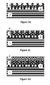
- a Si, sapphire, or SiC substrate (1) is provided.
- a III-V layer (2) is provided, such as a III-V buffer layer.
- the buffer layer may comprise different sub-layers.
- an III-N layer is provided, such as an AlN layer, in order to compensate for difference in lattice dimension of substrate and subsequent applied layers.
- other III-V layers may be provided, such as GaN/AlGaN buffer layers.
- a first epitaxial semiconducting layer (3) such as a III-V layer, wherein preferably a surface orientation of the III-V layer is selected from ⁇ 1 1 01 ⁇ , ⁇ 0002 ⁇ , is provided.
- the layer is an n-type III-V layer, such as an n-type GaN layer.
- the thickness of the layer is from 500 nm - 5 ⁇ m, such as 2-3 ⁇ m.
- a regular pattern of pits is provided by etching the III-V layer, in an example using dry etch.
- the pitch has a width of 1 ⁇ m, a length of 1 ⁇ m, and a depth of 1 ⁇ m.
- a CI-based plasma chemistry can be used in combination with a SiN mask.
- the increased surface area is determined by the aspect ratio 2h/(d1+d2), where h is the trench depth/the pillar height.
- d1 and d2 are the respective feature size of the top and bottom spacing.
- d1, d2 and h are all 1 ⁇ m and as a consequence the surface area relating to the active area is doubled.
- a ⁇ 110> direction of Si(111) substrates is parallel to ⁇ 1120> direction of GaN.
- the most stable facets are ⁇ 1 1 01 ⁇ .
- a thin 100 nm thick intermediate layer (4) is provided, in an example a conformal grown InGaN layer.
- a second epitaxial semiconducting p-type III-V layer (5) is provided, such as p-type III-N.
- p-type GaN is provided, having a thickness from 500 nm - 5 ⁇ m, such as 2-3 ⁇ m.
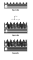
- Figures 3a-3d show cross sections of a device manufactured according to a method of an embodiment of the present invention.
- a Si, sapphire, or SiC substrate (1) is provided.
- a regular pattern of pits is provided by etching the substrate, in an example using dry etch.
- the pitch has a width of 1 ⁇ m, a length of 1 ⁇ m, and a depth of 1 ⁇ m.
- first III-V layer (3) is provided, such as a III-V layer.
- the layer may comprise different sub-layers.
- an III-N layer is provided, such as an GaN layer, wherein preferably a surface orientation of the III-V layer is selected from ⁇ 1 1 01 ⁇ , ⁇ 0002 ⁇ .
- the layer is an n-type III-V layer, such as an n-type GaN layer.
- the thickness of the layer is from 500 nm - 5 ⁇ m, such as 2-3 ⁇ m.
- a thin 100 nm layer (4) is provided, in an example a conformal grown InGaN/GaN layer.
- an p-type III-V layer (5) is provided, such as p-type III-N.
- p-type GaN is proved, having a thickness from 500 nm - 5 ⁇ m, such as 2-3 ⁇ m. As the angle between (1101) and (0002) is 58°, the active area is almost doubled.
- a semi-polar direction has a low internal piezoelectric field, which allows to grow thicker quantum wells (e.g. InGaN wells) because of a less pronounced QCSE (quantum confined stark effect).
- a thick quantum well will reduce the effective carrier density further.
- the patterned structures can be formed on GaN templates or on substrates with specific shape or orientation.
- the increased area is amongst others determined by an aspect ratio of the patterned structures.
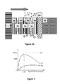
- Figures 4a-4b show schematically in cross sections the band diagrams with the multiple quantum wells with (1) being the substrate+GaN, (3) the n-type MQW, and (5) the p-type GaN of a device manufactured using a method according to an embodiment of the present invention.
- the device may in an example - with respect to substrate (1), first III-V layers (3a, 3b, 3c), and second III-V layers (5a, 5b) - be manufactured in a similar way as the devices shown in figures 2 and 3 , respectively.
- the arrow indicates subsequent layers.
- InGaN/InGaN MQW Another possibility to minimize efficiency droop is to use InGaN/InGaN MQW. Due to a short diffusion length and low mobility of holes in GaN, most of light is emitted in the top single quantum well. It has been found that a GaN barrier in a MQW region is so high that the injected holes are accumulated in e.g. a top InGaN well. By using InGaN/InGaN quantum wells, the barrier height is reduced and holes have more chance to reach bottom InGaN wells. In this way, the total carrier density in the top quantum well is significantly reduced.
- Figure 5 shows internal quantum efficiency versus current density of a prior art device (1), of a prior art device having a low internal quantum efficiency (3) and of the present device (2).
- curve (2) shows internal quantum efficiency versus current density of a prior art device (1), of a prior art device having a low internal quantum efficiency (3) and of the present device (2).
- efficiency droop is also less pronounced but this is less or not disturbing as the absolute quantum efficiency is low.
Landscapes
- Led Devices (AREA)
- Chemical & Material Sciences (AREA)
- Crystallography & Structural Chemistry (AREA)
- Engineering & Computer Science (AREA)
- Materials Engineering (AREA)
- Junction Field-Effect Transistors (AREA)
Applications Claiming Priority (1)
| Application Number | Priority Date | Filing Date | Title |
|---|---|---|---|
| US201161472080P | 2011-04-05 | 2011-04-05 |
Publications (1)
| Publication Number | Publication Date |
|---|---|
| EP2509120A1 true EP2509120A1 (de) | 2012-10-10 |
Family
ID=46149135
Family Applications (1)
| Application Number | Title | Priority Date | Filing Date |
|---|---|---|---|
| EP12162196A Withdrawn EP2509120A1 (de) | 2011-04-05 | 2012-03-29 | Halbleiterbauelement und -verfahren |
Country Status (3)
| Country | Link |
|---|---|
| US (1) | US9196477B2 (de) |
| EP (1) | EP2509120A1 (de) |
| JP (1) | JP2012222354A (de) |
Cited By (1)
| Publication number | Priority date | Publication date | Assignee | Title |
|---|---|---|---|---|
| CN108231908A (zh) * | 2017-11-24 | 2018-06-29 | 西安电子科技大学 | GaN/AlGaN横向超级结二极管及其制作方法 |
Families Citing this family (1)
| Publication number | Priority date | Publication date | Assignee | Title |
|---|---|---|---|---|
| US10374128B2 (en) * | 2013-12-12 | 2019-08-06 | Terahertz Device Corporation | Electrical contacts to light-emitting diodes for improved current spreading and injection |
Citations (7)
| Publication number | Priority date | Publication date | Assignee | Title |
|---|---|---|---|---|
| EP1667241A1 (de) * | 2003-08-19 | 2006-06-07 | Nichia Corporation | Halbleiterbauelement |
| WO2007098215A2 (en) * | 2006-02-17 | 2007-08-30 | The Regents Of The University Of California | Method for growth of semipolar (al,in,ga,b)n optoelectronic devices |
| EP1901357A2 (de) * | 2006-09-15 | 2008-03-19 | Osram Opto Semiconductors GmbH & Co. OHG | Optoelektronischer Halbleiterchip |
| WO2009111790A1 (en) | 2008-03-07 | 2009-09-11 | Trustees Of Boston University | Optical devices featuring nonpolar textured semiconductor layers |
| US20100006878A1 (en) | 2008-07-08 | 2010-01-14 | Samsung Electro-Mechanics Co., | Semiconductor light emitting device having patterned substrate and manufacturing method of the same |
| US20100155704A1 (en) | 2008-12-23 | 2010-06-24 | Jeong Tak Oh | Nitride semiconductor light emitting device and method of manufacturing the same |
| US20100264454A1 (en) | 2006-12-22 | 2010-10-21 | Koninklijke Philips Electronics N.V. | Semiconductor light emitting device growing active layer on textured surface |
Family Cites Families (22)
| Publication number | Priority date | Publication date | Assignee | Title |
|---|---|---|---|---|
| JP2515051B2 (ja) * | 1990-11-14 | 1996-07-10 | 三菱電機株式会社 | 半導体光素子及びその製造方法 |
| JPH0529714A (ja) * | 1991-07-24 | 1993-02-05 | Mitsubishi Electric Corp | 量子細線または量子箱 |
| JP4595198B2 (ja) * | 2000-12-15 | 2010-12-08 | ソニー株式会社 | 半導体発光素子及び半導体発光素子の製造方法 |
| JP3536978B2 (ja) * | 2000-12-27 | 2004-06-14 | 独立行政法人産業技術総合研究所 | 量子細線または量子井戸層の形成方法、及び該形成方法により形成された量子細線または量子井戸層を用いた分布帰還半導体レーザ |
| JP4055503B2 (ja) * | 2001-07-24 | 2008-03-05 | 日亜化学工業株式会社 | 半導体発光素子 |
| EP1291904A3 (de) * | 2001-09-10 | 2009-10-07 | FUJIFILM Corporation | GaN-Substrat, das auf einer feinen diskreten Löcher aufweisenden GaN-Schicht gebildet wurde, die durch selektives Wachstum hergestellt worden ist |
| JP3854560B2 (ja) * | 2002-09-19 | 2006-12-06 | 富士通株式会社 | 量子光半導体装置 |
| JP4304339B2 (ja) * | 2004-01-13 | 2009-07-29 | 独立行政法人産業技術総合研究所 | 量子細線電界効果トランジスタ |
| JP2006165051A (ja) * | 2004-12-02 | 2006-06-22 | Sumitomo Electric Ind Ltd | 半導体発光素子及びその製造方法 |
| JP2007073675A (ja) * | 2005-09-06 | 2007-03-22 | Nippon Telegr & Teleph Corp <Ntt> | 細線構造及び配線並びにその作製方法 |
| US7982205B2 (en) | 2006-01-12 | 2011-07-19 | National Institute Of Advanced Industrial Science And Technology | III-V group compound semiconductor light-emitting diode |
| JP4908886B2 (ja) * | 2006-03-23 | 2012-04-04 | 日本電信電話株式会社 | 半導体装置 |
| JP2008226868A (ja) * | 2007-03-08 | 2008-09-25 | Showa Denko Kk | Iii族窒化物化合物半導体積層構造体 |
| JP5466505B2 (ja) * | 2007-06-27 | 2014-04-09 | ルネサスエレクトロニクス株式会社 | 電界効果トランジスタ、ならびに、該電界効果トランジスタの作製に供される多層エピタキシャル膜 |
| JP2009059851A (ja) | 2007-08-31 | 2009-03-19 | National Institute Of Advanced Industrial & Technology | 半導体発光ダイオード |
| JP2009231561A (ja) * | 2008-03-24 | 2009-10-08 | Nippon Telegr & Teleph Corp <Ntt> | 窒化物半導体結晶薄膜およびその作製方法、半導体装置およびその製造方法 |
| JP5292895B2 (ja) * | 2008-03-31 | 2013-09-18 | 日本電気株式会社 | 窒化物半導体トランジスタ |
| KR101092079B1 (ko) * | 2008-04-24 | 2011-12-12 | 엘지이노텍 주식회사 | 반도체 발광소자 및 그 제조방법 |
| JP2009295753A (ja) * | 2008-06-04 | 2009-12-17 | Showa Denko Kk | Iii族窒化物半導体発光素子の製造方法及びiii族窒化物半導体発光素子、並びにランプ |
| JP5468761B2 (ja) * | 2008-09-25 | 2014-04-09 | 古河電気工業株式会社 | 半導体装置、ウエハ構造体および半導体装置の製造方法 |
| KR101009651B1 (ko) | 2008-10-15 | 2011-01-19 | 박은현 | 3족 질화물 반도체 발광소자 |
| TWI394873B (zh) * | 2009-04-27 | 2013-05-01 | 和椿科技股份有限公司 | 具有週期結構之藍寶石基板之製造方法 |
-
2012
- 2012-03-29 EP EP12162196A patent/EP2509120A1/de not_active Withdrawn
- 2012-04-03 US US13/438,718 patent/US9196477B2/en active Active
- 2012-04-03 JP JP2012084779A patent/JP2012222354A/ja active Pending
Patent Citations (7)
| Publication number | Priority date | Publication date | Assignee | Title |
|---|---|---|---|---|
| EP1667241A1 (de) * | 2003-08-19 | 2006-06-07 | Nichia Corporation | Halbleiterbauelement |
| WO2007098215A2 (en) * | 2006-02-17 | 2007-08-30 | The Regents Of The University Of California | Method for growth of semipolar (al,in,ga,b)n optoelectronic devices |
| EP1901357A2 (de) * | 2006-09-15 | 2008-03-19 | Osram Opto Semiconductors GmbH & Co. OHG | Optoelektronischer Halbleiterchip |
| US20100264454A1 (en) | 2006-12-22 | 2010-10-21 | Koninklijke Philips Electronics N.V. | Semiconductor light emitting device growing active layer on textured surface |
| WO2009111790A1 (en) | 2008-03-07 | 2009-09-11 | Trustees Of Boston University | Optical devices featuring nonpolar textured semiconductor layers |
| US20100006878A1 (en) | 2008-07-08 | 2010-01-14 | Samsung Electro-Mechanics Co., | Semiconductor light emitting device having patterned substrate and manufacturing method of the same |
| US20100155704A1 (en) | 2008-12-23 | 2010-06-24 | Jeong Tak Oh | Nitride semiconductor light emitting device and method of manufacturing the same |
Non-Patent Citations (1)
| Title |
|---|
| WANG C H ET AL: "Internal quantum efficiency measurement in InGaN/GaN UV LEDs with patterned sapphire substrate by photoluminescence and electroluminescence method", CONFERENCE ON LASERS AND ELECTRO-OPTICS (CLEO) AND QUANTUM ELECTRONICS AND LASER SCIENCE CONFERENCE (QELS), 2010 : 16 - 21 MAY 2010, SAN JOSE, CA, USA, IEEE, PISCATAWAY, NJ , USA, 16 May 2010 (2010-05-16), pages 1 - 2, XP031700689, ISBN: 978-1-55752-890-2 * |
Cited By (1)
| Publication number | Priority date | Publication date | Assignee | Title |
|---|---|---|---|---|
| CN108231908A (zh) * | 2017-11-24 | 2018-06-29 | 西安电子科技大学 | GaN/AlGaN横向超级结二极管及其制作方法 |
Also Published As
| Publication number | Publication date |
|---|---|
| US20130001507A1 (en) | 2013-01-03 |
| US9196477B2 (en) | 2015-11-24 |
| JP2012222354A (ja) | 2012-11-12 |
Similar Documents
| Publication | Publication Date | Title |
|---|---|---|
| KR101710159B1 (ko) | Ⅲ족 질화물 나노로드 발광소자 및 그 제조 방법 | |
| US8278125B2 (en) | Group-III nitride epitaxial layer on silicon substrate | |
| US10665748B2 (en) | Light emitting diode and fabrication method therof | |
| KR101622308B1 (ko) | 발광소자 및 그 제조방법 | |
| US20080073655A1 (en) | Optoelectronic semiconductor chip | |
| EP2636078A1 (de) | Festkörper-beleuchtungsvorrichtungen auf der basis von kristallografisch entspannten strukturen | |
| CN101069290A (zh) | 氮化物半导体发光器件及其制造方法 | |
| CN103325904B (zh) | 包括氮化物基半导体全方向反射器的发光装置 | |
| US10090437B2 (en) | LED having etched light emitting surface for increased light extraction | |
| KR20120083084A (ko) | 나노 로드 발광 소자 및 그 제조 방법 | |
| JP2023541295A (ja) | 単一ウエハ上に集積された三色光源 | |
| CN106601885A (zh) | 一种发光二极管的外延结构及其生长方法 | |
| KR20130061182A (ko) | 반도체 층 시퀀스의 제조 방법, 복사 방출 반도체 칩, 및 광전 소자 | |
| US9202967B2 (en) | Method for producing a thin-film semiconductor body and thin-film semiconductor body | |
| TWI493747B (zh) | 發光二極體及其形成方法 | |
| KR100682873B1 (ko) | 반도체 발광 소자 및 그 제조 방법 | |
| CN105762241A (zh) | 一种增强注入型的发光二极管的外延结构制作方法 | |
| KR20090089975A (ko) | 반도체 발광소자 및 그 제조방법 | |
| US9196477B2 (en) | Semiconductor device and method | |
| KR102059133B1 (ko) | GaN 베이스 발광소자와 기계적 후처리를 이용한 그 제조방법 | |
| CN110534624B (zh) | 用于生长半导体超薄外延结构的一种外延层 | |
| KR100812738B1 (ko) | 표면 요철 형성방법 및 그를 이용한 질화물계 반도체발광소자의 제조방법 | |
| KR20140071161A (ko) | 결정방향 정합성을 나타내는 패턴이 형성된 기판을 포함하는 반도체 발광소자 및 이의 제조방법 | |
| US6875995B2 (en) | Heterogeneous bandgap structures for semiconductor devices and manufacturing methods therefor | |
| KR102192086B1 (ko) | 질화물 양자점을 갖는 소자 및 그 제조방법 |
Legal Events
| Date | Code | Title | Description |
|---|---|---|---|
| PUAI | Public reference made under article 153(3) epc to a published international application that has entered the european phase |
Free format text: ORIGINAL CODE: 0009012 |
|
| AK | Designated contracting states |
Kind code of ref document: A1 Designated state(s): AL AT BE BG CH CY CZ DE DK EE ES FI FR GB GR HR HU IE IS IT LI LT LU LV MC MK MT NL NO PL PT RO RS SE SI SK SM TR |
|
| AX | Request for extension of the european patent |
Extension state: BA ME |
|
| STAA | Information on the status of an ep patent application or granted ep patent |
Free format text: STATUS: THE APPLICATION IS DEEMED TO BE WITHDRAWN |
|
| 18D | Application deemed to be withdrawn |
Effective date: 20130411 |