EP2509209A2 - Redresseur actif avec un équilibrage de tension des condensateurs de sortie - Google Patents
Redresseur actif avec un équilibrage de tension des condensateurs de sortie Download PDFInfo
- Publication number
- EP2509209A2 EP2509209A2 EP12162891A EP12162891A EP2509209A2 EP 2509209 A2 EP2509209 A2 EP 2509209A2 EP 12162891 A EP12162891 A EP 12162891A EP 12162891 A EP12162891 A EP 12162891A EP 2509209 A2 EP2509209 A2 EP 2509209A2
- Authority
- EP
- European Patent Office
- Prior art keywords
- output
- output capacitor
- adjustment value
- voltage
- accumulated
- Prior art date
- Legal status (The legal status is an assumption and is not a legal conclusion. Google has not performed a legal analysis and makes no representation as to the accuracy of the status listed.)
- Withdrawn
Links
- 239000003990 capacitor Substances 0.000 title claims abstract description 101
- 230000001105 regulatory effect Effects 0.000 claims abstract description 9
- 230000004044 response Effects 0.000 claims abstract description 3
- 238000000034 method Methods 0.000 claims description 10
- 238000012544 monitoring process Methods 0.000 claims 1
- 230000009466 transformation Effects 0.000 description 10
- 238000010586 diagram Methods 0.000 description 6
- 230000003247 decreasing effect Effects 0.000 description 5
- 238000004364 calculation method Methods 0.000 description 4
- 230000000694 effects Effects 0.000 description 3
- 238000000844 transformation Methods 0.000 description 3
- 238000012937 correction Methods 0.000 description 2
- 230000004048 modification Effects 0.000 description 2
- 238000012986 modification Methods 0.000 description 2
- 238000012545 processing Methods 0.000 description 2
- 230000004075 alteration Effects 0.000 description 1
- 230000008901 benefit Effects 0.000 description 1
- 230000008859 change Effects 0.000 description 1
- 238000004891 communication Methods 0.000 description 1
- 230000001934 delay Effects 0.000 description 1
- 238000013461 design Methods 0.000 description 1
- 238000001914 filtration Methods 0.000 description 1
- 238000005070 sampling Methods 0.000 description 1
- 238000006467 substitution reaction Methods 0.000 description 1
Images


Classifications
-
- H—ELECTRICITY
- H02—GENERATION; CONVERSION OR DISTRIBUTION OF ELECTRIC POWER
- H02M—APPARATUS FOR CONVERSION BETWEEN AC AND AC, BETWEEN AC AND DC, OR BETWEEN DC AND DC, AND FOR USE WITH MAINS OR SIMILAR POWER SUPPLY SYSTEMS; CONVERSION OF DC OR AC INPUT POWER INTO SURGE OUTPUT POWER; CONTROL OR REGULATION THEREOF
- H02M7/00—Conversion of AC power input into DC power output; Conversion of DC power input into AC power output
- H02M7/02—Conversion of AC power input into DC power output without possibility of reversal
- H02M7/04—Conversion of AC power input into DC power output without possibility of reversal by static converters
- H02M7/06—Conversion of AC power input into DC power output without possibility of reversal by static converters using discharge tubes without control electrode or semiconductor devices without control electrode
- H02M7/066—Conversion of AC power input into DC power output without possibility of reversal by static converters using discharge tubes without control electrode or semiconductor devices without control electrode particular circuits having a special characteristic
-
- H—ELECTRICITY
- H02—GENERATION; CONVERSION OR DISTRIBUTION OF ELECTRIC POWER
- H02M—APPARATUS FOR CONVERSION BETWEEN AC AND AC, BETWEEN AC AND DC, OR BETWEEN DC AND DC, AND FOR USE WITH MAINS OR SIMILAR POWER SUPPLY SYSTEMS; CONVERSION OF DC OR AC INPUT POWER INTO SURGE OUTPUT POWER; CONTROL OR REGULATION THEREOF
- H02M7/00—Conversion of AC power input into DC power output; Conversion of DC power input into AC power output
- H02M7/02—Conversion of AC power input into DC power output without possibility of reversal
- H02M7/04—Conversion of AC power input into DC power output without possibility of reversal by static converters
- H02M7/12—Conversion of AC power input into DC power output without possibility of reversal by static converters using discharge tubes with control electrode or semiconductor devices with control electrode
- H02M7/21—Conversion of AC power input into DC power output without possibility of reversal by static converters using discharge tubes with control electrode or semiconductor devices with control electrode using devices of a triode or transistor type requiring continuous application of a control signal
- H02M7/217—Conversion of AC power input into DC power output without possibility of reversal by static converters using discharge tubes with control electrode or semiconductor devices with control electrode using devices of a triode or transistor type requiring continuous application of a control signal using semiconductor devices only
- H02M7/219—Conversion of AC power input into DC power output without possibility of reversal by static converters using discharge tubes with control electrode or semiconductor devices with control electrode using devices of a triode or transistor type requiring continuous application of a control signal using semiconductor devices only in a bridge configuration
-
- H—ELECTRICITY
- H02—GENERATION; CONVERSION OR DISTRIBUTION OF ELECTRIC POWER
- H02M—APPARATUS FOR CONVERSION BETWEEN AC AND AC, BETWEEN AC AND DC, OR BETWEEN DC AND DC, AND FOR USE WITH MAINS OR SIMILAR POWER SUPPLY SYSTEMS; CONVERSION OF DC OR AC INPUT POWER INTO SURGE OUTPUT POWER; CONTROL OR REGULATION THEREOF
- H02M1/00—Details of apparatus for conversion
- H02M1/0003—Details of control, feedback or regulation circuits
- H02M1/0012—Control circuits using digital or numerical techniques
-
- H—ELECTRICITY
- H02—GENERATION; CONVERSION OR DISTRIBUTION OF ELECTRIC POWER
- H02M—APPARATUS FOR CONVERSION BETWEEN AC AND AC, BETWEEN AC AND DC, OR BETWEEN DC AND DC, AND FOR USE WITH MAINS OR SIMILAR POWER SUPPLY SYSTEMS; CONVERSION OF DC OR AC INPUT POWER INTO SURGE OUTPUT POWER; CONTROL OR REGULATION THEREOF
- H02M1/00—Details of apparatus for conversion
- H02M1/42—Circuits or arrangements for compensating for or adjusting power factor in converters or inverters
- H02M1/4208—Arrangements for improving power factor of AC input
- H02M1/4216—Arrangements for improving power factor of AC input operating from a three-phase input voltage
-
- Y—GENERAL TAGGING OF NEW TECHNOLOGICAL DEVELOPMENTS; GENERAL TAGGING OF CROSS-SECTIONAL TECHNOLOGIES SPANNING OVER SEVERAL SECTIONS OF THE IPC; TECHNICAL SUBJECTS COVERED BY FORMER USPC CROSS-REFERENCE ART COLLECTIONS [XRACs] AND DIGESTS
- Y02—TECHNOLOGIES OR APPLICATIONS FOR MITIGATION OR ADAPTATION AGAINST CLIMATE CHANGE
- Y02B—CLIMATE CHANGE MITIGATION TECHNOLOGIES RELATED TO BUILDINGS, e.g. HOUSING, HOUSE APPLIANCES OR RELATED END-USER APPLICATIONS
- Y02B70/00—Technologies for an efficient end-user side electric power management and consumption
- Y02B70/10—Technologies improving the efficiency by using switched-mode power supplies [SMPS], i.e. efficient power electronics conversion e.g. power factor correction or reduction of losses in power supplies or efficient standby modes
Definitions
- the present invention relates generally to active rectifier, and in particular to control schemes for active rectifiers.
- Active rectifiers which replace passive diode components with actively controlled switching elements (such as MOSFETs) provide improved efficiency and power factor correction, thereby reducing the overall weight of the rectification system.
- Various active rectifier topologies and control schemes have been designed to further improve the efficiency and power factor correction provided by active rectification.
- An active rectification system includes an active rectifier that converts an alternating current (AC) input to a direct current (DC) output.
- the active rectifier includes a plurality of switching devices and at least a first output capacitor and a second output capacitor connected at the DC output of the active rectifier.
- the system further includes a controller having a DOC output regulation portion and an output capacitor balancing portion.
- the DOC output regulation portion monitors the DC output and in response generates control signals for regulating the DC output to a desired value.
- the output capacitor balancing portion monitors first and second output capacitor voltages associated with the first and second output capacitors, respectively, and generates an accumulated adjustment value that modifies the control signals provided by the DC output regulation portion to balance the first and second output capacitor voltages.
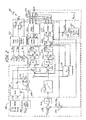
- FIG. 1 is a circuit diagram of an active rectification system according to an embodiment of the present invention.
- FIG. 2 is a block diagram illustrating a rectifier control algorithm according to an embodiment of the present invention.
- FIG. 3 is a block diagram illustrating calculation of the small increment adjustments according to an embodiment of the present invention.
- a multi-level active rectifier converts an alternating current (AC) input to a direct current (DC) output and includes at least first and second output capacitors connected at the output of the active rectifier.
- a controller regulates the operation of the active rectifier, including regulating the DC output of the active rectifier to a desired value and balancing voltages provided across the first and second output capacitors.
- FIG. 1 is a circuit diagram of an active rectification system according to an embodiment of the present invention, where Vsa, Vsb, Vsc represent a source input three-phase voltage, and Vpa, Vpb, Vpc represent a three-phase pole voltage.
- An active rectifier 102 which includes a plurality of active switching devices S 1 , S 2 , S 3 , converts the input three-phase voltage Vsa, Vsb, Vsc to a DC output Vdc.
- a controller 101 may be a computer processor or processing apparatus configured and disposed to regulate the DC output Vdc to a desired value through selective control of the active switching devices S 1 , S 2 , S 3 . In particular, controller 101 monitors the output capacitor voltages Vdc1, Vdc2 and acts to balance the voltage across both capacitors while maintaining a desired DC output voltage Vdc.
- the active rectifier 102 is a three-phase three-level switching rectifier that may be realized using a VIENNA rectifier.
- VIENNA rectifier any other VIENNA rectifier topology as well as any suitable multi-level active rectifier may be used according to any desired implementation.
- the active rectifier 102 may include at least three switches S 1 , S 2 , and S 3 .
- Each of the switches S 1 , S 2 , and S 3 is surrounded by balanced diode bridges 111, 112, and 113, respectfully.
- the first diode bridge 111 may be coupled between a first diode D 1 and a second diode D 2 .
- the second diode bridge 112 may be coupled between a third diode D 3 and a fourth diode D 4 .
- the third diode bridge may be coupled between a fifth diode D 5 and a sixth diode D 6 .
- each of the three switches S 1 , S 2 , and S 3 may be configured to switch between at least two states.
- the at least two states may include an open state, and a closed state.
- the open and closed states as controlled using controller 101, realize three-level switching and active rectification using two level switches with two states.
- the active rectifier 102 may further include a first capacitance C 1 coupled across each of the first, third, and fifth diodes D 1 , D 3 , and D 5 , and a center point of each diode bridge 111, 112, and 113, respectfully.
- the active rectifier 102 may further include a second capacitance C 2 coupled across each of the second, fourth, and fifth diodes D 2 , D 4 , and D 6 , and a center point of each diode bridge 111, 112, and 113, respectfully.
- the system 100 may include a load and/or load resistance R L , coupled in parallel across both the first and second capacitances C 1 and C 2 of active rectifier 102.
- the system 100 may further include boost inductors L a , L b , and L c ; each corresponding to a single phase of three-phase AC input current/power source ( Vs a , Vs b , and Vs c ).
- the controller 101 is in electrical communication with each of the switches S 1 , S 2 , and S 3 .
- the controller 101 may direct each of the switches S 1 , S 2 , and S 3 to change between one of the open and closed states available to the switches S 1 , S 2 , and S 3 , based upon a control scheme that regulates the DC output voltage Vdc to a desired value, and in addition balances the respective output capacitor voltages Vdc 1 , Vdc 2 provided across capacitors C 1 and C 2 , respectively.
- FIG. 2 is a block diagram illustrating a rectifier control algorithm executed by controller 101 according to an embodiment of the present invention.
- the control methodology may be implemented as computer executable instructions that, when executed on any suitable processor, direct the processor to perform and execute the methodology as described below.
- the control methodology is divided, for purposes of this description, into a DC output regulation portion 200 responsible for generating control signals for regulating the DC output of the active rectifier 102 (shown in FIG. 1 ) and an output capacitor balancing portion 228 that modifies the control signals provided by the DC output regulation portion 200 to balance output capacitor voltages Vdc 1 , Vdc 2 across capacitors C 1 and C 2 , respectively.
- a DC output regulation portion 200 responsible for generating control signals for regulating the DC output of the active rectifier 102 (shown in FIG. 1 )
- an output capacitor balancing portion 228 that modifies the control signals provided by the DC output regulation portion 200 to balance output capacitor voltages Vdc 1 , Vdc 2 across capacitors C 1 and C 2 ,
- the control signals provided by DC output regulation portion 200 are desired pole voltage values Vp a , VP b , Vp c , which are modified by an accumulated adjustment value Vadj_sum generated by the output capacitor balancing portion 228.
- the control signals provided by DC output regulation portion 200 represent the control signals required to regulate the DC output Vdc to a desired value, while the accumulated adjustment value Vadj_sum represents the modification required to balance output capacitor voltages Vdc 1 , Vdc 2 .
- the three phase current input i a , i b , i c , voltage input Vs a as well as the two capacitor voltage outputs Vdc 1 , Vdc 2 are continuously monitored by controller 101 (shown in FIG. 1 ).
- the two output DC capacitor voltages Vdc 1 , Vdc 2 are summed to provide a value representative of the DC output voltage Vdc.
- the resulting sum is subtracted from the desired output DC voltage Vdc ref at block 205.
- the resulting difference between the monitored DC output voltage Vdc and the desired DC output voltage Vdc ref is then processed through a proportional and integral control at block 204 and then limited at block 210.
- the output of block 210 is the d -component reference of the current.
- Block 202 of Fig. 2 is the phase and frequency detector.
- Phase A of the input 3-phase voltage is used here to detect the phase angle and frequency of the input voltage.
- the current three-phase inputs i a , i b , i c of active rectifier 102 are transformed using Clarke transformations.
- Clarke transformations One example of a Clarke transformation is depicted in Equations 1 and 2, below. However, it should be noted that any suitable implementation including different equations may also be applicable.
- the outputs i ⁇ , i ⁇ of the Clarke transformations are input to block 207, where the Clarke outputs are transformed into a d-q frame through Park transformations using the detected phase angle ⁇ .
- a Park transformation is depicted in Equations 3 and 4, below. However, it should be noted that any suitable implementation including different equations may also be applicable.
- the angular frequency ⁇ is multiplied by the single phase boost inductance L at block 208.
- the resulting ⁇ L is then multiplied by the d-q components i d , i q of the current at blocks 211 and 212.
- d-q current components i d , i q of the measured current are subtracted from the d-q reference component i dref , i qref of the current at blocks 213 and 214.
- Proportional and integral (PI) control of the difference outputs at blocks 213 and 214 is performed at blocks 216 and 217, respectively.
- a suitable proportional Laplace transform for blocks 216 and 217 is depicted in Equation 5, below: K p + K i s In Equation 5, Kp is proportional gain and K i is integral gain.
- Block 218 subtracts the output of block 216 and the multiplication of ⁇ L and I d performed at block 212 from zero (which is the expected q-component of the input voltage).
- Block 219 subtracts the output of block 217, adds the multiplication of ⁇ L and I q performed at block 211, and adds the maximum expected value of the d -component of the input voltage (Max vsd ).
- the outputs of blocks 218 and 219 are then limited using voltage limiters 220 and 221, respectively.
- the outputs of blocks 220 and 221 are the d-q components of the resulting pole voltage Vp q , Vp d .
- the d-q components of the resulting pole voltages Vp q , Vp d are then transformed at blocks 224 and 225 using an inverse Park transformation, inverse Clark transformation, and the phase angle ⁇ or a modified ⁇ that includes delays due to hardware implementation artifacts of the control algorithm to the 3-phase components of the resulting pole voltage.
- Equation 6 cos ⁇ ⁇ Vp d - sin ⁇ ⁇ Vp q
- Vp ⁇ sin ⁇ ⁇ Vp d + cos ⁇ ⁇ Vp q
- Vp d The d-q components of the resulting pole voltages Vp q , Vp d (outputs of blocks 220 and 221) along with the calculated reference d -component of the current i dref (output of block 210) are used in block 215 to calculate the reference q -component of the current.
- Block 215 performs a phase alignment of the input current to the resulting pole voltage of the active rectifier. This is done by calculating the q -component current reference such that the input current and the pole voltage are in phase alignment.
- the calculated q -component current reference is to be used as a reference during the subsequent control loop processing (i.e., the following instance the control loop is processed).
- the reference q-component i qref is set equal to zero in order to achieve a power factor of one.
- the reference q-component i qref may also be set or calculated to a desired value to achieve a desired result (e.g., calculating the reference q-component i qref to align the three-phase input voltage with the three-phase output voltage).
- the pole voltages Vp a , Vp b , and Vp c provided as a result of the inverse Clarke transformation represent the pole voltages required to generate the desired DC output voltage, without concern for the capacitor voltage outputs Vdc1, Vdc2.
- An adjustment signal V adj is summed with the pole voltages Vp a , Vp b , and Vp c at blocks 234, 235 and 236, respectively, for provision to block 223 for calculation of pulse width modulation (PWM) signals.
- PWM signals are provided to gate drive 222, which selectively controls the open/close state of the plurality of switches included within active rectifier 102. In this way, the control methodology provided with respect to FIG.
- control signals e.g., desired pole voltages Vp a , Vp b , Vp c . It should be understood that other well-known control algorithms may be employed to regulate the output voltage of an active rectifier, and may be used in conjunction with the output capacitor balancing portion 228.
- the output capacitor balancing portion 228 generates an accumulated adjustment value that is provided to modify the control signals generated by DC output regulation portion 200 in order to balance the output capacitor voltages Vdc1, Vdc2.
- the output capacitor balancing portion 228 includes difference calculator block 230, small increment capacitor voltage balancing block 232, and difference blocks 234, 235 and 236.
- Output capacitor balancing portion 228 acts to balance the capacitor voltage outputs Vdc 1 , Vdc 2 without affecting the sum of capacitor voltage outputs (i.e., DC output Vdc, which should remain equal to the desired DC output value).
- the first output capacitor C 1 is charged by positive phase voltages, while the second output capacitor C 2 is charged by negative phase voltages.
- Increasing the pole voltages has the effect of increasing the voltage on the first output capacitor C 1 relative to the second output capacitor C 2
- decreasing the pole voltages has the effect of increasing the voltage on the second output capacitor C 2 relative to the first output capacitor C 1 .
- the opposite configuration may be true.
- a difference signal Vdc diff is calculated by subtracting the second capacitor output voltage Vdc 2 from the first capacitor output voltage Vdc 1 at difference calculator block 230.
- a non-zero value represents an imbalance in the capacitor output voltages Vdc 1 , Vdc 2 .
- the calculated difference signal Vdc diff is provided to small increment capacitor voltage balancing block 232, which calculates an accumulated adjustment value Vadj_sum to be subtracted from the pole voltages Vp a , Vp b , and Vp c .
- PWM calculator block 223 which supplies the PWM signals to gate driver block 222 based on the pole voltages Vp a , Vp b , Vp c as adjusted by the accumulated adjustment value Vadj_sum.
- gate driver block 222 drives the plurality of switches included within three-level rectifier 102.
- the adjustment value is provided directly to PWM calculator 223 for use in calculating the PWM signals to be provided to active rectifier 102.
- Block 223 or the combination of blocks 222 and 223 may also be referred to as a PWM controller.
- FIG. 3 is a block diagram of small increment capacitor voltage balancing block 232 illustrating the calculation of the small increment adjustments according to an embodiment of the present invention.
- the calculated difference signal Vdc diff is provided as an input to m -moving average filter 302, which filters the calculated difference signal to smooth out short-term variations or transients.
- Successive samples of the difference signal Vdc diff are stored in memory cells 310, 314,... 318, respectively.
- Blocks 312, 316, ... 320 sum the values stored in each of the memory cells to provide an accumulated sum of the difference signals Vdc diff over a number m of samples.
- the accumulated sum is divided by the number of samples m at block 322 to provide an m -moving average Vdc diff_ave of the calculated difference signal Vdc diff .
- the m -moving average Vdc diff_ave provided by block 302 is one example of time-averaged filtering that may be employed to smooth the calculated difference signal Vdc diff and reduce the effect of transients on the accumulated adjustment value Vadj_sum. In other embodiments, other types of filters may be employed depending on the application.
- the sample size of the m -moving average filter is selected based on the number of samples collected during one cycle of the three-phase input voltage. For example, in the frequency of the three-phase input voltage is approximately 400 Hz, and the sampling frequency is approximately 50 kHz, then the sample size m would be equal to approximately 125.
- Adjustment calculator 304 calculates an adjustment value based on the calculated difference between the first output capacitor voltage and the second output capacitor voltage as provided by the m -moving filter 302 (i.e., determines whether or not to modify the accumulated adjustment value Vadj_sum ). Adjustment calculator 304 indicates visually the criteria used to select the increment value. If the average difference signal Vdc diff_avg is greater than a positive threshold value Vthreshold, then a positive increment is selected for addition to the accumulated adjustment value Vadj_sum by accumulator 305.
- Vthreshold If the average difference signal Vdc diff_avg is less than a negative threshold value Vthreshold, then a negative increment is selected for addition to the accumulated adjustment value Vadj_sum by accumulator 305 (i.e., an increment value is subtracted from the accumulated adjustment value). If the average difference value Vdc diff_avg is between the positive threshold value and the negative threshold value, then no increment value is provided for addition/subtraction.
- the magnitude of the increment value V adj is selected to maintain the adjustment sum value fixed as much as possible, while balancing the capacitor output voltages in a timely fashion.
- the smaller the value of the increment value V adj the longer it will take to balance the capacitor output voltages.
- the larger the increment value V adj the greater fluctuations in the accumulated adjustment value V adj_sum .
- a plurality of increment values may be provided of varying magnitudes with respect to different threshold values (i.e., increasing increment values with increasing threshold values).
- the accumulator 305 accumulates calculated adjustment values to generate an accumulated adjustment value Vadj_sum.
- the accumulator 305 includes a summer block 306 and a memory cell 308.
- Memory cell 308 stores the accumulated adjustment value Vadj_sum, which is continuously modified by subsequent calculations of increment values Vadj.
- Summer block 306 adds the stored adjustment sum value to the small increment value provided by adjustment block 304 to generate an accumulated adjustment value Vadj_sum.
- imbalances detected by the comparison of capacitor output voltages Vdc 1 , Vdc 2 as represented by a difference signal Vdc diff is used as feedback to modify the control signal outputs (i.e., in this case, calculated pole voltages Vp a , Vp b , Vp c ) to balance the output capacitor voltages Vdc 1 , Vdc 2 .
- the adjustment calculator 304 selects an adjustment value Vadj based on calculated average difference signal Vdc diff_avg and the accumulator block 305 accumulates the selected adjustment values to generate an accumulated adjustment value Vadj_sum, which is combined with the control signals generated by the DC output regulation portion 200 (shown in FIG. 2 ) to balance the output capacitor voltages Vdc 1 , Vdc 2 .
- a benefit of balancing the capacitor output voltages Vdc 1 , Vdc 2 is that equal loading and stress is provided across capacitors C 1 and C 2 .
- balancing of the capacitor output voltages using the small increment capacitor voltage algorithm reduces the 4 th harmonic components of the input 3-phase AC currents which may be desired when designing the active rectifier.
Landscapes
- Engineering & Computer Science (AREA)
- Power Engineering (AREA)
- Rectifiers (AREA)
Applications Claiming Priority (1)
| Application Number | Priority Date | Filing Date | Title |
|---|---|---|---|
| US13/079,925 US8437158B2 (en) | 2011-04-05 | 2011-04-05 | Active rectification output capacitors balancing algorithm |
Publications (2)
| Publication Number | Publication Date |
|---|---|
| EP2509209A2 true EP2509209A2 (fr) | 2012-10-10 |
| EP2509209A3 EP2509209A3 (fr) | 2015-09-30 |
Family
ID=45999637
Family Applications (1)
| Application Number | Title | Priority Date | Filing Date |
|---|---|---|---|
| EP12162891.1A Withdrawn EP2509209A3 (fr) | 2011-04-05 | 2012-04-02 | Redresseur actif avec un équilibrage de tension des condensateurs de sortie |
Country Status (2)
| Country | Link |
|---|---|
| US (1) | US8437158B2 (fr) |
| EP (1) | EP2509209A3 (fr) |
Cited By (5)
| Publication number | Priority date | Publication date | Assignee | Title |
|---|---|---|---|---|
| CN102801348A (zh) * | 2012-06-11 | 2012-11-28 | 上海电机学院 | 三相五电平逆变器 |
| EP2814154A1 (fr) * | 2013-06-14 | 2014-12-17 | Hamilton Sundstrand Corporation | Procédé de réduction de la distorsion de courant d'entrée dans un redresseur |
| EP2940481A1 (fr) * | 2014-04-29 | 2015-11-04 | LSIS Co., Ltd. | Système de surveillance de puissance instantanée pour système hvdc |
| EP2953252A3 (fr) * | 2014-06-05 | 2016-04-27 | Hamilton Sundstrand Corporation | Systèmes et procédés pour contrôler des redresseurs actifs |
| CN106257816A (zh) * | 2015-06-19 | 2016-12-28 | 整流器技术太平洋有限公司 | 包括三个单相模块的三相交流到直流电力转换器的控制 |
Families Citing this family (9)
| Publication number | Priority date | Publication date | Assignee | Title |
|---|---|---|---|---|
| US20140119074A1 (en) * | 2012-10-31 | 2014-05-01 | Christopher J. Courtney | Operation of multichannel active rectifier |
| US9190929B2 (en) * | 2013-02-27 | 2015-11-17 | Varentec, Inc. | Multi-level rectifiers |
| CN103944167B (zh) * | 2014-04-04 | 2016-04-20 | 武汉武新电气科技有限公司 | 一种平衡电容电压的方法和装置 |
| US10042007B2 (en) | 2015-02-04 | 2018-08-07 | Liebert Corporation | Method for detecting a failing rectifier or rectifier source |
| DK3068024T3 (en) * | 2015-03-09 | 2018-04-23 | Siemens Ag | Procedure for controlling a Vienna rectifier |
| FR3082678B1 (fr) * | 2018-06-15 | 2020-05-22 | Renault S.A.S | Procede de commande d'un redresseur de vienne. |
| CN109494995B (zh) * | 2018-10-25 | 2020-08-28 | 江苏大学 | 一种适用于vienna整流器的中点电位平衡控制方法 |
| IT202100002243A1 (it) * | 2021-02-02 | 2022-08-02 | Eldor Corp Spa | Dispositivo correttore del fattore di potenza ed apparato per la conversione di una corrente alternata trifase in una corrente continua |
| CN115250059B (zh) * | 2021-04-26 | 2025-08-22 | 佛山市顺德区美的电子科技有限公司 | 一种电压控制方法、装置、家电设备及计算机存储介质 |
Family Cites Families (9)
| Publication number | Priority date | Publication date | Assignee | Title |
|---|---|---|---|---|
| JP3221828B2 (ja) * | 1996-02-16 | 2001-10-22 | 株式会社日立製作所 | 電力変換方法及び電力変換装置 |
| US5886891A (en) * | 1998-07-17 | 1999-03-23 | Lucent Technologies Inc. | Three-phase boost converter having wye-connected input capacitors and method of operation thereof |
| US6122183A (en) * | 1998-11-24 | 2000-09-19 | Lucent Technologies Inc. | Two-stage, three-phase boost converter with reduced total harmonic distortion |
| US6038152A (en) * | 1998-12-03 | 2000-03-14 | Baker; Donal E. | Active rectifier utilizing a fixed switching pattern |
| BR9907351A (pt) * | 1999-12-22 | 2001-08-07 | Ericsson Telecomunicacoees S A | Método e circuito de controle para retificador do tipo elevador trifásico de três nìveis |
| US7518895B2 (en) * | 2006-06-30 | 2009-04-14 | Fairchild Semiconductor Corporation | High-efficiency power converter system |
| US7336513B1 (en) * | 2006-09-12 | 2008-02-26 | National Chung Cheng University | Method of compensating output voltage distortion of half-bridge inverter and device based on the method |
| US20090040800A1 (en) * | 2007-08-10 | 2009-02-12 | Maximiliano Sonnaillon | Three phase rectifier and rectification method |
| US8035536B2 (en) * | 2007-11-08 | 2011-10-11 | Delta Electronics, Inc. | Digitally controlled three-phase PFC rectifier |
-
2011
- 2011-04-05 US US13/079,925 patent/US8437158B2/en active Active
-
2012
- 2012-04-02 EP EP12162891.1A patent/EP2509209A3/fr not_active Withdrawn
Non-Patent Citations (1)
| Title |
|---|
| None |
Cited By (7)
| Publication number | Priority date | Publication date | Assignee | Title |
|---|---|---|---|---|
| CN102801348A (zh) * | 2012-06-11 | 2012-11-28 | 上海电机学院 | 三相五电平逆变器 |
| EP2814154A1 (fr) * | 2013-06-14 | 2014-12-17 | Hamilton Sundstrand Corporation | Procédé de réduction de la distorsion de courant d'entrée dans un redresseur |
| US9293985B2 (en) | 2013-06-14 | 2016-03-22 | Hamilton Sundstrand Corporation | Method of reducing input current distortion in a rectifier |
| EP2940481A1 (fr) * | 2014-04-29 | 2015-11-04 | LSIS Co., Ltd. | Système de surveillance de puissance instantanée pour système hvdc |
| EP2953252A3 (fr) * | 2014-06-05 | 2016-04-27 | Hamilton Sundstrand Corporation | Systèmes et procédés pour contrôler des redresseurs actifs |
| US9473040B2 (en) | 2014-06-05 | 2016-10-18 | Hamilton Sundstrand Corporation | Systems and methods for controlling active rectifiers |
| CN106257816A (zh) * | 2015-06-19 | 2016-12-28 | 整流器技术太平洋有限公司 | 包括三个单相模块的三相交流到直流电力转换器的控制 |
Also Published As
| Publication number | Publication date |
|---|---|
| US20120257427A1 (en) | 2012-10-11 |
| EP2509209A3 (fr) | 2015-09-30 |
| US8437158B2 (en) | 2013-05-07 |
Similar Documents
| Publication | Publication Date | Title |
|---|---|---|
| US8437158B2 (en) | Active rectification output capacitors balancing algorithm | |
| EP2461469B1 (fr) | Contrôle de rectification active | |
| RU2599731C2 (ru) | Схема накопителя энергии постоянного тока и способ ее работы | |
| Patjoshi et al. | Power quality enhancement using fuzzy sliding mode based pulse width modulation control strategy for unified power quality conditioner | |
| JP5097453B2 (ja) | 電力変換装置 | |
| US9812862B2 (en) | Paralleling of active filters with independent controls | |
| EP3160031B1 (fr) | Dispositif de commande de conversion de puissance | |
| JP7109205B2 (ja) | 電力変換装置 | |
| KR101562848B1 (ko) | 능동댐핑기반 반복제어기법을 이용한 무정전전원장치 제어 방법 | |
| KR20160002300A (ko) | 능동 직류단 회로를 포함하는 전력 보상 장치 및 능동 직류단 회로를 이용하는 전력 보상 방법 | |
| KR20150061248A (ko) | 모델예측제어 기법을 이용한 출력제어방식을 적용한 무정전 전원장치 및 그 제어방법 | |
| EP2728723A1 (fr) | Fonctionnement de redresseur actif multicanaux | |
| CN110798065B (zh) | 升压转换器的控制装置 | |
| Zhu et al. | High power quality voltage control of smart transformer-fed distribution grid | |
| Saidi et al. | Power quality improvement using VF-DPC-SVM controlled three-phase shunt active filter | |
| RU176107U1 (ru) | Устройство гибридной компенсации высших гармоник | |
| Guo et al. | A Sensorless Current Feedforward Method for Single-Phase AC–DC Converter | |
| JP4327185B2 (ja) | アクティブフィルタ及び電圧フリッカ抑制方法 | |
| Jiao et al. | A novel DROGI algorithm for non-linear unbalanced load compensation using four-leg converter | |
| RU2573599C1 (ru) | Устройство компенсации высших гармоник и коррекции несимметрии сети | |
| RU128031U1 (ru) | Устройство компенсации гармонических токов и реактивной мощности | |
| Prajapati et al. | Fuzzy logic controller based distribution static compensator | |
| RU2726474C1 (ru) | Способ обеспечения баланса накопленной энергии в устройстве автоматической компенсации реактивной мощности | |
| EP3316436B1 (fr) | Dispositif de conversion d'alimentation électrique | |
| Sajedi et al. | Modeling and application of UPQC to power quality improvement considering loading of series and shunt converters |
Legal Events
| Date | Code | Title | Description |
|---|---|---|---|
| PUAI | Public reference made under article 153(3) epc to a published international application that has entered the european phase |
Free format text: ORIGINAL CODE: 0009012 |
|
| AK | Designated contracting states |
Kind code of ref document: A2 Designated state(s): AL AT BE BG CH CY CZ DE DK EE ES FI FR GB GR HR HU IE IS IT LI LT LU LV MC MK MT NL NO PL PT RO RS SE SI SK SM TR |
|
| AX | Request for extension of the european patent |
Extension state: BA ME |
|
| PUAL | Search report despatched |
Free format text: ORIGINAL CODE: 0009013 |
|
| AK | Designated contracting states |
Kind code of ref document: A3 Designated state(s): AL AT BE BG CH CY CZ DE DK EE ES FI FR GB GR HR HU IE IS IT LI LT LU LV MC MK MT NL NO PL PT RO RS SE SI SK SM TR |
|
| AX | Request for extension of the european patent |
Extension state: BA ME |
|
| RIC1 | Information provided on ipc code assigned before grant |
Ipc: H02M 7/217 20060101AFI20150824BHEP Ipc: H02M 1/42 20070101ALI20150824BHEP Ipc: H02M 7/219 20060101ALI20150824BHEP |
|
| STAA | Information on the status of an ep patent application or granted ep patent |
Free format text: STATUS: THE APPLICATION IS DEEMED TO BE WITHDRAWN |
|
| 18D | Application deemed to be withdrawn |
Effective date: 20160331 |