EP2814154A1 - Procédé de réduction de la distorsion de courant d'entrée dans un redresseur - Google Patents
Procédé de réduction de la distorsion de courant d'entrée dans un redresseur Download PDFInfo
- Publication number
- EP2814154A1 EP2814154A1 EP14172211.6A EP14172211A EP2814154A1 EP 2814154 A1 EP2814154 A1 EP 2814154A1 EP 14172211 A EP14172211 A EP 14172211A EP 2814154 A1 EP2814154 A1 EP 2814154A1
- Authority
- EP
- European Patent Office
- Prior art keywords
- rectifier
- voltage values
- vdc
- sensed voltage
- scale factors
- Prior art date
- Legal status (The legal status is an assumption and is not a legal conclusion. Google has not performed a legal analysis and makes no representation as to the accuracy of the status listed.)
- Granted
Links
Images


Classifications
-
- H—ELECTRICITY
- H02—GENERATION; CONVERSION OR DISTRIBUTION OF ELECTRIC POWER
- H02M—APPARATUS FOR CONVERSION BETWEEN AC AND AC, BETWEEN AC AND DC, OR BETWEEN DC AND DC, AND FOR USE WITH MAINS OR SIMILAR POWER SUPPLY SYSTEMS; CONVERSION OF DC OR AC INPUT POWER INTO SURGE OUTPUT POWER; CONTROL OR REGULATION THEREOF
- H02M1/00—Details of apparatus for conversion
- H02M1/42—Circuits or arrangements for compensating for or adjusting power factor in converters or inverters
- H02M1/4208—Arrangements for improving power factor of AC input
- H02M1/4233—Arrangements for improving power factor of AC input using a bridge converter comprising active switches
-
- H—ELECTRICITY
- H02—GENERATION; CONVERSION OR DISTRIBUTION OF ELECTRIC POWER
- H02M—APPARATUS FOR CONVERSION BETWEEN AC AND AC, BETWEEN AC AND DC, OR BETWEEN DC AND DC, AND FOR USE WITH MAINS OR SIMILAR POWER SUPPLY SYSTEMS; CONVERSION OF DC OR AC INPUT POWER INTO SURGE OUTPUT POWER; CONTROL OR REGULATION THEREOF
- H02M7/00—Conversion of AC power input into DC power output; Conversion of DC power input into AC power output
- H02M7/02—Conversion of AC power input into DC power output without possibility of reversal
- H02M7/04—Conversion of AC power input into DC power output without possibility of reversal by static converters
- H02M7/12—Conversion of AC power input into DC power output without possibility of reversal by static converters using discharge tubes with control electrode or semiconductor devices with control electrode
- H02M7/21—Conversion of AC power input into DC power output without possibility of reversal by static converters using discharge tubes with control electrode or semiconductor devices with control electrode using devices of a triode or transistor type requiring continuous application of a control signal
- H02M7/217—Conversion of AC power input into DC power output without possibility of reversal by static converters using discharge tubes with control electrode or semiconductor devices with control electrode using devices of a triode or transistor type requiring continuous application of a control signal using semiconductor devices only
- H02M7/219—Conversion of AC power input into DC power output without possibility of reversal by static converters using discharge tubes with control electrode or semiconductor devices with control electrode using devices of a triode or transistor type requiring continuous application of a control signal using semiconductor devices only in a bridge configuration
-
- H—ELECTRICITY
- H02—GENERATION; CONVERSION OR DISTRIBUTION OF ELECTRIC POWER
- H02M—APPARATUS FOR CONVERSION BETWEEN AC AND AC, BETWEEN AC AND DC, OR BETWEEN DC AND DC, AND FOR USE WITH MAINS OR SIMILAR POWER SUPPLY SYSTEMS; CONVERSION OF DC OR AC INPUT POWER INTO SURGE OUTPUT POWER; CONTROL OR REGULATION THEREOF
- H02M1/00—Details of apparatus for conversion
- H02M1/12—Arrangements for reducing harmonics from AC input or output
-
- Y—GENERAL TAGGING OF NEW TECHNOLOGICAL DEVELOPMENTS; GENERAL TAGGING OF CROSS-SECTIONAL TECHNOLOGIES SPANNING OVER SEVERAL SECTIONS OF THE IPC; TECHNICAL SUBJECTS COVERED BY FORMER USPC CROSS-REFERENCE ART COLLECTIONS [XRACs] AND DIGESTS
- Y02—TECHNOLOGIES OR APPLICATIONS FOR MITIGATION OR ADAPTATION AGAINST CLIMATE CHANGE
- Y02B—CLIMATE CHANGE MITIGATION TECHNOLOGIES RELATED TO BUILDINGS, e.g. HOUSING, HOUSE APPLIANCES OR RELATED END-USER APPLICATIONS
- Y02B70/00—Technologies for an efficient end-user side electric power management and consumption
- Y02B70/10—Technologies improving the efficiency by using switched-mode power supplies [SMPS], i.e. efficient power electronics conversion e.g. power factor correction or reduction of losses in power supplies or efficient standby modes
Definitions
- the subject invention relates generally to active rectification, and more particularly, to a method of reducing input current distortion in a three-level Vienna-type active rectifier used in aerospace applications.
- uni-directional active rectifiers also known as a Vienna-type active rectifiers, are good candidates for use in aerospace applications in which there is a need to convert AC input voltage sources into dual DC-bus voltage.
- the dual DC-bus voltage can then be used to efficiently drive DC-AC three-level power converters/inverters such as, for example, the motor drive systems and battery charging systems employed on aircraft.
- harmonic distortion in the input currents to a Vienna-type active rectifier can exceed the power quality specifications for certain aerospace applications. This can occur at an input frequency range from 360 Hz up to 800 Hz (as in currently used aircraft CF and VF power systems).
- the subject invention is directed to a new and useful method of reducing distortion in a rectifier, which includes the steps of sensing voltage values, calculating scale factors for the sensed voltage values, and then rescaling reference signals for a pulse width modulator (PWM) based on the scale factors to obtain gate driver signals for the rectifier.
- PWM pulse width modulator
- the step of sensing voltage values includes sensing voltage values from upper and lower halves of a DC bus associated with the rectifier.
- the step of calculating scale factors for the sensed voltage values may include the step of determining an average of the sensed voltage values, and the step of determining an average of the sensed voltage values may include the steps of summing the sensed voltage values and dividing the sum by two.
- the step of calculating scale factors for the sensed voltage values may include the step of dividing the sensed voltage values with the averaged sensed voltage value, and the step of rescaling reference signals for a pulse width modulator may include the step of rescaling a reference signal from a controller using the calculated scale factors.
- the method may further include the step of forward feeding the rescaled reference signal from the controller to a pulse width modulator to obtain a gate driver signal for power semiconductor switches of the rectifier.
- the subject invention may provide a method of reducing input current harmonic distortion in a Vienna-type active rectifier having power semiconductor switches.
- the method may include the steps of sensing voltage values from upper and lower halves of a DC bus associated with the rectifier and determining an average of the sensed voltage values, preferably by summing the values and dividing the sum by two.
- the method may further include the steps of calculating upper and lower scale factors by dividing the sensed voltage values with the averaged sensed voltage value and rescaling a reference signal from a controller using the upper and lower calculated scale factors to minimize effects of third harmonic voltage ripples on the upper and lower halves of the DC bus.
- the method may also includes the step of forward feeding the rescaled reference signal from the controller to a pulse width modulator to obtain a gate driver signal for the power semiconductor switches of the rectifier.
- the invention may provide a method of reducing input current harmonic distortion in a Vienna-type active rectifier, comprising the steps of:
- the invention may provide a method of reducing input current harmonic distortion in a Vienna-type active rectifier having power semiconductor switches, comprising the steps of: a) sensing voltage values from upper and lower halves of a DC bus associated with the rectifier; b) determining an average of the sensed voltage values; c) calculating upper and lower scale factors by dividing the sensed voltage values with the averaged sensed voltage value; d) rescaling a reference signal from a controller using the upper and lower calculated scale factors to minimize effects of third harmonic voltage ripples on the upper and lower halves of the DC bus; and e) forward feeding the rescaled reference signal from the controller to a pulse width modulator to obtain a gate driver signal for power semiconductor switches of the rectifier.
- the subject invention is directed to a method of reducing input current harmonic distortion in a Vienna-type active rectifier. More particularly, the subject invention relates to a method of reducing input current harmonic distortion in an active rectifier that has been modified to meet certain power quality and input side EMI specifications for particular aerospace applications.
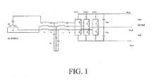
- FIG. 1 a schematic representation of a voltage source version of a Vienna-type active rectifier.
- a Vienna-type rectifier is a unidirectional three-phase three-switch three-level pulse-width modulation (PWM) rectifier.
- PWM pulse-width modulation
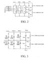
- a voltage source version of a Vienna-type active rectifier in series with an impedance can be interpreted as a current source, as illustrated in Fig. 2 .
- the current diagram of Fig. 2 can be further simplified to illustrate the current injection into the top-half and bottom-half of the DC bus. From this diagram, those skilled in the art will readily appreciate why the third order harmonic ripples appear on both halves of the DC bus and the two third harmonic voltage ripples are out-of-phase with each other.
- Fig. 4 illustrates the top and bottom halves of the DC bus voltage with third order harmonic ripples 180° out of phase from each other.
- the input frequency is 360 Hz
- C out is 200 ⁇ F
- the R out is 8.04.
- Fig. 5 shows the block diagram of a Vienna-type rectifier in which a controller and a PWM modulator are included.
- PWM pulse width modulator
- Fig. 6 there is illustrated the block diagram of a prior art PWM modulator for an active rectifier system as shown in Fig. 5 , with the two signals of "upper” and “lower” triangular waveforms shown in Fig. 6A . That is, prior to modification in accordance with the subject invention.
- the logic output for the comparator block is as follows:
- Fig. 7 illustrates a block diagram model of a PWM modulator that has been modified in accordance with the subject invention.
- the voltages of the top and bottom halves of the DC bus are sensed and then fed-forward into the pulse-width-modulation (PWM) modulator.
- PWM pulse-width-modulation
- the reference value for each phase from the controller is then rescaled using the two scale factors [Vdc_px] and [Vdc_nx]. This is done by multiplying the two scale factors [Vdc_px] and [Vdc_nx] by the reference value from the controller.
- the PWM command signal for each phase is scaled up (increased) when the corresponding half DC bus is decreased by the ripple and scaled down (decreased) when that DC half is increased by the ripple.
- the positive side of the PWM command corresponds to the top half of the DC bus and the negative side of that PWM command corresponds to the bottom half of the DC bus.
- Fig. 10 there is illustrated a single phase (Phase A) illustration of another well-known three-phase circuit topology of the Vienna-type rectifier in which the harmonic reduction method of the subject invention is also applied. More particularly, Fig. 10 illustrates a basic Y-clamped active rectifier that includes two clamped SiC Schottky diodes (D1 and D2) and a bidirectional switch containing two pairs of SiC Schottky diodes and SiC MOSFETs connected in parallel (S1 and S2).
Landscapes
- Engineering & Computer Science (AREA)
- Power Engineering (AREA)
- Rectifiers (AREA)
Applications Claiming Priority (1)
| Application Number | Priority Date | Filing Date | Title |
|---|---|---|---|
| US13/918,516 US9293985B2 (en) | 2013-06-14 | 2013-06-14 | Method of reducing input current distortion in a rectifier |
Publications (2)
| Publication Number | Publication Date |
|---|---|
| EP2814154A1 true EP2814154A1 (fr) | 2014-12-17 |
| EP2814154B1 EP2814154B1 (fr) | 2020-10-28 |
Family
ID=51022740
Family Applications (1)
| Application Number | Title | Priority Date | Filing Date |
|---|---|---|---|
| EP14172211.6A Active EP2814154B1 (fr) | 2013-06-14 | 2014-06-12 | Procédé de réduction de la distorsion de courant d'entrée dans un redresseur |
Country Status (2)
| Country | Link |
|---|---|
| US (1) | US9293985B2 (fr) |
| EP (1) | EP2814154B1 (fr) |
Families Citing this family (12)
| Publication number | Priority date | Publication date | Assignee | Title |
|---|---|---|---|---|
| US11043880B2 (en) | 2016-11-10 | 2021-06-22 | Hamilton Sunstrand Corporation | Electric power generating system with a synchronous generator |
| US10498274B2 (en) | 2016-11-10 | 2019-12-03 | Hamilton Sundstrand Corporation | High voltage direct current system for a vehicle |
| US20180191229A1 (en) * | 2017-01-03 | 2018-07-05 | Hamilton Sundstrand Corporation | Electric power generating system with a permanent magnet generator |
| CN112005482B (zh) * | 2018-04-27 | 2023-12-12 | 东芝三菱电机产业系统株式会社 | 三电平电力变换装置、三电平电力变换装置的控制方法及存储介质 |
| US10658919B1 (en) * | 2019-02-25 | 2020-05-19 | Hamilton Sundstrand Corporation | Harmonic regulator with loop delay compensation |
| CN111541382B (zh) * | 2020-04-30 | 2022-06-21 | 南京理工大学 | 一种针对大负载情况下Vienna整流器电流畸变的控制方法 |
| CN112600447B (zh) * | 2020-11-25 | 2023-02-28 | 深圳市科华恒盛科技有限公司 | 整流模组的应用方法 |
| CN112532025B (zh) * | 2020-12-03 | 2022-07-19 | 南京理工大学 | 一种用于在电网受干扰时优化Vienna整流器输入电流的方法 |
| CN112701939B (zh) * | 2020-12-07 | 2022-05-24 | 华南理工大学 | Vienna整流器电流预测控制方法 |
| CN112636614A (zh) * | 2020-12-16 | 2021-04-09 | 哈尔滨理工大学 | 一种新型三电平Delta型接法整流器 |
| CN112636618B (zh) * | 2020-12-23 | 2022-10-21 | 合肥工业大学 | 一种降低vienna整流器电流过零点畸变的调制方法 |
| EP4432532A1 (fr) | 2023-03-13 | 2024-09-18 | Goodrich Control Systems | Point de consigne pondere pour la stabilite active d'un redresseur |
Citations (3)
| Publication number | Priority date | Publication date | Assignee | Title |
|---|---|---|---|---|
| US5892674A (en) * | 1996-02-16 | 1999-04-06 | Hitachi, Ltd. | Method and apparatus for power converting AC into DC or DC into AC by converter having common phase connection |
| EP2509209A2 (fr) * | 2011-04-05 | 2012-10-10 | Hamilton Sundstrand Corporation | Redresseur actif avec un équilibrage de tension des condensateurs de sortie |
| EP2528221A2 (fr) * | 2011-05-26 | 2012-11-28 | Hamilton Sundstrand Corporation | Redresseur actif à phases multiples |
Family Cites Families (2)
| Publication number | Priority date | Publication date | Assignee | Title |
|---|---|---|---|---|
| BR9907351A (pt) * | 1999-12-22 | 2001-08-07 | Ericsson Telecomunicacoees S A | Método e circuito de controle para retificador do tipo elevador trifásico de três nìveis |
| US7196919B2 (en) * | 2005-03-25 | 2007-03-27 | Tyco Electronics Power Systems, Inc. | Neutral point controller, method of controlling and rectifier system employing the controller and the method |
-
2013
- 2013-06-14 US US13/918,516 patent/US9293985B2/en active Active
-
2014
- 2014-06-12 EP EP14172211.6A patent/EP2814154B1/fr active Active
Patent Citations (3)
| Publication number | Priority date | Publication date | Assignee | Title |
|---|---|---|---|---|
| US5892674A (en) * | 1996-02-16 | 1999-04-06 | Hitachi, Ltd. | Method and apparatus for power converting AC into DC or DC into AC by converter having common phase connection |
| EP2509209A2 (fr) * | 2011-04-05 | 2012-10-10 | Hamilton Sundstrand Corporation | Redresseur actif avec un équilibrage de tension des condensateurs de sortie |
| EP2528221A2 (fr) * | 2011-05-26 | 2012-11-28 | Hamilton Sundstrand Corporation | Redresseur actif à phases multiples |
Non-Patent Citations (1)
| Title |
|---|
| ANONYMOUS: "A number from a set divided by the average of the set?", 31 January 2007 (2007-01-31), XP002731513, Retrieved from the Internet <URL:http://askville.amazon.com/number-set-divided-average/AnswerViewer.do?requestId=1036602> [retrieved on 20141023] * |
Also Published As
| Publication number | Publication date |
|---|---|
| US9293985B2 (en) | 2016-03-22 |
| EP2814154B1 (fr) | 2020-10-28 |
| US20140369092A1 (en) | 2014-12-18 |
Similar Documents
| Publication | Publication Date | Title |
|---|---|---|
| US9293985B2 (en) | Method of reducing input current distortion in a rectifier | |
| US9948200B2 (en) | Charge and discharge circuit, control method for charge and discharge circuit, control device for charge and discharge circuit, and direct power converter | |
| CN105900326B (zh) | 转换装置 | |
| CN104704733B (zh) | 直接型电力转换装置以及直接型电力转换装置的控制方法 | |
| US10804811B2 (en) | Control device for direct power converter for reduction of harmonic distortion | |
| US11177741B2 (en) | AC-AC converter circuit | |
| US11437921B2 (en) | Direct power converter and control device to improve an input power factor | |
| Le et al. | Inductance-independent nonlinearity compensation for single-phase grid-tied inverter operating in both continuous and discontinuous current mode | |
| Ji et al. | Dual-loop control for three-phase Vienna rectifier with duty-ratio feedforward | |
| Adamowicz et al. | Advances in CSI-fed induction motor drives | |
| Suhara et al. | Novel adaptive hysteresis current control of bidirectional three phase PWM converter under reduced switching scheme | |
| Maswood et al. | Analysis of a PWM Voltage Source Inverter with PI Controller under Non-ideal conditions | |
| JP4839729B2 (ja) | Ac−dc変換装置 | |
| Sabrié et al. | Investigation of the modulation index tuning advantages for voltage source inverters with adjustable DC-bus voltage | |
| Lee et al. | DC link voltage controller for three phase vienna rectifier with compensated load current and duty | |
| Sajeesh et al. | Power factor improvement in rectifier circuit—A simulation study | |
| CN112564520A (zh) | 一种pwm信号的调制方法和系统 | |
| Yoneda et al. | Switching loss reduction of AC-AC converter using three-level rectifier and inverter for UPS | |
| Ahmad et al. | Modified modulation signals for GaN-E-HEMTs based HERIC inverter to improve reverse conduction performance | |
| Bakar et al. | Analysis of various PWM controls on single-phase Z-source inverter | |
| Fathipour et al. | A Single-Phase Boost AC-AC Converter with Inherent Commutation and Step-Changed Frequency Operation | |
| Leontaris et al. | Three-Leg Operation of Back-to-Back Converters | |
| Ursaru et al. | Multilevel Inverters with Imbricated Switching Cells, PWM and DPWM-Controlled | |
| Wang et al. | Dc-bus voltage control of three-phase ac/dc converter using load predictive method | |
| Akila et al. | Analysis of closed loop single phase z-source buck and boost matrix converter with reduced number of switches Using PI Controller |
Legal Events
| Date | Code | Title | Description |
|---|---|---|---|
| 17P | Request for examination filed |
Effective date: 20140612 |
|
| AK | Designated contracting states |
Kind code of ref document: A1 Designated state(s): AL AT BE BG CH CY CZ DE DK EE ES FI FR GB GR HR HU IE IS IT LI LT LU LV MC MK MT NL NO PL PT RO RS SE SI SK SM TR |
|
| AX | Request for extension of the european patent |
Extension state: BA ME |
|
| PUAI | Public reference made under article 153(3) epc to a published international application that has entered the european phase |
Free format text: ORIGINAL CODE: 0009012 |
|
| R17P | Request for examination filed (corrected) |
Effective date: 20150617 |
|
| RBV | Designated contracting states (corrected) |
Designated state(s): AL AT BE BG CH CY CZ DE DK EE ES FI FR GB GR HR HU IE IS IT LI LT LU LV MC MK MT NL NO PL PT RO RS SE SI SK SM TR |
|
| STAA | Information on the status of an ep patent application or granted ep patent |
Free format text: STATUS: EXAMINATION IS IN PROGRESS |
|
| 17Q | First examination report despatched |
Effective date: 20180829 |
|
| GRAP | Despatch of communication of intention to grant a patent |
Free format text: ORIGINAL CODE: EPIDOSNIGR1 |
|
| STAA | Information on the status of an ep patent application or granted ep patent |
Free format text: STATUS: GRANT OF PATENT IS INTENDED |
|
| INTG | Intention to grant announced |
Effective date: 20200520 |
|
| GRAS | Grant fee paid |
Free format text: ORIGINAL CODE: EPIDOSNIGR3 |
|
| GRAA | (expected) grant |
Free format text: ORIGINAL CODE: 0009210 |
|
| STAA | Information on the status of an ep patent application or granted ep patent |
Free format text: STATUS: THE PATENT HAS BEEN GRANTED |
|
| AK | Designated contracting states |
Kind code of ref document: B1 Designated state(s): AL AT BE BG CH CY CZ DE DK EE ES FI FR GB GR HR HU IE IS IT LI LT LU LV MC MK MT NL NO PL PT RO RS SE SI SK SM TR |
|
| REG | Reference to a national code |
Ref country code: GB Ref legal event code: FG4D |
|
| REG | Reference to a national code |
Ref country code: CH Ref legal event code: EP |
|
| REG | Reference to a national code |
Ref country code: DE Ref legal event code: R096 Ref document number: 602014071634 Country of ref document: DE |
|
| REG | Reference to a national code |
Ref country code: AT Ref legal event code: REF Ref document number: 1329232 Country of ref document: AT Kind code of ref document: T Effective date: 20201115 |
|
| REG | Reference to a national code |
Ref country code: IE Ref legal event code: FG4D |
|
| REG | Reference to a national code |
Ref country code: AT Ref legal event code: MK05 Ref document number: 1329232 Country of ref document: AT Kind code of ref document: T Effective date: 20201028 |
|
| REG | Reference to a national code |
Ref country code: NL Ref legal event code: MP Effective date: 20201028 |
|
| PG25 | Lapsed in a contracting state [announced via postgrant information from national office to epo] |
Ref country code: GR Free format text: LAPSE BECAUSE OF FAILURE TO SUBMIT A TRANSLATION OF THE DESCRIPTION OR TO PAY THE FEE WITHIN THE PRESCRIBED TIME-LIMIT Effective date: 20210129 Ref country code: FI Free format text: LAPSE BECAUSE OF FAILURE TO SUBMIT A TRANSLATION OF THE DESCRIPTION OR TO PAY THE FEE WITHIN THE PRESCRIBED TIME-LIMIT Effective date: 20201028 Ref country code: RS Free format text: LAPSE BECAUSE OF FAILURE TO SUBMIT A TRANSLATION OF THE DESCRIPTION OR TO PAY THE FEE WITHIN THE PRESCRIBED TIME-LIMIT Effective date: 20201028 Ref country code: NO Free format text: LAPSE BECAUSE OF FAILURE TO SUBMIT A TRANSLATION OF THE DESCRIPTION OR TO PAY THE FEE WITHIN THE PRESCRIBED TIME-LIMIT Effective date: 20210128 Ref country code: PT Free format text: LAPSE BECAUSE OF FAILURE TO SUBMIT A TRANSLATION OF THE DESCRIPTION OR TO PAY THE FEE WITHIN THE PRESCRIBED TIME-LIMIT Effective date: 20210301 Ref country code: NL Free format text: LAPSE BECAUSE OF FAILURE TO SUBMIT A TRANSLATION OF THE DESCRIPTION OR TO PAY THE FEE WITHIN THE PRESCRIBED TIME-LIMIT Effective date: 20201028 |
|
| REG | Reference to a national code |
Ref country code: LT Ref legal event code: MG4D |
|
| PG25 | Lapsed in a contracting state [announced via postgrant information from national office to epo] |
Ref country code: ES Free format text: LAPSE BECAUSE OF FAILURE TO SUBMIT A TRANSLATION OF THE DESCRIPTION OR TO PAY THE FEE WITHIN THE PRESCRIBED TIME-LIMIT Effective date: 20201028 Ref country code: AT Free format text: LAPSE BECAUSE OF FAILURE TO SUBMIT A TRANSLATION OF THE DESCRIPTION OR TO PAY THE FEE WITHIN THE PRESCRIBED TIME-LIMIT Effective date: 20201028 Ref country code: BG Free format text: LAPSE BECAUSE OF FAILURE TO SUBMIT A TRANSLATION OF THE DESCRIPTION OR TO PAY THE FEE WITHIN THE PRESCRIBED TIME-LIMIT Effective date: 20210128 Ref country code: LV Free format text: LAPSE BECAUSE OF FAILURE TO SUBMIT A TRANSLATION OF THE DESCRIPTION OR TO PAY THE FEE WITHIN THE PRESCRIBED TIME-LIMIT Effective date: 20201028 Ref country code: PL Free format text: LAPSE BECAUSE OF FAILURE TO SUBMIT A TRANSLATION OF THE DESCRIPTION OR TO PAY THE FEE WITHIN THE PRESCRIBED TIME-LIMIT Effective date: 20201028 Ref country code: SE Free format text: LAPSE BECAUSE OF FAILURE TO SUBMIT A TRANSLATION OF THE DESCRIPTION OR TO PAY THE FEE WITHIN THE PRESCRIBED TIME-LIMIT Effective date: 20201028 Ref country code: IS Free format text: LAPSE BECAUSE OF FAILURE TO SUBMIT A TRANSLATION OF THE DESCRIPTION OR TO PAY THE FEE WITHIN THE PRESCRIBED TIME-LIMIT Effective date: 20210228 |
|
| PG25 | Lapsed in a contracting state [announced via postgrant information from national office to epo] |
Ref country code: HR Free format text: LAPSE BECAUSE OF FAILURE TO SUBMIT A TRANSLATION OF THE DESCRIPTION OR TO PAY THE FEE WITHIN THE PRESCRIBED TIME-LIMIT Effective date: 20201028 |
|
| REG | Reference to a national code |
Ref country code: DE Ref legal event code: R097 Ref document number: 602014071634 Country of ref document: DE |
|
| PG25 | Lapsed in a contracting state [announced via postgrant information from national office to epo] |
Ref country code: SM Free format text: LAPSE BECAUSE OF FAILURE TO SUBMIT A TRANSLATION OF THE DESCRIPTION OR TO PAY THE FEE WITHIN THE PRESCRIBED TIME-LIMIT Effective date: 20201028 Ref country code: EE Free format text: LAPSE BECAUSE OF FAILURE TO SUBMIT A TRANSLATION OF THE DESCRIPTION OR TO PAY THE FEE WITHIN THE PRESCRIBED TIME-LIMIT Effective date: 20201028 Ref country code: CZ Free format text: LAPSE BECAUSE OF FAILURE TO SUBMIT A TRANSLATION OF THE DESCRIPTION OR TO PAY THE FEE WITHIN THE PRESCRIBED TIME-LIMIT Effective date: 20201028 Ref country code: LT Free format text: LAPSE BECAUSE OF FAILURE TO SUBMIT A TRANSLATION OF THE DESCRIPTION OR TO PAY THE FEE WITHIN THE PRESCRIBED TIME-LIMIT Effective date: 20201028 Ref country code: RO Free format text: LAPSE BECAUSE OF FAILURE TO SUBMIT A TRANSLATION OF THE DESCRIPTION OR TO PAY THE FEE WITHIN THE PRESCRIBED TIME-LIMIT Effective date: 20201028 Ref country code: SK Free format text: LAPSE BECAUSE OF FAILURE TO SUBMIT A TRANSLATION OF THE DESCRIPTION OR TO PAY THE FEE WITHIN THE PRESCRIBED TIME-LIMIT Effective date: 20201028 |
|
| PG25 | Lapsed in a contracting state [announced via postgrant information from national office to epo] |
Ref country code: DK Free format text: LAPSE BECAUSE OF FAILURE TO SUBMIT A TRANSLATION OF THE DESCRIPTION OR TO PAY THE FEE WITHIN THE PRESCRIBED TIME-LIMIT Effective date: 20201028 |
|
| PLBE | No opposition filed within time limit |
Free format text: ORIGINAL CODE: 0009261 |
|
| STAA | Information on the status of an ep patent application or granted ep patent |
Free format text: STATUS: NO OPPOSITION FILED WITHIN TIME LIMIT |
|
| 26N | No opposition filed |
Effective date: 20210729 |
|
| PG25 | Lapsed in a contracting state [announced via postgrant information from national office to epo] |
Ref country code: AL Free format text: LAPSE BECAUSE OF FAILURE TO SUBMIT A TRANSLATION OF THE DESCRIPTION OR TO PAY THE FEE WITHIN THE PRESCRIBED TIME-LIMIT Effective date: 20201028 Ref country code: IT Free format text: LAPSE BECAUSE OF FAILURE TO SUBMIT A TRANSLATION OF THE DESCRIPTION OR TO PAY THE FEE WITHIN THE PRESCRIBED TIME-LIMIT Effective date: 20201028 |
|
| PG25 | Lapsed in a contracting state [announced via postgrant information from national office to epo] |
Ref country code: SI Free format text: LAPSE BECAUSE OF FAILURE TO SUBMIT A TRANSLATION OF THE DESCRIPTION OR TO PAY THE FEE WITHIN THE PRESCRIBED TIME-LIMIT Effective date: 20201028 |
|
| PG25 | Lapsed in a contracting state [announced via postgrant information from national office to epo] |
Ref country code: MC Free format text: LAPSE BECAUSE OF FAILURE TO SUBMIT A TRANSLATION OF THE DESCRIPTION OR TO PAY THE FEE WITHIN THE PRESCRIBED TIME-LIMIT Effective date: 20201028 |
|
| REG | Reference to a national code |
Ref country code: CH Ref legal event code: PL |
|
| REG | Reference to a national code |
Ref country code: BE Ref legal event code: MM Effective date: 20210630 |
|
| PG25 | Lapsed in a contracting state [announced via postgrant information from national office to epo] |
Ref country code: LU Free format text: LAPSE BECAUSE OF NON-PAYMENT OF DUE FEES Effective date: 20210612 |
|
| PG25 | Lapsed in a contracting state [announced via postgrant information from national office to epo] |
Ref country code: LI Free format text: LAPSE BECAUSE OF NON-PAYMENT OF DUE FEES Effective date: 20210630 Ref country code: IE Free format text: LAPSE BECAUSE OF NON-PAYMENT OF DUE FEES Effective date: 20210612 Ref country code: CH Free format text: LAPSE BECAUSE OF NON-PAYMENT OF DUE FEES Effective date: 20210630 |
|
| PG25 | Lapsed in a contracting state [announced via postgrant information from national office to epo] |
Ref country code: IS Free format text: LAPSE BECAUSE OF FAILURE TO SUBMIT A TRANSLATION OF THE DESCRIPTION OR TO PAY THE FEE WITHIN THE PRESCRIBED TIME-LIMIT Effective date: 20210228 |
|
| PG25 | Lapsed in a contracting state [announced via postgrant information from national office to epo] |
Ref country code: BE Free format text: LAPSE BECAUSE OF NON-PAYMENT OF DUE FEES Effective date: 20210630 |
|
| PG25 | Lapsed in a contracting state [announced via postgrant information from national office to epo] |
Ref country code: HU Free format text: LAPSE BECAUSE OF FAILURE TO SUBMIT A TRANSLATION OF THE DESCRIPTION OR TO PAY THE FEE WITHIN THE PRESCRIBED TIME-LIMIT; INVALID AB INITIO Effective date: 20140612 |
|
| P01 | Opt-out of the competence of the unified patent court (upc) registered |
Effective date: 20230522 |
|
| PG25 | Lapsed in a contracting state [announced via postgrant information from national office to epo] |
Ref country code: CY Free format text: LAPSE BECAUSE OF FAILURE TO SUBMIT A TRANSLATION OF THE DESCRIPTION OR TO PAY THE FEE WITHIN THE PRESCRIBED TIME-LIMIT Effective date: 20201028 |
|
| PG25 | Lapsed in a contracting state [announced via postgrant information from national office to epo] |
Ref country code: MK Free format text: LAPSE BECAUSE OF FAILURE TO SUBMIT A TRANSLATION OF THE DESCRIPTION OR TO PAY THE FEE WITHIN THE PRESCRIBED TIME-LIMIT Effective date: 20201028 |
|
| PG25 | Lapsed in a contracting state [announced via postgrant information from national office to epo] |
Ref country code: MT Free format text: LAPSE BECAUSE OF FAILURE TO SUBMIT A TRANSLATION OF THE DESCRIPTION OR TO PAY THE FEE WITHIN THE PRESCRIBED TIME-LIMIT Effective date: 20201028 |
|
| PGFP | Annual fee paid to national office [announced via postgrant information from national office to epo] |
Ref country code: DE Payment date: 20250520 Year of fee payment: 12 |
|
| PGFP | Annual fee paid to national office [announced via postgrant information from national office to epo] |
Ref country code: GB Payment date: 20250520 Year of fee payment: 12 |
|
| PGFP | Annual fee paid to national office [announced via postgrant information from national office to epo] |
Ref country code: FR Payment date: 20250520 Year of fee payment: 12 |
|
| PG25 | Lapsed in a contracting state [announced via postgrant information from national office to epo] |
Ref country code: TR Free format text: LAPSE BECAUSE OF FAILURE TO SUBMIT A TRANSLATION OF THE DESCRIPTION OR TO PAY THE FEE WITHIN THE PRESCRIBED TIME-LIMIT Effective date: 20201028 |