EP2525399A1 - Kristallvorrichtung ohne kapselung und herstellungsverfahren dafür - Google Patents
Kristallvorrichtung ohne kapselung und herstellungsverfahren dafür Download PDFInfo
- Publication number
- EP2525399A1 EP2525399A1 EP10856616A EP10856616A EP2525399A1 EP 2525399 A1 EP2525399 A1 EP 2525399A1 EP 10856616 A EP10856616 A EP 10856616A EP 10856616 A EP10856616 A EP 10856616A EP 2525399 A1 EP2525399 A1 EP 2525399A1
- Authority
- EP
- European Patent Office
- Prior art keywords
- pins
- crystal
- pcb
- welding
- package
- Prior art date
- Legal status (The legal status is an assumption and is not a legal conclusion. Google has not performed a legal analysis and makes no representation as to the accuracy of the status listed.)
- Withdrawn
Links
Images


Classifications
-
- H—ELECTRICITY
- H05—ELECTRIC TECHNIQUES NOT OTHERWISE PROVIDED FOR
- H05K—PRINTED CIRCUITS; CASINGS OR CONSTRUCTIONAL DETAILS OF ELECTRIC APPARATUS; MANUFACTURE OF ASSEMBLAGES OF ELECTRICAL COMPONENTS
- H05K3/00—Apparatus or processes for manufacturing printed circuits
- H05K3/30—Assembling printed circuits with electric components, e.g. with resistors
- H05K3/32—Assembling printed circuits with electric components, e.g. with resistors electrically connecting electric components or wires to printed circuits
- H05K3/34—Assembling printed circuits with electric components, e.g. with resistors electrically connecting electric components or wires to printed circuits by soldering
- H05K3/341—Surface mounted components
- H05K3/3421—Leaded components
- H05K3/3426—Leaded components characterised by the leads
-
- H—ELECTRICITY
- H03—ELECTRONIC CIRCUITRY
- H03H—IMPEDANCE NETWORKS, e.g. RESONANT CIRCUITS; RESONATORS
- H03H9/00—Networks comprising electromechanical or electro-acoustic elements; Electromechanical resonators
- H03H9/02—Details
- H03H9/05—Holders or supports
- H03H9/10—Mounting in enclosures
- H03H9/1007—Mounting in enclosures for bulk acoustic wave [BAW] devices
-
- H—ELECTRICITY
- H05—ELECTRIC TECHNIQUES NOT OTHERWISE PROVIDED FOR
- H05K—PRINTED CIRCUITS; CASINGS OR CONSTRUCTIONAL DETAILS OF ELECTRIC APPARATUS; MANUFACTURE OF ASSEMBLAGES OF ELECTRICAL COMPONENTS
- H05K2201/00—Indexing scheme relating to printed circuits covered by H05K1/00
- H05K2201/10—Details of components or other objects attached to or integrated in a printed circuit board
- H05K2201/10007—Types of components
- H05K2201/10068—Non-printed resonator
-
- H—ELECTRICITY
- H05—ELECTRIC TECHNIQUES NOT OTHERWISE PROVIDED FOR
- H05K—PRINTED CIRCUITS; CASINGS OR CONSTRUCTIONAL DETAILS OF ELECTRIC APPARATUS; MANUFACTURE OF ASSEMBLAGES OF ELECTRICAL COMPONENTS
- H05K2201/00—Indexing scheme relating to printed circuits covered by H05K1/00
- H05K2201/10—Details of components or other objects attached to or integrated in a printed circuit board
- H05K2201/10007—Types of components
- H05K2201/10075—Non-printed oscillator
-
- H—ELECTRICITY
- H05—ELECTRIC TECHNIQUES NOT OTHERWISE PROVIDED FOR
- H05K—PRINTED CIRCUITS; CASINGS OR CONSTRUCTIONAL DETAILS OF ELECTRIC APPARATUS; MANUFACTURE OF ASSEMBLAGES OF ELECTRICAL COMPONENTS
- H05K2201/00—Indexing scheme relating to printed circuits covered by H05K1/00
- H05K2201/10—Details of components or other objects attached to or integrated in a printed circuit board
- H05K2201/10431—Details of mounted components
- H05K2201/10439—Position of a single component
- H05K2201/10462—Flat component oriented parallel to the PCB surface
-
- H—ELECTRICITY
- H05—ELECTRIC TECHNIQUES NOT OTHERWISE PROVIDED FOR
- H05K—PRINTED CIRCUITS; CASINGS OR CONSTRUCTIONAL DETAILS OF ELECTRIC APPARATUS; MANUFACTURE OF ASSEMBLAGES OF ELECTRICAL COMPONENTS
- H05K3/00—Apparatus or processes for manufacturing printed circuits
- H05K3/30—Assembling printed circuits with electric components, e.g. with resistors
- H05K3/32—Assembling printed circuits with electric components, e.g. with resistors electrically connecting electric components or wires to printed circuits
- H05K3/34—Assembling printed circuits with electric components, e.g. with resistors electrically connecting electric components or wires to printed circuits by soldering
- H05K3/3494—Heating processes for reflow soldering
-
- Y—GENERAL TAGGING OF NEW TECHNOLOGICAL DEVELOPMENTS; GENERAL TAGGING OF CROSS-SECTIONAL TECHNOLOGIES SPANNING OVER SEVERAL SECTIONS OF THE IPC; TECHNICAL SUBJECTS COVERED BY FORMER USPC CROSS-REFERENCE ART COLLECTIONS [XRACs] AND DIGESTS
- Y02—TECHNOLOGIES OR APPLICATIONS FOR MITIGATION OR ADAPTATION AGAINST CLIMATE CHANGE
- Y02P—CLIMATE CHANGE MITIGATION TECHNOLOGIES IN THE PRODUCTION OR PROCESSING OF GOODS
- Y02P70/00—Climate change mitigation technologies in the production process for final industrial or consumer products
- Y02P70/50—Manufacturing or production processes characterised by the final manufactured product
-
- Y—GENERAL TAGGING OF NEW TECHNOLOGICAL DEVELOPMENTS; GENERAL TAGGING OF CROSS-SECTIONAL TECHNOLOGIES SPANNING OVER SEVERAL SECTIONS OF THE IPC; TECHNICAL SUBJECTS COVERED BY FORMER USPC CROSS-REFERENCE ART COLLECTIONS [XRACs] AND DIGESTS
- Y10—TECHNICAL SUBJECTS COVERED BY FORMER USPC
- Y10T—TECHNICAL SUBJECTS COVERED BY FORMER US CLASSIFICATION
- Y10T29/00—Metal working
- Y10T29/49—Method of mechanical manufacture
- Y10T29/49002—Electrical device making
- Y10T29/49117—Conductor or circuit manufacturing
- Y10T29/49124—On flat or curved insulated base, e.g., printed circuit, etc.
Definitions
- the disclosure relates to the field of crystal manufacturing and assembly, particularly to a crystal device without an external package and a manufacturing method thereof.
- the technical innovation of product and the characteristic of craft are the key for the success of competition.
- the main object of the technical innovation is to improve performance of the product
- the characteristic improvement of the craft is to reduce the cost of the product; only when the cost is reduced can the sale price be reduced and the product be more competitive.
- the manufacturer must take into account the performance and quality of the product so as to try to meet the experience of the user.
- 32K crystal is a common electronic device.
- the parameter of the 32K crystal is as follows: frequency: 32.768KHz, load capacitance: 12.5pF, level of drive: 1.0 ⁇ W Max, frequency tolerance: ⁇ 20ppm.
- the 32K crystal uses a plastic package as an external package and has smaller pins; in addition, the crystal shell inside the resin package shell probably partially exposes out, which cannot get an effect of 100% perfect package. In order to paste more conveniently when the package, two pins are needed to be added for balance the crystals; in this way, the complexity of pins and package would be increased, thus the manufacturing cost of the product is increased.
- the main object of the disclosure is to provide a crystal device without an external package and a manufacturing method thereof, with a capability of reducing the manufacturing cost of the 32K crystal and making welding more convenient.
- the disclosure provides a crystal device without an external package, which comprises: a crystal body and two pins, in which, the crystal body is a cylindrical body port of a crystal with the external package and redundant pins being removed, and is arranged on a Printed Circuit Board (PCB) horizontally; and the two pins are connected to a bottom end of the crystal body; extension parts of the two pins are inclined towards the PCB, and become horizontal when they reach the PCB and are welded to the PCB; and a spacing between the two pins increases gradually.
- PCB Printed Circuit Board
- the welding may be performed by using a reflow soldering oven.
- the extension parts of the two pins may be inclined towards the PCB with an angle of 90 degrees to 100 degrees for each pin.
- the redundant pins may be pins added into the original external package for balance.
- the disclosure further provides a method for manufacturing a crystal device without a package, which comprises:
- the welding may be performed by using a reflow soldering oven, the welding process may comprise: during the welding by using the reflow soldering oven, an initial temperature of the PCB is 50 ⁇ , the temperature of the reflow soldering oven rises straightly to 170 ⁇ 10 ⁇ within 50 seconds at a slope of 2.2 to 2.6, then maintains for 120 ⁇ 20 seconds, then rises straightly again to 250 ⁇ within 50 seconds at a slope of 1.3 to 2, then rises from 250 ⁇ to a highest temperature 260 ⁇ within 5 seconds, then begins to decrease from the highest temperature 260 ⁇ to 220 ⁇ at a slope of -2 to -1.3, and then the patch welding of the crystal is completed.
- the extension parts of the two pins may be inclined towards the PCB with an angle of 90 degrees to 100 degrees for each pin.
- the crystal device without an external package and the manufacturing method thereof provided by the disclosure remove the external package and redundant pins of the 32K crystal with a plastic package to expose a cylindrical crystal body and place it on a PCB horizontally, wherein two pins are extended from a bottom end of the crystal body horizontally and are inclined towards the PCB, and then become horizontal when they reach the PCB and are welded to the PCB, wherein the spacing between the two pins increases gradually when inclining.
- the manufacturing cost is reduced; in addition, while the two pins are inclined towards the PCB, the distance there-between increases gradually, thus welding is more convenient.
- Fig. 1 is a structure diagram of a 32K crystal with a plastic package; as shown in Fig. 1 , the above one is a side view of a 32K crystal; the lower one is a bottom view of the 32K crystal; the 32K crystal comprises: a pin 11, a pin 12, a pin 13, a pin 14 and a plastic package 15, wherein the pin 12 and the pin 13 are added for balance; the pin 11 and the pin 14 are the useful pins to which the 32K crystal are actually connected; a shell of the crystal is encapsulated with the plastic package 15.
- the basic idea of the disclosure is: removing the external package and redundant pins of a 32K crystal with a plastic package to expose a crystal body and placing it on a PCB horizontally; extending two pins from a bottom end of the crystal body horizontally, wherein the extension parts of the two pins are inclined towards the PCB, and then become horizontal when they reach the PCB and are welded to the PCB, and a spacing between the two pins increases gradually when inclining.
- Fig. 2 is a structure diagram of a crystal device without an external package according to the disclosure; as shown in Fig. 2 , the crystal without the external package mainly refers to a 32K crystal, wherein the crystal comprises: a crystal body 21 and two pins 22, in which,
- the crystal body 21 is a cylindrical body port of a crystal with the external package and redundant pins being removed, and is arranged on a PCB horizontally;
- the redundant pins specifically refer to the pins added into the original external package for balance; for example, the pin 12 and the pin 13 in Fig. 1 .
- the shell material of the crystal body is the material commonly adopted by a Surface Mounted Technology (SMT), for example: ceramic, resin, etc.
- SMT Surface Mounted Technology
- the two pins 22 are connected to a bottom end of the crystal body 21, extension parts of the two pins are inclined towards the PCB, and become horizontal when they reach the PCB and are welded to the PCB; and a spacing between the two pins 22 increases gradually when inclining.
- the two pins both are of metal material. Since the crystal body 21 is cylindrical, the two pins 22 connected to the bottom end of the cylinder cannot be welded to the PCB directly; therefore, the pins need to incline towards the PCB, wherein the inclining angle of the pin preferably is between 90 degrees and 100 degrees; while the two pins 22 are inclining, the spacing between the two pins increases gradually, so as to increase the spacing between the pins during welding, thus the welding or demounting is more convenient and the bad welding, caused when the pins are too near, can be avoided.
- Fig. 3 is a preferred temperature control curve for a reflow soldering oven according to the disclosure; as shown in Fig.
- the initial temperature of the PCB is about 50 ⁇ ; the temperature of the reflow soldering oven rises straightly to 170 ⁇ 10 ⁇ within about 50 seconds at a slope of 2.2 to 2.6, then maintains for 120 ⁇ 20 seconds; at this moment, the total time consumed is about 150 to 190 seconds, then the temperature rises straightly again to 250 ⁇ within about 50 seconds at a slope of 1.3 to 2; then rises from 250 ⁇ to a highest temperature 260°C within about 5 seconds; after reaching the highest temperature 260°C, the temperature begins to decrease, wherein the process of rising from 250°C to 260°C and decreasing from 260°C to 250°C last 10 ⁇ 1 seconds; then the temperature begins to decrease straightly from 250°C to 220°C at a slope of -2 to -1.3; then the patch welding of the crystal is completed.
- Fig. 4 is top views of two specifications of 32K crystals according to the disclosure; as shown in Fig. 4 , the above one is a top view of the 32K crystal with smaller specification, the length L1 of the cylindrical crystal body 21 is 4.7 mm, the diameter D1 of the bottom circular surface of the crystal body is 1.2 mm, the distance W1 from the ends of the two pins 22 to the bottom end of the crystal body 21 from which the pins are extended is 1.8 ⁇ 0.2 mm, the spacing Z1 between the ends of the two pins 22 is 1.3 ⁇ 0.2 mm, the tangent planes of the two pins 22 are circular, with diameter d1 of 0.22 ⁇ 0.05 mm.
- the lower one is a top view of the 32K crystal with bigger specification
- the length L2 of the cylindrical crystal body 21 is 6.0 ⁇ 0.2 mm
- the diameter D2 of the bottom circular surface is 2.0 ⁇ 0.1 mm
- the distance W2 from the ends of the two pins 22 to the bottom end of the crystal body 21 from which the pins are extended is 2.7 ⁇ 0.3 mm
- the spacing Z2 between the ends of the two pins 22 is 2.54 ⁇ 0.3 mm.
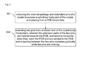
- Fig. 5 is a flowchart of a method for manufacturing a crystal device without a package according to the disclosure. As shown in Fig. 5 , the method for manufacturing the crystal device without the package comprises the following steps.
- Step 501 removing the external package and redundant pins of a crystal to expose a cylindrical body part of the crystal, and placing it on a PCB horizontally.
- the redundant pins specifically refer to pins added into the original external package for balance; for example, the pin 12 and the pin 13 in Fig. 1 .
- the shell material of the crystal body is the material commonly adopted by the SMT, for example: ceramic, resin, etc.
- Step 502 extending two pins from a bottom end of the crystal body horizontally, wherein the extension parts of the two pins are inclined towards the PCB, and become horizontal when they reach the PCB and are welded to the PCB, and a spacing between the two pins increases gradually while the pins are inclining.
- the two pins both are of metal material. Since the crystal body is cylindrical, the two pins extended horizontally from the bottom end of the cylinder cannot be welded to the PCB directly; therefore, the pins need to incline towards the PCB, wherein the inclining angle of the pin preferably is between 90 degrees and 100 degrees; while the two pins are inclining, the spacing between the two pins increases gradually, so as to increase the spacing between the pins during welding, thus the welding or demounting is more convenient and the bad welding, caused when the pins are too near, can be avoided.
- the welding preferably can be performed by using a reflow soldering oven, wherein the welding process needs to operate according to a preset temperature control curve to achieve the best effect.
- the welding process specifically comprises: first, the initial temperature of the PCB is 50°C; the temperature of the reflow soldering oven rises straightly to 170 ⁇ 10°C within 50 seconds at a slope of 2.2 to 2.6, then maintains for 120 ⁇ 20 seconds, then rises straightly again to 250°C within 50 seconds at a slope of 1.3 to 2; after rising to 250°C, the temperate rises to a highest temperature 260°C within 5 seconds; after reaching the highest temperature 260°C, the temperature begins to decrease straightly to 220°C at a slope of -2 to -1.3; then the patch welding of the crystal is completed.
Landscapes
- Engineering & Computer Science (AREA)
- Physics & Mathematics (AREA)
- Acoustics & Sound (AREA)
- Manufacturing & Machinery (AREA)
- Microelectronics & Electronic Packaging (AREA)
- Piezo-Electric Or Mechanical Vibrators, Or Delay Or Filter Circuits (AREA)
- Lead Frames For Integrated Circuits (AREA)
Applications Claiming Priority (2)
| Application Number | Priority Date | Filing Date | Title |
|---|---|---|---|
| CN2010102754946A CN101976659B (zh) | 2010-09-03 | 2010-09-03 | 一种无外封装晶体装置及其制造方法 |
| PCT/CN2010/078788 WO2012027929A1 (zh) | 2010-09-03 | 2010-11-16 | 一种无外封装晶体装置及其制造方法 |
Publications (2)
| Publication Number | Publication Date |
|---|---|
| EP2525399A1 true EP2525399A1 (de) | 2012-11-21 |
| EP2525399A4 EP2525399A4 (de) | 2016-11-23 |
Family
ID=43576529
Family Applications (1)
| Application Number | Title | Priority Date | Filing Date |
|---|---|---|---|
| EP10856616.7A Withdrawn EP2525399A4 (de) | 2010-09-03 | 2010-11-16 | Kristallvorrichtung ohne kapselung und herstellungsverfahren dafür |
Country Status (4)
| Country | Link |
|---|---|
| US (1) | US20120300424A1 (de) |
| EP (1) | EP2525399A4 (de) |
| CN (1) | CN101976659B (de) |
| WO (1) | WO2012027929A1 (de) |
Families Citing this family (4)
| Publication number | Priority date | Publication date | Assignee | Title |
|---|---|---|---|---|
| CN103028802A (zh) * | 2012-12-31 | 2013-04-10 | 北京中科同志科技有限公司 | 一种回流焊机温度控制方法 |
| US9420178B2 (en) * | 2013-12-20 | 2016-08-16 | Qualcomm Incorporated | Thermal and power management |
| CN104302102A (zh) * | 2014-09-26 | 2015-01-21 | 中国科学院长春光学精密机械与物理研究所 | 一种红外焦平面传感器无封装应用方法 |
| CN107195753A (zh) * | 2017-05-25 | 2017-09-22 | 宁波升谱光电股份有限公司 | 一种led及其制备方法 |
Family Cites Families (13)
| Publication number | Priority date | Publication date | Assignee | Title |
|---|---|---|---|---|
| US4116519A (en) * | 1977-08-02 | 1978-09-26 | Amp Incorporated | Electrical connections for chip carriers |
| JP2773087B2 (ja) * | 1991-03-26 | 1998-07-09 | アイワ株式会社 | 電子部品の実装方法 |
| JPH06151646A (ja) * | 1992-11-12 | 1994-05-31 | Canon Inc | Icパッケージ及び回路基板 |
| US5912592A (en) * | 1994-07-04 | 1999-06-15 | Seiko Epson Corporation | Piezoelectric oscillator |
| DE19649650B4 (de) * | 1996-11-29 | 2005-02-24 | Siemens Ag | Oberflächenmontierbares strahlungsemittierendes Halbleiterbauelement |
| JPH10276056A (ja) * | 1997-03-28 | 1998-10-13 | Seiko Instr Inc | 表面実装水晶振動子およびその製造方法 |
| JP2002217671A (ja) * | 2001-01-17 | 2002-08-02 | Miyota Kk | 振動子の接続部品、振動子ユニット及びその実装構造 |
| JP2002290188A (ja) * | 2001-03-28 | 2002-10-04 | Miyota Kk | 表面実装型水晶振動子 |
| JP3770210B2 (ja) * | 2002-06-20 | 2006-04-26 | 株式会社村田製作所 | 圧電部品の製造方法 |
| US6991110B2 (en) * | 2003-07-02 | 2006-01-31 | Inficon, Inc. | Package for storing sensor crystals and related method of use |
| CN1697166A (zh) * | 2004-05-12 | 2005-11-16 | 宏连国际科技股份有限公司 | 晶片承装结构及承接座 |
| US7585693B2 (en) * | 2006-03-31 | 2009-09-08 | Intel Corporation | Method of forming a microelectronic package using control of die and substrate differential expansions and microelectronic package formed according to the method |
| JP2008140936A (ja) * | 2006-11-30 | 2008-06-19 | Toshiba Corp | プリント基板 |
-
2010
- 2010-09-03 CN CN2010102754946A patent/CN101976659B/zh not_active Expired - Fee Related
- 2010-11-16 EP EP10856616.7A patent/EP2525399A4/de not_active Withdrawn
- 2010-11-16 WO PCT/CN2010/078788 patent/WO2012027929A1/zh not_active Ceased
- 2010-11-16 US US13/577,447 patent/US20120300424A1/en not_active Abandoned
Non-Patent Citations (1)
| Title |
|---|
| See references of WO2012027929A1 * |
Also Published As
| Publication number | Publication date |
|---|---|
| US20120300424A1 (en) | 2012-11-29 |
| WO2012027929A1 (zh) | 2012-03-08 |
| CN101976659A (zh) | 2011-02-16 |
| EP2525399A4 (de) | 2016-11-23 |
| CN101976659B (zh) | 2013-12-11 |
Similar Documents
| Publication | Publication Date | Title |
|---|---|---|
| US20120300424A1 (en) | Crystal Device Without External Package and Manufacturing Method Thereof | |
| CN201230063Y (zh) | 电连接器组件 | |
| JP2010272774A5 (de) | ||
| EP2533617A1 (de) | Chipverpackungskomponente und schweisskomponente zur montage einer bestückten leiterplatte | |
| CN109041420A (zh) | 一种bga芯片smt点胶工艺 | |
| CN202984929U (zh) | 一种预成型焊片 | |
| CN204560052U (zh) | 一种固定底座 | |
| CN103415162A (zh) | 钢网开孔的方法 | |
| CN203951172U (zh) | 基于ntc贴片热敏电阻元件的锂电池保护板电路 | |
| CN204964822U (zh) | 一种防短路的bosa封装结构 | |
| CN215379704U (zh) | 一种用于晶体振荡器3225型基座的芯片贴装吸头 | |
| CN208387054U (zh) | 用于贴装元器件的贴片治具 | |
| CN202475939U (zh) | 一种板对板连接器的封装结构 | |
| CN107509323B (zh) | 一种电路板组件及其制作方法、电路板拼板、移动终端 | |
| US9832889B2 (en) | Circuit board and method for producing same | |
| CN103326148A (zh) | 插件式元器件、电路板及电路板制备方法 | |
| CN203984371U (zh) | 一种金属封装电子元件表面贴装化装配结构 | |
| CN201414117Y (zh) | 低频段表面贴装的石英晶体谐振器 | |
| CN221010399U (zh) | 一种电路板及电子设备 | |
| CN204362126U (zh) | 便携式电子设备 | |
| CN215301006U (zh) | 印刷电路板用铜排 | |
| CN2669478Y (zh) | 表面贴装石英晶体电子元件 | |
| CN202197258U (zh) | 贴片式石英振荡器 | |
| CN214708160U (zh) | 一种波峰焊器件屏蔽盖 | |
| CN203352968U (zh) | 一种电子元件引脚 |
Legal Events
| Date | Code | Title | Description |
|---|---|---|---|
| PUAI | Public reference made under article 153(3) epc to a published international application that has entered the european phase |
Free format text: ORIGINAL CODE: 0009012 |
|
| 17P | Request for examination filed |
Effective date: 20120808 |
|
| AK | Designated contracting states |
Kind code of ref document: A1 Designated state(s): AL AT BE BG CH CY CZ DE DK EE ES FI FR GB GR HR HU IE IS IT LI LT LU LV MC MK MT NL NO PL PT RO RS SE SI SK SM TR |
|
| DAX | Request for extension of the european patent (deleted) | ||
| RA4 | Supplementary search report drawn up and despatched (corrected) |
Effective date: 20161024 |
|
| RIC1 | Information provided on ipc code assigned before grant |
Ipc: H05K 3/34 20060101ALI20161017BHEP Ipc: H01L 23/31 20060101AFI20161017BHEP Ipc: H01L 23/48 20060101ALI20161017BHEP Ipc: H03H 9/05 20060101ALI20161017BHEP |
|
| 17Q | First examination report despatched |
Effective date: 20180313 |
|
| STAA | Information on the status of an ep patent application or granted ep patent |
Free format text: STATUS: THE APPLICATION IS DEEMED TO BE WITHDRAWN |
|
| 18D | Application deemed to be withdrawn |
Effective date: 20180724 |