EP2526577B1 - Elektrolumineszenzbauelemente für beleuchtungsanwendungen - Google Patents
Elektrolumineszenzbauelemente für beleuchtungsanwendungen Download PDFInfo
- Publication number
- EP2526577B1 EP2526577B1 EP10778807.7A EP10778807A EP2526577B1 EP 2526577 B1 EP2526577 B1 EP 2526577B1 EP 10778807 A EP10778807 A EP 10778807A EP 2526577 B1 EP2526577 B1 EP 2526577B1
- Authority
- EP
- European Patent Office
- Prior art keywords
- organic
- organic layer
- layer
- emitting material
- deposited
- Prior art date
- Legal status (The legal status is an assumption and is not a legal conclusion. Google has not performed a legal analysis and makes no representation as to the accuracy of the status listed.)
- Active
Links
Images



Classifications
-
- H—ELECTRICITY
- H10—SEMICONDUCTOR DEVICES; ELECTRIC SOLID-STATE DEVICES NOT OTHERWISE PROVIDED FOR
- H10K—ORGANIC ELECTRIC SOLID-STATE DEVICES
- H10K71/00—Manufacture or treatment specially adapted for the organic devices covered by this subclass
- H10K71/10—Deposition of organic active material
- H10K71/12—Deposition of organic active material using liquid deposition, e.g. spin coating
-
- H—ELECTRICITY
- H10—SEMICONDUCTOR DEVICES; ELECTRIC SOLID-STATE DEVICES NOT OTHERWISE PROVIDED FOR
- H10K—ORGANIC ELECTRIC SOLID-STATE DEVICES
- H10K50/00—Organic light-emitting devices
- H10K50/10—OLEDs or polymer light-emitting diodes [PLED]
- H10K50/11—OLEDs or polymer light-emitting diodes [PLED] characterised by the electroluminescent [EL] layers
-
- H—ELECTRICITY
- H10—SEMICONDUCTOR DEVICES; ELECTRIC SOLID-STATE DEVICES NOT OTHERWISE PROVIDED FOR
- H10K—ORGANIC ELECTRIC SOLID-STATE DEVICES
- H10K50/00—Organic light-emitting devices
- H10K50/10—OLEDs or polymer light-emitting diodes [PLED]
- H10K50/11—OLEDs or polymer light-emitting diodes [PLED] characterised by the electroluminescent [EL] layers
- H10K50/125—OLEDs or polymer light-emitting diodes [PLED] characterised by the electroluminescent [EL] layers specially adapted for multicolour light emission, e.g. for emitting white light
-
- H—ELECTRICITY
- H10—SEMICONDUCTOR DEVICES; ELECTRIC SOLID-STATE DEVICES NOT OTHERWISE PROVIDED FOR
- H10K—ORGANIC ELECTRIC SOLID-STATE DEVICES
- H10K50/00—Organic light-emitting devices
- H10K50/10—OLEDs or polymer light-emitting diodes [PLED]
- H10K50/11—OLEDs or polymer light-emitting diodes [PLED] characterised by the electroluminescent [EL] layers
- H10K50/125—OLEDs or polymer light-emitting diodes [PLED] characterised by the electroluminescent [EL] layers specially adapted for multicolour light emission, e.g. for emitting white light
- H10K50/13—OLEDs or polymer light-emitting diodes [PLED] characterised by the electroluminescent [EL] layers specially adapted for multicolour light emission, e.g. for emitting white light comprising stacked EL layers within one EL unit
-
- H—ELECTRICITY
- H10—SEMICONDUCTOR DEVICES; ELECTRIC SOLID-STATE DEVICES NOT OTHERWISE PROVIDED FOR
- H10K—ORGANIC ELECTRIC SOLID-STATE DEVICES
- H10K71/00—Manufacture or treatment specially adapted for the organic devices covered by this subclass
-
- H—ELECTRICITY
- H10—SEMICONDUCTOR DEVICES; ELECTRIC SOLID-STATE DEVICES NOT OTHERWISE PROVIDED FOR
- H10K—ORGANIC ELECTRIC SOLID-STATE DEVICES
- H10K71/00—Manufacture or treatment specially adapted for the organic devices covered by this subclass
- H10K71/10—Deposition of organic active material
- H10K71/16—Deposition of organic active material using physical vapour deposition [PVD], e.g. vacuum deposition or sputtering
-
- H—ELECTRICITY
- H10—SEMICONDUCTOR DEVICES; ELECTRIC SOLID-STATE DEVICES NOT OTHERWISE PROVIDED FOR
- H10K—ORGANIC ELECTRIC SOLID-STATE DEVICES
- H10K2101/00—Properties of the organic materials covered by group H10K85/00
- H10K2101/10—Triplet emission
-
- H—ELECTRICITY
- H10—SEMICONDUCTOR DEVICES; ELECTRIC SOLID-STATE DEVICES NOT OTHERWISE PROVIDED FOR
- H10K—ORGANIC ELECTRIC SOLID-STATE DEVICES
- H10K2102/00—Constructional details relating to the organic devices covered by this subclass
- H10K2102/301—Details of OLEDs
- H10K2102/351—Thickness
-
- H—ELECTRICITY
- H10—SEMICONDUCTOR DEVICES; ELECTRIC SOLID-STATE DEVICES NOT OTHERWISE PROVIDED FOR
- H10K—ORGANIC ELECTRIC SOLID-STATE DEVICES
- H10K71/00—Manufacture or treatment specially adapted for the organic devices covered by this subclass
- H10K71/40—Thermal treatment, e.g. annealing in the presence of a solvent vapour
Definitions
- the present invention relates to organic light emitting devices, and more particularly to organic light emitting devices that include a solution deposited emissive layer.
- OLEDs Organic light emitting devices make use of thin organic films that emit light when voltage is applied across the device. OLEDs are becoming an increasingly interesting technology for use in applications such as flat panel displays, illumination, and backlighting. Several OLED materials and configurations are described in U.S. Pat. Nos. 5,844,363 , 6,303,238 , and 5,707,745 .
- CIE coordinates which are well known to the art. Unless otherwise specified, CIE coordinates as used herein refer to 1931 CIE coordinates.
- organic includes polymeric materials as well as small molecule organic materials that may be used to fabricate organic opto-electronic devices.
- Small molecule refers to any organic material that is not a polymer, and "small molecules” may actually be quite large. Small molecules may include repeat units in some circumstances. For example, using a long chain alkyl group as a substituent does not remove a molecule from the "small molecule” class. Small molecules may also be incorporated into polymers, for example as a pendent group on a polymer backbone or as a part of the backbone. Small molecules may also serve as the core moiety of a dendrimer, which consists of a series of chemical shells built on the core moiety.
- the core moiety of a dendrimer may be a fluorescent or phosphorescent small molecule emitter.
- a dendrimer may be a "small molecule,” and it is believed that all dendrimers currently used in the field of OLEDs are small molecules.
- top means furthest away from the substrate, while “bottom” means closest to the substrate.
- first layer is described as “disposed over” a second layer, the first layer is disposed further away from substrate. There may be other layers between the first and second layer, unless it is specified that the first layer is "in contact with” the second layer.
- a cathode may be described as “disposed over” an anode, even though there are various organic layers in between.
- solution processible means capable of being dissolved, dispersed, or transported in and/or deposited from a liquid medium, either in solution or suspension form.
- a “solution processed” layer refers to a layer that was deposited using a liquid medium. Examples of solution deposition techniques include spin coating, dip coating, slot dye coating, roll-to-roll coating and ink-jet printing.
- a method according to claim 1 of fabricating an organic light emitting device is provided.
- the first organic emitting material of the first organic layer has a peak emissive wavelength in the visible spectrum of 590 - 700 nm
- the second organic emitting material of the first organic layer has a peak emissive wavelength in the visible spectrum at 500 - 590 nm
- the organic emitting material of the second organic layer has a peak emissive wavelength in the visible spectrum of 400 - 500 nm.
- the first organic emitting material of the first organic layer is present in the first organic layer in a concentration of 0.01 - 5 wt %
- the second organic emitting material of the first organic layer is present in the first organic layer in a concentration that is 1.1 to 500 times the concentration of the concentration of the first organic emitting material.
- the second organic emitting material of the first organic layer is present in an amount not more than 40 wt%. Percentages are given as weight percentages of the organic layer after fabrication, and may generally be determined by using the relative weight percentages in solution of the various materials to be deposited, because the solvent evaporates.
- the first organic emitting material of the first organic layer is present in the in the first organic layer in a concentration of 0.2-4 wt%
- the second organic emitting material of the first organic layer is present in the first organic layer in a concentration that is 2 to 200 times the concentration of the concentration of the first organic emitting material.
- the second organic emitting material of the first organic layer is present in an amount not more than 40 wt%.
- the first organic emitting material of the first organic layer, the second organic emitting material of the first organic layer, and the organic emitting material of the second organic layer are all small molecule materials.
- the second organic layer comprises an organic host and the organic emitting material of the second organic layer.
- the second organic layer is deposited by vapor deposition, where the organic host of the second organic layer and the organic emitting material of the second organic layer are co-deposited.
- Vapor deposition includes vapor thermal evaporation (VTE), organic vapor phase deposition (OVPD), and organic vapor jet printing (OVJP).
- the method also includes, prior to depositing the first organic layer, the steps of:
- the organic light emitting device emits light having a CIE coordinate of x coordinate in the range of 0.15-0.65, and y coordinate in the range of 0.1-0.7. More preferably, the organic light emitting device emits light having a CIE coordinate of x coordinate in the range of 0.25 - 0.5, and y coordinate in the range of 0.2 - 0.5.
- the layers may include materials other than those specified.
- the first organic layer may further comprises a third organic emitting material of the first organic layer.
- an OLED comprises at least one organic layer disposed between and electrically connected to an anode and a cathode.
- the anode injects holes and the cathode injects electrons into the organic layer(s).
- the injected holes and electrons each migrate toward the oppositely charged electrode.
- an "exciton” which is a localized electron-hole pair having an excited energy state, is formed.
- Light is emitted when the exciton relaxes via a photoemissive mechanism.
- the exciton may be localized on an excimer or an exciplex. Non-radiative mechanisms, such as thermal relaxation, may also occur, but are generally considered undesirable.
- the initial OLEDs used emissive molecules that emitted light from their singlet states ("fluorescence") as disclosed, for example, in U.S. Pat. No. 4,769,292 . Fluorescent emission generally occurs in a time frame of less than 10 nanoseconds.
- FIG. 1 shows an organic light emitting device 100.
- Device 100 may include a substrate 110, an anode 115, a hole injection layer 120, a hole transport layer 125, an electron blocking layer 130, an emissive layer 135, a hole blocking layer 140, an electron transport layer 145, an electron injection layer 150, a protective layer 155, and a cathode 160.
- Cathode 160 is a compound cathode having a first conductive layer 162 and a second conductive layer 164.
- Device 100 may be fabricated by depositing the layers described, in order. The properties and functions of these various layers, as well as example materials, are described in more detail in US 7,279,704 at cols. 6-10.
- a flexible and transparent substrate-anode combination is disclosed in U.S. Pat. No. 5,844,363 .
- An example of a p-doped hole transport layer is m-MTDATA doped with F.sub.4-TCNQ at a molar ratio of 50:1, as disclosed in U.S. Patent Application Publication No. 2003/023980 .
- Examples of emissive and host materials are disclosed in U.S. Pat. No. 6,303,238 to Thompson et al.
- An example of an n-doped electron transport layer is BPhen doped with Li at a molar ratio of 1:1, as disclosed in U.S. Patent Application Publication No. 2003/0230980 .
- U.S. Pat. Nos. 5,703,436 and 5,707,745 disclose examples of cathodes including compound cathodes having a thin layer of metal such as Mg:Ag with an overlying transparent, electrically-conductive, sputter-deposited ITO layer.
- the theory and use of blocking layers is described in more detail in U.S. Pat. No. 6,097,147 and U.S. Patent Application Publication No. 2003/0230980 .
- Examples of injection layers are provided in U.S. Patent Application Publication No. 2004/0174116 .
- a description of protective layers may be found in U.S. Patent Application Publication No. 2004/0174116 .
- US2006/0232194 refers to a method of co-depositing from solution an organic host of a second organic layer and an organic emitting material of a second organic layer directly on a first organic layer comprising an organic host material, a first organic emitting material and a second organic emitting material.
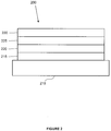
- FIG. 2 shows an inverted OLED 200.
- the device includes a substrate 210, a cathode 215, an emissive layer 220, a hole transport layer 225, and an anode 230.
- Device 200 may be fabricated by depositing the layers described, in order. Because the most common OLED configuration has a cathode disposed over the anode, and device 200 has cathode 215 disposed under anode 230, device 200 may be referred to as an "inverted" OLED. Materials similar to those described with respect to device 100 may be used in the corresponding layers of device 200.
- FIG. 2 provides one example of how some layers may be omitted from the structure of device 100.
- FIGS. 1 and 2 The simple layered structure illustrated in FIGS. 1 and 2 is provided by way of nonlimiting example, and it is understood that the method of the invention may be used in connection with a wide variety of other structures.
- the specific materials and structures described are exemplary in nature, and other materials and structures may be used.
- Functional OLEDs may be achieved by combining the various layers described in different ways, or layers may be omitted entirely, based on design, performance, and cost factors. Other layers not specifically described may also be included. Materials other than those specifically described may be used. Although many of the examples provided herein describe various layers as comprising a single material, it is understood that combinations of materials, such as a mixture of host and dopant, or more generally a mixture, may be used. Also, the layers may have various sublayers.
- hole transport layer 225 transports holes and injects holes into emissive layer 220, and may be described as a hole transport layer or a hole injection layer.
- an OLED may be described as having an "organic layer" disposed between a cathode and an anode. This organic layer may comprise a single layer, or may further comprise multiple layers of different organic materials as described, for example, with respect to FIGS. 1 and 2 .
- OLEDs comprised of polymeric materials (PLEDs) such as disclosed in U.S. Pat. No. 5,247,190 to Friend et al.
- PLEDs polymeric materials
- OLEDs having a single organic layer may be used.
- OLEDs may be stacked, for example as described in U.S. Pat. No. 5,707,745 to Forrest et al.
- the OLED structure may deviate from the simple layered structure illustrated in FIGS. 1 and 2 .
- the substrate may include an angled reflective surface to improve out-coupling, such as a mesa structure as described in U.S. Pat. No. 6,091,195 to Forrest et al. , and/or a pit structure as described in U.S. Pat. No. 5,834,893 to Bulovic et al.
- any of the layers of the various embodiments may be deposited by any suitable method.
- preferred methods include thermal evaporation, ink-jet, such as described in U.S. Pat. Nos. 6,013,982 and 6,087,196 , organic vapor phase deposition (OVPD), such as described in U.S. Pat. No. 6,337,102 to Forrest al. , and deposition by organic vapor jet printing (OVJP), such as described in U.S. patent application Ser. No. 10/233,470 .
- OVPD organic vapor phase deposition
- OJP organic vapor jet printing
- Other suitable deposition methods include spin coating and other solution based processes. Solution based processes are preferably carried out in nitrogen or an inert atmosphere.
- preferred methods include thermal evaporation.
- Preferred patterning methods include deposition through a mask, cold welding such as described in U.S. Pat. Nos. 6,294,398 and 6,468,819 . and patterning associated with some of the deposition methods such as ink-jet and OVJD. Other methods may also be used.
- the materials to be deposited may be modified to make them compatible with a particular deposition method.
- substituents such as alkyl and aryl groups, branched or unbranched, and preferably containing at least 3 carbons, may be used in small molecules to enhance their ability to undergo solution processing. Substituents having 20 carbons or more may be used, and 3-20 carbons is a preferred range. Materials with asymmetric structures may have better solution processibility than those having symmetric structures, because asymmetric materials may have a lower tendency to recrystallize. Dendrimer substituents may be used to enhance the ability of small molecules to undergo solution processing.
- Devices fabricated in accordance with the method of the invention may be incorporated into a wide variety of consumer products, including flat panel displays, computer monitors, televisions, billboards, lights for interior or exterior illumination and/or signaling, heads up displays, fully transparent displays, flexible displays, laser printers, telephones, cell phones, personal digital assistants (PDAs), laptop computers, digital cameras, camcorders, viewfinders, micro-displays, vehicles, a large area wall, theater or stadium screen, or a sign.
- PDAs personal digital assistants
- Various control mechanisms may be used to control devices fabricated in accordance with the present invention, including passive matrix and active matrix. Many of the devices are intended for use in a temperature range comfortable to humans, such as 18 degrees C. to 30 degrees C., and more preferably at room temperature (20-25 degrees C.).
- the materials and structures described herein may have applications in devices other than OLEDs.
- other optoelectronic devices such as organic solar cells and organic photodetectors may employ the materials and structures.
- organic devices such as organic transistors, may employ the materials and structures.
- a method according to claim 1 of fabricating an organic light emitting device is provided.
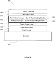
- Figure 3 shows an example of device 300 fabricated using the described method.
- the device is fabricated on a substrate 310.
- the device includes a first electrode 320, emitting layers 330 disposed over the first electrode 320, and a second electrode 340 disposed over the emitting layers 330.
- Emitting layers 330 include first organic layer 332 and second organic layer 334.
- First electrode 320 is preferably an anode and second electrode 340 is preferably a cathode, but other configurations may be used.
- First electrode 320 may be provided by any suitable method, including the purchase of commercially available substrates pre-coated with indium tin oxide (ITO) or other electrode material.
- First organic layer 332 is deposited via solution deposition over first electrode 320.
- the solution used to deposit first organic layer 332 includes a solvent, the organic host material of the first organic layer; the first organic emitting material of the first organic layer; and the second organic emitting material of the first organic layer. Other materials may be included.
- Second organic layer 334 is deposited by vapor deposition over and in direct contact with first organic layer 332.
- Second organic layer 334 includes an organic host and an organic emitting material of the second organic layer which are co-deposited.
- Second electrode 340 is subsequently deposited over second organic layer 334 by any suitable technique.
- Device 300 as illustrated also includes optional layers.
- a third organic layer 350 and a fourth organic layer 360 are disposed between emitting layers 330 and first electrode 320. Where first electrode 320 is an anode, third organic layer 350 may be a hole injection layer and fourth organic layer may be a hole transport layer.
- a fifth organic layer 370 is disposed between emitting layers 330 and second electrode 340. Where second electrode 340 is a cathode, fourth organic layer 370 may include a hole blocking layer, and an electron transport layer.
- Third, fourth and fifth organic layers 350, 360 and 370 may include sublayers, and may include other layers useful in various OLED architectures, many of which are described with respect to FIGS. 1 and 2 .
- the first organic emitting material of first organic layer 332 has a peak emissive wavelength in the visible spectrum of 590 - 700 nm
- the second organic emitting material of first organic layer 332 has a peak emissive wavelength in the visible spectrum at 500 - 590 nm
- the organic emitting material of second organic layer 334 has a peak emissive wavelength in the visible spectrum of 400 - 500 nm.
- peak wavelengths correspond roughly to red, green, and blue emitters, and are useful for obtaining a device that emits white light that would be useful, for example, for general illumination purposes.
- the first organic emitting material of first organic layer 332 is present in first organic layer 332 in a concentration of 0.01 - 5 wt %
- the second organic emitting material of first organic layer 332 is present in the first organic layer in a concentration that is 1.1 to 500 times the concentration of the concentration of the first organic emitting material.
- the second organic emitting material of first organic layer 332 is present in an amount not more than 40 wt%. Percentages are given as weight percentages of the organic layer after fabrication, and may generally be determined by using the relative weight percentages in solution of the various materials to be deposited, because the solvent evaporates.
- the first organic emitting material of first organic layer 332 is present in the in first organic layer 332 in a concentration of 0.2-4 wt%
- the second organic emitting material of first organic layer 332 is present in first organic layer 332 in a concentration that is 2 to 200 times the concentration of the concentration of the first organic emitting material.
- the second organic emitting material of first organic layer 332 is preferably present in an amount not more than 40 wt%.
- the first organic emitting material of first organic layer 332, the second organic emitting material of first organic layer 332, and the organic emitting material of second organic layer 334 are all small molecule materials.
- Many small molecule materials are suitable for solution deposition, or may be readily modified to render them suitable for solution deposition using known techniques involving the addition of bulky substituents.
- Second organic layer 334 comprises an organic host and the organic emitting material of second organic layer 334.
- Second organic 334 layer is deposited by vapor deposition, where the organic host of second organic layer 334 and the organic emitting material of second organic layer 334 are co-deposited.
- Vapor deposition includes vapor thermal evaporation (VTE), organic vapor phase deposition (OVPD), and organic vapor jet printing (OVJP). Vapor deposition is used because treatments to render underlying layers (such as first organic layer 332) insolvent often involve steps that would be detrimental to emitting materials.
- Third and fourth organic layers 350 and 360 when present, are preferably deposited via solution deposition techniques. Because these organic layers do not include emitting materials, material and processing choices are readily available that render these layers insoluble in a solvent used to deposit subsequent layers. One such process choice is baking to cross-link the material, rendering it insoluble.
- the organic light emitting device emits light having a CIE coordinate of x coordinate in the range of 0.15-0.65, and y coordinate in the range of 0.1-0.7. More preferably, the organic light emitting device emits light having a CIE coordinate of x coordinate in the range of 0.25 - 0.5, and y coordinate in the range of 0.2 - 0.5. These CIE coordinates are readily obtainable using the preferred peak wavelength choices for the emitting materials of the device.
- first organic layer 332 includes a small amount of red dopant, and a larger amount of green dopant.
- the amount of red dopant will generally be small, both in absolute terms and relative to the amount of green dopant. This is because when a red dopant is co-doped with a green dopant, excitons may preferentially move to the red dopant or transfer from the green dopant to the red dopant due to the lower energy of the red dopant.
- red dopant Due to this preferential emission from the red dopant, a significantly smaller amount of red and larger amount of green is needed than if the materials were in separate layers.
- amount of emission from red dopant relative to green dopant is highly sensitive to small variations in the concentrations of the dopants, again due to the preferential emission from the red dopant.
- Controlling the amount of dopant deposited via vapor deposition techniques such as VTE generally involves adjusting temperatures, aperture sizes and relative flow rates of materials.
- the variance in the amount of dopant deposited from run to run is typically about 5%. So if it were desired to deposit a layer having 1 wt% of red dopant, the actual amount of red dopant would be about 0.95 wt% to 1.05 wt%. Where the device includes a layer having co-doped red and green dopants (and the green dopant will also be expected to have a 5% variance), the variance is large enough to significantly alter the CIE coordinates of a device.
- controlling the amount of dopant for solution process techniques generally involves weighing the various materials and adding them to a solvent in carefully controlled amounts.
- a weight as low as 0.001 g of red dopant can be measured for use in solution using a micro balance with a precision of 0.00001 g (plus or minus).
- variance is 1%. This reduction in variance is expected to significantly improve the reproducibility of the CIE coordinates of the finished device.
- concentrations for a layer including only red and green dopants are about 1 wt% for the red dopant and about 12 wt% for the green dopant. Other combinations of dopants, and other concentrations may be used.
- a solution processed emitting layer may include three or more emitting materials.
- An example of this useful for a white-emitting device is a layer that includes 72 wt% host, 20 wt% green emitter, 5 wt% yellow and 3 wt% red.
- Another example is 68.9 wt% host, 30 wt% green, 1% red1, and 0.1% red2 where red1 and red2 are different red emitting materials.
- the first organic layer may further comprises a third organic emitting material of the first organic layer.
- a third organic dopant may be useful, for example, to add an additional emission color to fine tune the overall emission of the device, to adjust conductivity, or other uses.
- Emissive "dopants” may include phosphorescent emitting organic materials or fluorescent organic emitting materials.
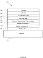
- Device 400 is a preferred specific structure of device 300.
- Device 400 is fabricated on a substrate 410, and includes, in order, anode 420, solution processed organic hole injection layer 452, solution processed organic hole transport layer 454, solution processed organic emissive layer 432, VTE deposited organic emissive layer 434, VTE deposited organic blocking layer 462, VTE deposited organic electron transport layer 464 and cathode 440.
- Solution processed organic emissive layer 432 includes a host and red and green emitting dopants
- VTE deposited organic emissive layer 434 includes a host and a blue emitting dopant.
- FIG. 5 shows a comparative example that does not include a solution deposited layer having multiple emissive dopants.
- Device 500 is fabricated on a substrate 510, and includes, in order, anode 520, VTE deposited organic hole injection layer 552, VTE deposited organic hole transport layer 554, VTE deposited organic emissive layer 532, VTE deposited organic emissive layer 534, VTE deposited organic blocking layer 562, VTE deposited organic electron transport layer 464 and cathode 440.
- VTE deposited organic emissive layer 532 includes a host and red and green emitting dopants
- VTE deposited organic emissive layer 534 includes a host and a blue emitting dopant.
- FIG. 6 shows a CIE diagram.
- the star is located at a target CIE coordinate that is desirable for white emission.
- the curve on which the star is located is the well-known blackbody radiation curve, which describes the color of thermal radiation from an object that absorbs all electromagnetic radiation that falls on it (a "black body”).
- FIG. 7 shows a target spectrum calculated using the emission spectra of the red, green and blue emitting materials of Example 1.
- LG101 and LG201 available for purchase from LG Chemical Corporation of Seoul, Korea.
- NS60 available for purchase from Nippon Steel Chemical Company of Tokyo, Japan.
- VTE vacuum thermal evaporation
- the color difference between different devices can be described by MacAdam Ellipses, which are a well-known measure of human ability to differentiate color.
- a MacAdam Ellipse is a region on a CIE diagram inside of which a particular number of humans can not differentiate between colors.
- 68% of people can perceive a color difference. 68% is the percentage that falls within one standard deviation on a bell curve.
- 95% of people can perceive a color difference, where 95% is the percentage that falls within two standard deviations on a bell curve, and so on.
- the lighting industry generally desires that the color of a light used for illumination be reproducible within a 3- or 4-step MacAdam ellipse. If color reproducibility is too low, a viewer looking at two sources of illumination would perceive significant differences. For example, the different panels of a ceiling light might appear to have different colors, or there might be a significantly perceivable variation within a panel, which is undesirable.
- FIG. 8 shows the CIE coordinates of the seven devices having the structure shown in FIG. 5 .
- FIG. 9 shows the same data as FIG. 8 , but the relevant region of the diagram is magnified.
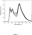
- FIG. 10 shows the measured spectra for the seven devices. It can be seen that there is a significant spread in the CIE coordinates of the different devices, and that they are all well outside of a 3-step MacAdam ellipse centered around the average of the CIE coordinates (0.424, 0.413) of the seven devices.
- the 7-step MacAdam ellipse can barely enclose the 7 device colors, which is out of industrial standard tolerance specification. This means that color reproducibility is not reliable for the VTE devices notwithstanding the care taken to achieve color reproducibility.
- the inventors attribute this variation in color to the sensitivity of the co-doped green and red emitting layer to the percentage of red dopant, and the relatively high variation in this percentage that occurs with a VTE deposition process.
- a device was fabricated having the structure shown in FIG 4 .
- the hole injecting material HIL-1 (as the host material) along with Conducting dopant-1 were dissolved in a cyclohexanone solution.
- the amount of Conducting dopant-1 in the solution was 10 wt% relative to the host material HIL-1.
- the total concentration of the HIL-1 and Conducting dopant-1 was 0.5wt% in cyclohexanone.
- HIL hole injection layer
- the solution was spin-coated at 4000 rpm for 60 seconds onto a patterned indium tin oxide (ITO) electrode.
- ITO indium tin oxide
- the resulting film was baked for 30 minutes at 250° C. The film became insoluble after baking.
- HTL hole transporting layer
- EML emitting layer
- the red and green EML was composed of a host material (Host-1) and a red and a green phosphorescent dopant (Red dopant-1 and Green dopant-1) as the emitting material.
- a toluene solution containing Host-1, Green dopant-1, and Red dopant (of total 0.75 wt%) with a Host-1 :Green dopant-1 :Red dopant-1 weight ratio of 87:12:1 was spin-coated onto the insoluble HTL at 1000 rpm for 60 seconds, and then baked at 100° C for 60 minutes.
- the blue EML was deposited using thermal evaporation.
- the 10 nm of blue host (Host-2) and Blue dopant-1 was co-evaporated with ratio of 90:10.
- On top of blue EML 5 nm neat Host-2 was evaporated to build blocking layer (BL).
- the electron transport layer (containing Alq3), the electron injection layer (containing LiF), and the aluminum electrode were sequentially vacuum deposited.
- the device of Example 2 had the structure: ITO (120 nm) / HIL-1:Conducting Dopant-1 (90:10; 5 nm) / HTL-1 (10 nm) / Host-1:Green Dopant-1:Red Dopant-1 (87:12:1; 25 nm) / Host-2:Blue Dopant-1: (90:10; 10 nm) / Host-2 (5 nm) / Alq 3 (40 nm) / LiF/Al
- the CIE coordinate and spectrum of the hybrid white device of Example 2 are shown in FIGS. 6 and 7 , respectively.
- the device performance is described in TABLE 1. At 1000 cd/m2, the power efficiency was 11 lm/W with color rendering index (CRI) 78, and correlated color temperature (CCT) corresponding to the white color was 2800K degree. Table 1.
- Example 2 Power Efficiency (lm/W) @ 1,000 cd/m2 11 Correlated Color Temperature (CCT) (K) @ 1,000 cd/m2 2800 Color Rendering Index (CRI) @ 1,000 cd/m2 78 Color Coordinate, CIE(x,y) @ 1,000 cd/m2 (0.453,0.411) Lifetime LT80 (hours) @ 4,000 cd/m2 (A brightness decay to 80% of initial level 4,000 cd/m2 100
Landscapes
- Engineering & Computer Science (AREA)
- Manufacturing & Machinery (AREA)
- Physics & Mathematics (AREA)
- Optics & Photonics (AREA)
- Electroluminescent Light Sources (AREA)
Claims (9)
- Verfahren zum Herstellen einer organischen lichtemittierenden Vorrichtung, umfassend:a. Bereitstellen einer ersten Elektrode;b. Depüonieren einer ersten organischen Schicht über der ersten Elektrode, wobei die erste organische Schicht ferner Folgendes umfasst:i. ein organisches Wirtsmaterial der ersten organischen Schicht;ii. ein erstes organisches emittierendes Material der ersten organischen Schicht;iii. ein zweites organisches emittierendes Material der ersten organischen Schicht;c. Deponieren einer zweiten organischen Schicht über der und in direktem Kontakt mit der ersten organischen Schicht, wobei die zweite organische Schicht ein organisches Wirtsmaterial und ein organisches emittierendes Material der zweiten organischen Schicht umfasst;d. Deponieren einer zweiten Elektrode über der zweiten organischen Schicht;wobei die zweite organische Schicht mittels Gasphasenabscheidung deponiert wird; und
wobei das organische Wirtsmaterial der zweiten organischen Schicht und das organische emittierende Material der zweiten organischen Schicht co-deponiert werden,
dadurch gekennzeichnet, dass die erste organische Schicht mittels Lösungsverarbeitung deponiert wird. - Verfahren nach Anspruch 1, wobei:a. das erste organische emittierende Material der ersten organischen Schicht eine Peakemissionswellenlänge im sichtbaren Spektrum von 590 bis 700 nm aufweist,b. das zweite organische emittierende Material der ersten organischen Schicht eine Peakemissionswellenlänge im sichtbaren Spektrum bei 500 bis 590 nm aufweist,c. das organische emittierende Material der zweiten organischen Schicht eine Peakemissionswellenlänge im sichtbaren Spektrum zwischen 400 und 500 nm aufweist.
- Verfahren nach Anspruch 2, wobei:das erste organische emittierende Material der ersten organischen Schicht in der ersten organischen Schicht in einer Konzentration von 0,01 bis 5 Gewichts-% vorliegt unddas zweite organische emittierende Material der ersten organischen Schicht in der ersten organischen Schicht in einer Konzentration vorliegt, die das 1,1- bis 500-Fache der Konzentration des ersten organischen emittierenden Materials und nicht mehr als 40 Gewichts-% beträgt.
- Verfahren nach Anspruch 2, wobei:das erste organische emittierende Material der ersten organischen Schicht in der ersten organischen Schicht in einer Konzentration von 0,2 bis 4 Gewichts-% vorliegt;das zweite organische emittierende Material der ersten organischen Schicht in der ersten organischen Schicht in einer Konzentration vorliegt, die das 2- bis 200-Fache der Konzentration des ersten organischen emittierenden Materials beträgt.
- Verfahren nach Anspruch 1, wobei sowohl das erste organische emittierende Material der ersten organischen Schicht als auch das zweite organische emittierende Material der ersten organischen Schicht als auch das organische emittierende Material der zweiten organischen Schicht kleinmolekulare Materialien sind.
- Verfahren nach Anspruch 1, ferner umfassend, vor dem Deponieren der ersten organischen Schicht:a. Deponieren einer dritten organischen Schicht, die ein organisches Material der dritten organischen Schicht umfasst, über der ersten Elektrode mittels Lösungsverarbeitung;b. Deponieren einer vierten organischen Schicht, die ein organisches Material der vierten organischen Schicht umfasst, über der dritten organischen Schicht mittels Lösungsverarbeitung,wobei die dritte organische Schicht sich nicht auflöst, wenn die vierte organische Schicht deponiert wird, und sich die vierte organische Schicht nicht auflöst, wenn die erste organische Schicht deponiert wird.
- Verfahren nach Anspruch 1, wobei die organische lichtemittierende Vorrichtung Licht mit einer x-Koordinate im CIE-System im Bereich zwischen 0,15 und 0,65 und einer y-Koordinate im Bereich zwischen 0,1 und 0,7 emittiert.
- Verfahren nach Anspruch 7, wobei die organische lichtemittierende Vorrichtung Licht mit einer x-Koordinate im CIE-System im Bereich zwischen 0,25 und 0,5 und einer y-Koordinate im Bereich zwischen 0,2 und 0,5 emittiert.
- Verfahren nach Anspruch 1, wobei die erste organische Schicht ferner ein drittes organisches emittierendes Material der ersten organischen Schicht umfasst.
Applications Claiming Priority (3)
| Application Number | Priority Date | Filing Date | Title |
|---|---|---|---|
| US29668010P | 2010-01-20 | 2010-01-20 | |
| US12/913,443 US8288187B2 (en) | 2010-01-20 | 2010-10-27 | Electroluminescent devices for lighting applications |
| PCT/US2010/056021 WO2011090535A1 (en) | 2010-01-20 | 2010-11-09 | Electroluminescent devices for lighting applications |
Publications (2)
| Publication Number | Publication Date |
|---|---|
| EP2526577A1 EP2526577A1 (de) | 2012-11-28 |
| EP2526577B1 true EP2526577B1 (de) | 2020-03-25 |
Family
ID=44277870
Family Applications (1)
| Application Number | Title | Priority Date | Filing Date |
|---|---|---|---|
| EP10778807.7A Active EP2526577B1 (de) | 2010-01-20 | 2010-11-09 | Elektrolumineszenzbauelemente für beleuchtungsanwendungen |
Country Status (7)
| Country | Link |
|---|---|
| US (3) | US8288187B2 (de) |
| EP (1) | EP2526577B1 (de) |
| JP (3) | JP5642805B2 (de) |
| KR (2) | KR20170021376A (de) |
| CN (2) | CN102792480B (de) |
| TW (2) | TWI524569B (de) |
| WO (1) | WO2011090535A1 (de) |
Families Citing this family (40)
| Publication number | Priority date | Publication date | Assignee | Title |
|---|---|---|---|---|
| US8288187B2 (en) * | 2010-01-20 | 2012-10-16 | Universal Display Corporation | Electroluminescent devices for lighting applications |
| TW201221597A (en) * | 2010-11-03 | 2012-06-01 | Cambrios Technologies Corp | Coating compositions for forming nanocomposite films |
| KR102012047B1 (ko) | 2012-01-06 | 2019-08-19 | 유니버셜 디스플레이 코포레이션 | 효율이 큰 인광 물질 |
| WO2013180539A1 (ko) * | 2012-05-31 | 2013-12-05 | 주식회사 엘지화학 | 유기전계발광소자 |
| WO2014044722A1 (en) | 2012-09-20 | 2014-03-27 | Basf Se | Azadibenzofurans for electronic applications |
| GB2509718A (en) * | 2013-01-09 | 2014-07-16 | Cambridge Display Tech Ltd | Method for forming a layer of an electronic device and appropriate precursor compounds |
| US8809848B1 (en) * | 2013-03-07 | 2014-08-19 | National Tsing Hua University | Full-band and high-CRI organic light-emitting diode |
| US10074806B2 (en) | 2013-08-20 | 2018-09-11 | Universal Display Corporation | Organic electroluminescent materials and devices |
| US9385348B2 (en) | 2013-08-29 | 2016-07-05 | The Regents Of The University Of Michigan | Organic electronic devices with multiple solution-processed layers |
| JP2016529730A (ja) | 2013-08-29 | 2016-09-23 | ザ・リージェンツ・オブ・ザ・ユニバーシティ・オブ・ミシガン | 多数の溶液処理層を有する有機電子デバイス |
| EP3063153B1 (de) | 2013-10-31 | 2018-03-07 | Idemitsu Kosan Co., Ltd. | Azadibenzothiophene für electronische anwendungen |
| JP6675304B2 (ja) * | 2014-04-25 | 2020-04-01 | 住友化学株式会社 | 発光素子 |
| JP2014220248A (ja) * | 2014-06-25 | 2014-11-20 | 三菱化学株式会社 | 有機電界発光素子の製造方法 |
| WO2016016791A1 (en) | 2014-07-28 | 2016-02-04 | Idemitsu Kosan Co., Ltd (Ikc) | 2,9-functionalized benzimidazolo[1,2-a]benzimidazoles as hosts for organic light emitting diodes (oleds) |
| EP2982676B1 (de) | 2014-08-07 | 2018-04-11 | Idemitsu Kosan Co., Ltd. | Benzimidazo[2,1-b]benzoxazole für elektronische Anwendungen |
| TWI663173B (zh) | 2014-08-08 | 2019-06-21 | 愛爾蘭商Udc愛爾蘭責任有限公司 | 電致發光咪唑并喹噁啉碳烯金屬錯合物 |
| EP2993215B1 (de) | 2014-09-04 | 2019-06-19 | Idemitsu Kosan Co., Ltd. | Azabenzimidazo[2,1-a]benzimidazole für elektronische Anwendungen |
| EP3015469B1 (de) | 2014-10-30 | 2018-12-19 | Idemitsu Kosan Co., Ltd. | 5-(benzimidazol-2-yl)benzimidazo[1,2-a]benzimidazole für elektronische Anwendungen |
| WO2016079667A1 (en) | 2014-11-17 | 2016-05-26 | Idemitsu Kosan Co., Ltd. | Indole derivatives for electronic applications |
| WO2016079169A1 (en) | 2014-11-18 | 2016-05-26 | Basf Se | Pt- or pd-carbene complexes for use in organic light emitting diodes |
| EP3034506A1 (de) | 2014-12-15 | 2016-06-22 | Idemitsu Kosan Co., Ltd | 4-funktionalisierte Carbazolderivate für elektronische Anwendungen |
| EP3034507A1 (de) | 2014-12-15 | 2016-06-22 | Idemitsu Kosan Co., Ltd | 1-funktionalisierte Dibenzofurane und Dibenzothiophene für organische Leuchtdioden (OLEDS) |
| US20180022990A1 (en) * | 2015-02-03 | 2018-01-25 | Sumitomo Chemical Company, Limited | Composition and light emitting device using the same |
| EP3054498B1 (de) | 2015-02-06 | 2017-09-20 | Idemitsu Kosan Co., Ltd. | Bisimidazodiazozine |
| EP3053918B1 (de) | 2015-02-06 | 2018-04-11 | Idemitsu Kosan Co., Ltd. | 2-Carbazol substituierte Benzimidazole für Elektronische Anwendungen |
| EP3061759B1 (de) | 2015-02-24 | 2019-12-25 | Idemitsu Kosan Co., Ltd | Nitrilsubstituierte dibenzofurane |
| EP3070144B1 (de) | 2015-03-17 | 2018-02-28 | Idemitsu Kosan Co., Ltd. | Siebengliedrige ringverbindungen |
| EP3072943B1 (de) | 2015-03-26 | 2018-05-02 | Idemitsu Kosan Co., Ltd. | Dibenzofuran/carbazol-substituierte benzonitrile |
| EP3075737B1 (de) | 2015-03-31 | 2019-12-04 | Idemitsu Kosan Co., Ltd | Benzimidazolo[1,2-a]benzimidazol mit aryl- oder heteroarylnitrilgruppen für organische leuchtdioden |
| EP3356369B1 (de) | 2015-10-01 | 2022-05-04 | Idemitsu Kosan Co., Ltd | Triazingruppen tragende benzimidazolo[1,2-a]benzimidazol für organische leuchtdioden |
| EP3150604B1 (de) | 2015-10-01 | 2021-07-14 | Idemitsu Kosan Co., Ltd. | Benzimidazolo[1,2-a]benzimidazol mit benzimidazolo[1,2-a]benzimidazolylgruppen, carbazolylgruppen, benzofurangruppen oder benzothiophengruppen für organische leuchtdioden |
| WO2017056053A1 (en) | 2015-10-01 | 2017-04-06 | Idemitsu Kosan Co., Ltd. | Benzimidazolo[1,2-a]benzimidazole carrying benzimidazolo[1,2-a]benzimidazolyl groups, carbazolyl groups, benzofurane groups or benzothiophene groups for organic light emitting diodes |
| EP3150606B1 (de) | 2015-10-01 | 2019-08-14 | Idemitsu Kosan Co., Ltd. | Benzimidazolo[1,2-a]benzimidazoles mit benzofuran-oder benzothiophen gruppen für organische licht emittierende dioden |
| KR20180079328A (ko) | 2015-11-04 | 2018-07-10 | 이데미쓰 고산 가부시키가이샤 | 벤즈이미다졸 축합 헤테로아릴 |
| WO2017093958A1 (en) | 2015-12-04 | 2017-06-08 | Idemitsu Kosan Co., Ltd. | Benzimidazolo[1,2-a]benzimidazole derivatives for organic light emitting diodes |
| KR102684614B1 (ko) | 2015-12-21 | 2024-07-15 | 유디씨 아일랜드 리미티드 | 삼각형 리간드를 갖는 전이 금속 착체 및 oled에서의 이의 용도 |
| KR102553276B1 (ko) * | 2016-03-29 | 2023-07-06 | 엘지디스플레이 주식회사 | 유기발광 표시장치 |
| US10968229B2 (en) | 2016-04-12 | 2021-04-06 | Idemitsu Kosan Co., Ltd. | Seven-membered ring compounds |
| JP6151846B1 (ja) * | 2016-12-27 | 2017-06-21 | Lumiotec株式会社 | 有機エレクトロルミネッセント素子、照明装置、ディスプレイ装置 |
| US10770673B2 (en) * | 2017-11-28 | 2020-09-08 | The Regents Of The University Of Michigan | Highly reliable stacked white organic light emitting device |
Family Cites Families (254)
| Publication number | Priority date | Publication date | Assignee | Title |
|---|---|---|---|---|
| DE20221915U1 (de) | 1977-06-01 | 2009-06-04 | Idemitsu Kosan Co. Ltd. | Organische Elektrolumineszenzvorrichtung |
| US4769292A (en) | 1987-03-02 | 1988-09-06 | Eastman Kodak Company | Electroluminescent device with modified thin film luminescent zone |
| GB8909011D0 (en) | 1989-04-20 | 1989-06-07 | Friend Richard H | Electroluminescent devices |
| US5061569A (en) | 1990-07-26 | 1991-10-29 | Eastman Kodak Company | Electroluminescent device with organic electroluminescent medium |
| DE69129907T2 (de) | 1990-11-30 | 1998-12-10 | Idemitsu Kosan Co. Ltd., Tokio/Tokyo | Organische elektroluminszente vorrichtung |
| DE4325885A1 (de) | 1993-08-02 | 1995-02-09 | Basf Ag | Elektrolumineszierende Anordnung |
| DE69412567T2 (de) | 1993-11-01 | 1999-02-04 | Hodogaya Chemical Co., Ltd., Tokio/Tokyo | Aminverbindung und sie enthaltende Elektrolumineszenzvorrichtung |
| US5503910A (en) | 1994-03-29 | 1996-04-02 | Idemitsu Kosan Co., Ltd. | Organic electroluminescence device |
| US5424560A (en) | 1994-05-31 | 1995-06-13 | Motorola, Inc. | Integrated multicolor organic led array |
| US5703436A (en) | 1994-12-13 | 1997-12-30 | The Trustees Of Princeton University | Transparent contacts for organic devices |
| US5707745A (en) | 1994-12-13 | 1998-01-13 | The Trustees Of Princeton University | Multicolor organic light emitting devices |
| DE19500912A1 (de) | 1995-01-13 | 1996-07-18 | Basf Ag | Elektrolumineszierende Anordnung |
| US5693428A (en) | 1995-02-06 | 1997-12-02 | Sanyo Electric Co., Ltd. | Organic electroluminescent device |
| US5552253A (en) | 1995-03-31 | 1996-09-03 | Xerox Corporation | Multiple layer photoreceptor for color xerography |
| JP4477150B2 (ja) | 1996-01-17 | 2010-06-09 | 三星モバイルディスプレイ株式會社 | 有機薄膜el素子 |
| US5929194A (en) | 1996-02-23 | 1999-07-27 | The Dow Chemical Company | Crosslinkable or chain extendable polyarylpolyamines and films thereof |
| US6939625B2 (en) | 1996-06-25 | 2005-09-06 | Nôrthwestern University | Organic light-emitting diodes and methods for assembly and enhanced charge injection |
| US5844363A (en) | 1997-01-23 | 1998-12-01 | The Trustees Of Princeton Univ. | Vacuum deposited, non-polymeric flexible organic light emitting devices |
| JP3899566B2 (ja) | 1996-11-25 | 2007-03-28 | セイコーエプソン株式会社 | 有機el表示装置の製造方法 |
| JPH10162955A (ja) | 1996-11-28 | 1998-06-19 | Seiko Precision Kk | 有機el素子の製造方法 |
| US5834893A (en) | 1996-12-23 | 1998-11-10 | The Trustees Of Princeton University | High efficiency organic light emitting devices with light directing structures |
| US6091195A (en) | 1997-02-03 | 2000-07-18 | The Trustees Of Princeton University | Displays having mesa pixel configuration |
| US6013982A (en) | 1996-12-23 | 2000-01-11 | The Trustees Of Princeton University | Multicolor display devices |
| US6130001A (en) | 1997-07-15 | 2000-10-10 | Motorola, Inc. | Organic electroluminescent device with continuous organic medium |
| JP3861400B2 (ja) | 1997-09-01 | 2006-12-20 | セイコーエプソン株式会社 | 電界発光素子およびその製造方法 |
| WO1999012395A1 (en) | 1997-09-02 | 1999-03-11 | Seiko Epson Corporation | Method of producing organic el element and organic el element |
| US5853905A (en) | 1997-09-08 | 1998-12-29 | Motorola, Inc. | Efficient single layer electroluminescent device |
| US6303238B1 (en) | 1997-12-01 | 2001-10-16 | The Trustees Of Princeton University | OLEDs doped with phosphorescent compounds |
| US6592933B2 (en) | 1997-10-15 | 2003-07-15 | Toray Industries, Inc. | Process for manufacturing organic electroluminescent device |
| JP4963754B2 (ja) | 1997-10-23 | 2012-06-27 | イシス イノベイション リミテッド | 光放射デンドリマー及び光放射装置 |
| US5851709A (en) | 1997-10-31 | 1998-12-22 | Eastman Kodak Company | Method for selective transfer of a color organic layer |
| US6337102B1 (en) * | 1997-11-17 | 2002-01-08 | The Trustees Of Princeton University | Low pressure vapor phase deposition of organic thin films |
| US6087196A (en) | 1998-01-30 | 2000-07-11 | The Trustees Of Princeton University | Fabrication of organic semiconductor devices using ink jet printing |
| JPH11273859A (ja) | 1998-03-24 | 1999-10-08 | Sony Corp | 有機電界発光素子及びその製造方法 |
| GB2335884A (en) | 1998-04-02 | 1999-10-06 | Cambridge Display Tech Ltd | Flexible substrates for electronic or optoelectronic devices |
| ES2359884T3 (es) * | 1998-07-08 | 2011-05-27 | Toyota Jidosha Kabushiki Kaisha | Aparato para la reforma de combustibles. |
| JP2000036386A (ja) | 1998-07-16 | 2000-02-02 | Alps Electric Co Ltd | 白色発光エレクトロルミネッセンス素子 |
| US6528187B1 (en) | 1998-09-08 | 2003-03-04 | Fuji Photo Film Co., Ltd. | Material for luminescence element and luminescence element using the same |
| US6097147A (en) | 1998-09-14 | 2000-08-01 | The Trustees Of Princeton University | Structure for high efficiency electroluminescent device |
| US6830828B2 (en) | 1998-09-14 | 2004-12-14 | The Trustees Of Princeton University | Organometallic complexes as phosphorescent emitters in organic LEDs |
| US6107452A (en) | 1998-10-09 | 2000-08-22 | International Business Machines Corporation | Thermally and/or photochemically crosslinked electroactive polymers in the manufacture of opto-electronic devices |
| JP3287344B2 (ja) | 1998-10-09 | 2002-06-04 | 株式会社デンソー | 有機el素子 |
| US6221438B1 (en) | 1998-11-03 | 2001-04-24 | Sarnoff Corporation | Patterned deposition of a material |
| US6228436B1 (en) | 1998-12-16 | 2001-05-08 | Battelle Memorial Institute | Method of making light emitting polymer composite material |
| US6066357A (en) | 1998-12-21 | 2000-05-23 | Eastman Kodak Company | Methods of making a full-color organic light-emitting display |
| JP3900724B2 (ja) | 1999-01-11 | 2007-04-04 | セイコーエプソン株式会社 | 有機el素子の製造方法および有機el表示装置 |
| GB9903251D0 (en) | 1999-02-12 | 1999-04-07 | Cambridge Display Tech Ltd | Opto-electric devices |
| GB2347013A (en) | 1999-02-16 | 2000-08-23 | Sharp Kk | Charge-transport structures |
| US6294398B1 (en) | 1999-11-23 | 2001-09-25 | The Trustees Of Princeton University | Method for patterning devices |
| US6458475B1 (en) | 1999-11-24 | 2002-10-01 | The Trustee Of Princeton University | Organic light emitting diode having a blue phosphorescent molecule as an emitter |
| JP4477726B2 (ja) | 1999-12-09 | 2010-06-09 | シャープ株式会社 | 有機led素子の製造方法 |
| US6372154B1 (en) | 1999-12-30 | 2002-04-16 | Canon Kabushiki Kaisha | Luminescent ink for printing of organic luminescent devices |
| KR100377321B1 (ko) | 1999-12-31 | 2003-03-26 | 주식회사 엘지화학 | 피-형 반도체 성질을 갖는 유기 화합물을 포함하는 전기소자 |
| US6565994B2 (en) | 2000-02-10 | 2003-05-20 | Fuji Photo Film Co., Ltd. | Light emitting device material comprising iridium complex and light emitting device using same material |
| TW532048B (en) | 2000-03-27 | 2003-05-11 | Idemitsu Kosan Co | Organic electroluminescence element |
| TW512646B (en) | 2000-03-31 | 2002-12-01 | Seiko Epson Corp | Organic EL device and production method thereof |
| GB0013394D0 (en) | 2000-06-01 | 2000-07-26 | Microemissive Displays Ltd | A method of creating a color optoelectronic device |
| US20020121638A1 (en) | 2000-06-30 | 2002-09-05 | Vladimir Grushin | Electroluminescent iridium compounds with fluorinated phenylpyridines, phenylpyrimidines, and phenylquinolines and devices made with such compounds |
| CN101924190B (zh) | 2000-08-11 | 2012-07-04 | 普林斯顿大学理事会 | 有机金属化合物和发射转换有机电致磷光 |
| JP4040249B2 (ja) | 2000-11-16 | 2008-01-30 | 富士フイルム株式会社 | 発光素子 |
| JP2002175887A (ja) | 2000-12-07 | 2002-06-21 | Denso Corp | 有機el素子 |
| US6579630B2 (en) | 2000-12-07 | 2003-06-17 | Canon Kabushiki Kaisha | Deuterated semiconducting organic compounds used for opto-electronic devices |
| US6803720B2 (en) | 2000-12-15 | 2004-10-12 | Universal Display Corporation | Highly stable and efficient OLEDs with a phosphorescent-doped mixed layer architecture |
| TW518909B (en) | 2001-01-17 | 2003-01-21 | Semiconductor Energy Lab | Luminescent device and method of manufacturing same |
| JP3812730B2 (ja) | 2001-02-01 | 2006-08-23 | 富士写真フイルム株式会社 | 遷移金属錯体及び発光素子 |
| JP4307000B2 (ja) | 2001-03-08 | 2009-08-05 | キヤノン株式会社 | 金属配位化合物、電界発光素子及び表示装置 |
| AU2002306698A1 (en) | 2001-03-14 | 2002-09-24 | The Trustees Of Princeton University | Materials and devices for blue phosphorescence based organic light emitting diodes |
| KR100888424B1 (ko) | 2001-05-16 | 2009-03-11 | 더 트러스티즈 오브 프린스턴 유니버시티 | 고효율 다칼라 전기 유기 발광 장치 |
| JP4310077B2 (ja) | 2001-06-19 | 2009-08-05 | キヤノン株式会社 | 金属配位化合物及び有機発光素子 |
| AU2002345362A1 (en) | 2001-06-20 | 2003-01-08 | Showa Denko K.K. | Light emitting material and organic light-emitting device |
| US6699597B2 (en) | 2001-08-16 | 2004-03-02 | 3M Innovative Properties Company | Method and materials for patterning of an amorphous, non-polymeric, organic matrix with electrically active material disposed therein |
| US7071615B2 (en) | 2001-08-20 | 2006-07-04 | Universal Display Corporation | Transparent electrodes |
| JP4409942B2 (ja) | 2001-08-29 | 2010-02-03 | ザ トラスティーズ オブ プリンストン ユニバーシテイ | 金属錯体を含むキャリア輸送層を有する有機発光デバイス |
| EP1421827B1 (de) | 2001-08-29 | 2012-02-22 | The Trustees Of Princeton University | Organische lichtemittierende einrichtungen mit trägerblockierschichten mit metallkomplexen |
| US7250226B2 (en) | 2001-08-31 | 2007-07-31 | Nippon Hoso Kyokai | Phosphorescent compound, a phosphorescent composition and an organic light-emitting device |
| US7431968B1 (en) | 2001-09-04 | 2008-10-07 | The Trustees Of Princeton University | Process and apparatus for organic vapor jet deposition |
| US6835469B2 (en) | 2001-10-17 | 2004-12-28 | The University Of Southern California | Phosphorescent compounds and devices comprising the same |
| US7166368B2 (en) | 2001-11-07 | 2007-01-23 | E. I. Du Pont De Nemours And Company | Electroluminescent platinum compounds and devices made with such compounds |
| US6869695B2 (en) | 2001-12-28 | 2005-03-22 | The Trustees Of Princeton University | White light emitting OLEDs from combined monomer and aggregate emission |
| US6863997B2 (en) | 2001-12-28 | 2005-03-08 | The Trustees Of Princeton University | White light emitting OLEDs from combined monomer and aggregate emission |
| KR100691543B1 (ko) | 2002-01-18 | 2007-03-09 | 주식회사 엘지화학 | 새로운 전자 수송용 물질 및 이를 이용한 유기 발광 소자 |
| JP3786023B2 (ja) | 2002-01-31 | 2006-06-14 | 株式会社豊田自動織機 | 有機el素子 |
| JP3933591B2 (ja) * | 2002-03-26 | 2007-06-20 | 淳二 城戸 | 有機エレクトロルミネッセント素子 |
| US6951694B2 (en) | 2002-03-29 | 2005-10-04 | The University Of Southern California | Organic light emitting devices with electron blocking layers |
| JP3919583B2 (ja) | 2002-04-12 | 2007-05-30 | キヤノン株式会社 | 有機発光素子 |
| US6946677B2 (en) | 2002-06-14 | 2005-09-20 | Nokia Corporation | Pre-patterned substrate for organic thin film transistor structures and circuits and related method for making same |
| US20030230980A1 (en) | 2002-06-18 | 2003-12-18 | Forrest Stephen R | Very low voltage, high efficiency phosphorescent oled in a p-i-n structure |
| KR100480442B1 (ko) * | 2002-08-17 | 2005-04-06 | 한국과학기술연구원 | 미량도핑에 의한 고효율 백색 유기 발광 물질 및 이를이용한 전기발광소자 |
| US7189989B2 (en) | 2002-08-22 | 2007-03-13 | Fuji Photo Film Co., Ltd. | Light emitting element |
| DE10238903A1 (de) | 2002-08-24 | 2004-03-04 | Covion Organic Semiconductors Gmbh | Rhodium- und Iridium-Komplexe |
| JP4313308B2 (ja) | 2002-08-27 | 2009-08-12 | 富士フイルム株式会社 | 有機金属錯体、有機el素子及び有機elディスプレイ |
| US7098060B2 (en) | 2002-09-06 | 2006-08-29 | E.I. Du Pont De Nemours And Company | Methods for producing full-color organic electroluminescent devices |
| US6687266B1 (en) | 2002-11-08 | 2004-02-03 | Universal Display Corporation | Organic light emitting materials and devices |
| US6982179B2 (en) * | 2002-11-15 | 2006-01-03 | University Display Corporation | Structure and method of fabricating organic devices |
| US20040096570A1 (en) | 2002-11-15 | 2004-05-20 | Michael Weaver | Structure and method of fabricating organic devices |
| US6891326B2 (en) | 2002-11-15 | 2005-05-10 | Universal Display Corporation | Structure and method of fabricating organic devices |
| EP2248870B1 (de) | 2002-11-26 | 2018-12-26 | Konica Minolta Holdings, Inc. | Organisches Elektrolumineszenzelement und Anzeige- und Beleuchtungsvorrichtung |
| WO2004060026A1 (ja) | 2002-12-26 | 2004-07-15 | Semiconductor Energy Laboratory Co., Ltd. | 有機発光素子 |
| JP4365196B2 (ja) | 2002-12-27 | 2009-11-18 | 富士フイルム株式会社 | 有機電界発光素子 |
| JP4365199B2 (ja) | 2002-12-27 | 2009-11-18 | 富士フイルム株式会社 | 有機電界発光素子 |
| WO2004066685A1 (ja) | 2003-01-24 | 2004-08-05 | Idemitsu Kosan Co., Ltd. | 有機エレクトロルミネッセンス素子 |
| EP3109238B1 (de) | 2003-03-24 | 2019-09-18 | University of Southern California | Phenyl-pyrazol-komplexe des iridiums |
| JP3970253B2 (ja) | 2003-03-27 | 2007-09-05 | 三洋電機株式会社 | 有機エレクトロルミネッセンス素子 |
| US7090928B2 (en) | 2003-04-01 | 2006-08-15 | The University Of Southern California | Binuclear compounds |
| US7862906B2 (en) | 2003-04-09 | 2011-01-04 | Semiconductor Energy Laboratory Co., Ltd. | Electroluminescent element and light-emitting device |
| US7345301B2 (en) | 2003-04-15 | 2008-03-18 | Merck Patent Gmbh | Mixtures of matrix materials and organic semiconductors capable of emission, use of the same and electronic components containing said mixtures |
| US7029765B2 (en) | 2003-04-22 | 2006-04-18 | Universal Display Corporation | Organic light emitting devices having reduced pixel shrinkage |
| JP4635870B2 (ja) | 2003-04-23 | 2011-02-23 | コニカミノルタホールディングス株式会社 | 有機エレクトロルミネッセンス素子、照明装置及び表示装置 |
| CN100483779C (zh) | 2003-05-29 | 2009-04-29 | 新日铁化学株式会社 | 有机电致发光元件 |
| WO2004108857A1 (en) | 2003-06-02 | 2004-12-16 | Fuji Photo Film Co., Ltd. | Organic electroluminescent devices and metal complex compounds |
| TW200504175A (en) | 2003-06-09 | 2005-02-01 | Hitachi Chemical Co Ltd | Metal coordination compound, polymer composition and organic electroluminescence element using the same |
| JP2005011610A (ja) | 2003-06-18 | 2005-01-13 | Nippon Steel Chem Co Ltd | 有機電界発光素子 |
| JP4899284B2 (ja) | 2003-07-18 | 2012-03-21 | コニカミノルタホールディングス株式会社 | 有機エレクトロルミネッセンス素子、照明装置及び表示装置 |
| US20050025993A1 (en) | 2003-07-25 | 2005-02-03 | Thompson Mark E. | Materials and structures for enhancing the performance of organic light emitting devices |
| TWI390006B (zh) | 2003-08-07 | 2013-03-21 | Nippon Steel Chemical Co | Organic EL materials with aluminum clamps |
| DE10338550A1 (de) | 2003-08-19 | 2005-03-31 | Basf Ag | Übergangsmetallkomplexe mit Carbenliganden als Emitter für organische Licht-emittierende Dioden (OLEDs) |
| US7504049B2 (en) | 2003-08-25 | 2009-03-17 | Semiconductor Energy Laboratory Co., Ltd. | Electrode device for organic device, electronic device having electrode device for organic device, and method of forming electrode device for organic device |
| KR100560783B1 (ko) | 2003-09-03 | 2006-03-13 | 삼성에스디아이 주식회사 | 도핑된 발광층을 갖는 유기전계발광소자 |
| HU0302888D0 (en) | 2003-09-09 | 2003-11-28 | Pribenszky Csaba Dr | In creasing of efficacity of stable storage by freezing of embryos in preimplantation stage with pretreatment by pressure |
| US20060269780A1 (en) | 2003-09-25 | 2006-11-30 | Takayuki Fukumatsu | Organic electroluminescent device |
| EP1683804B1 (de) | 2003-11-04 | 2013-07-31 | Takasago International Corporation | Platinkomplex und lumineszentes element |
| JP4822687B2 (ja) | 2003-11-21 | 2011-11-24 | 富士フイルム株式会社 | 有機電界発光素子 |
| US7151339B2 (en) | 2004-01-30 | 2006-12-19 | Universal Display Corporation | OLED efficiency by utilization of different doping concentrations within the device emissive layer |
| US7332232B2 (en) | 2004-02-03 | 2008-02-19 | Universal Display Corporation | OLEDs utilizing multidentate ligand systems |
| KR100882172B1 (ko) | 2004-03-11 | 2009-02-06 | 미쓰비시 가가꾸 가부시키가이샤 | 전하 수송막용 조성물 및 이온 화합물, 이를 이용한 전하수송막 및 유기 전계 발광 장치, 및 유기 전계 발광 장치의제조 방법 및 전하 수송막의 제조 방법 |
| TW200531592A (en) | 2004-03-15 | 2005-09-16 | Nippon Steel Chemical Co | Organic electroluminescent device |
| TWI252051B (en) | 2004-03-31 | 2006-03-21 | Fujitsu Ltd | Organic electroluminescent device and organic electroluminescent display device |
| JP4869565B2 (ja) | 2004-04-23 | 2012-02-08 | 富士フイルム株式会社 | 有機電界発光素子 |
| US7655323B2 (en) | 2004-05-18 | 2010-02-02 | The University Of Southern California | OLEDs utilizing macrocyclic ligand systems |
| US7154114B2 (en) | 2004-05-18 | 2006-12-26 | Universal Display Corporation | Cyclometallated iridium carbene complexes for use as hosts |
| US7534505B2 (en) | 2004-05-18 | 2009-05-19 | The University Of Southern California | Organometallic compounds for use in electroluminescent devices |
| US7445855B2 (en) | 2004-05-18 | 2008-11-04 | The University Of Southern California | Cationic metal-carbene complexes |
| US7279704B2 (en) | 2004-05-18 | 2007-10-09 | The University Of Southern California | Complexes with tridentate ligands |
| US7393599B2 (en) | 2004-05-18 | 2008-07-01 | The University Of Southern California | Luminescent compounds with carbene ligands |
| US7491823B2 (en) | 2004-05-18 | 2009-02-17 | The University Of Southern California | Luminescent compounds with carbene ligands |
| JP4631316B2 (ja) | 2004-06-07 | 2011-02-16 | パナソニック株式会社 | エレクトロルミネセンス素子 |
| WO2005123873A1 (ja) | 2004-06-17 | 2005-12-29 | Konica Minolta Holdings, Inc. | 有機エレクトロルミネッセンス素子材料、有機エレクトロルミネッセンス素子、表示装置及び照明装置 |
| WO2006000544A2 (en) | 2004-06-28 | 2006-01-05 | Ciba Specialty Chemicals Holding Inc. | Electroluminescent metal complexes with triazoles and benzotriazoles |
| US20060008670A1 (en) | 2004-07-06 | 2006-01-12 | Chun Lin | Organic light emitting materials and devices |
| EP2178348B1 (de) | 2004-07-23 | 2012-11-21 | Konica Minolta Holdings, Inc. | Organisches elektrolumineszentes Element, Bildschirm und Beleuchtungseinheit |
| JP4110160B2 (ja) | 2004-09-29 | 2008-07-02 | キヤノン株式会社 | 有機エレクトロルミネッセント素子、及びディスプレイ装置 |
| DE102004057072A1 (de) | 2004-11-25 | 2006-06-01 | Basf Ag | Verwendung von Übergangsmetall-Carbenkomplexen in organischen Licht-emittierenden Dioden (OLEDs) |
| JP4496949B2 (ja) | 2004-12-13 | 2010-07-07 | 株式会社豊田自動織機 | 有機el素子 |
| ATE430789T1 (de) | 2004-12-23 | 2009-05-15 | Ciba Holding Inc | Elektrolumineszierende metallkomplexe mit nukleophilen carbenliganden |
| US7230107B1 (en) | 2004-12-29 | 2007-06-12 | E. I. Du Pont De Nemours And Company | Metal quinoline complexes |
| US8362463B2 (en) | 2004-12-30 | 2013-01-29 | E. I. Du Pont De Nemours And Company | Organometallic complexes |
| JPWO2006082742A1 (ja) | 2005-02-04 | 2008-06-26 | コニカミノルタホールディングス株式会社 | 有機エレクトロルミネッセンス素子材料、有機エレクトロルミネッセンス素子、表示装置及び照明装置 |
| KR100787428B1 (ko) * | 2005-03-05 | 2007-12-26 | 삼성에스디아이 주식회사 | 유기 전계 발광 소자 |
| KR100803125B1 (ko) | 2005-03-08 | 2008-02-14 | 엘지전자 주식회사 | 적색 인광 화합물 및 이를 사용한 유기전계발광소자 |
| JP5125502B2 (ja) | 2005-03-16 | 2013-01-23 | コニカミノルタホールディングス株式会社 | 有機エレクトロルミネッセンス素子材料、有機エレクトロルミネッセンス素子 |
| TWI293234B (en) * | 2005-03-24 | 2008-02-01 | Nat Univ Tsing Hua | White organic light-emitting diode and fabrication method |
| DE102005014284A1 (de) | 2005-03-24 | 2006-09-28 | Basf Ag | Verwendung von Verbindungen, welche aromatische oder heteroaromatische über Carbonyl-Gruppen enthaltende Gruppen verbundene Ringe enthalten, als Matrixmaterialien in organischen Leuchtdioden |
| WO2006103874A1 (ja) | 2005-03-29 | 2006-10-05 | Konica Minolta Holdings, Inc. | 有機エレクトロルミネッセンス素子材料、有機エレクトロルミネッセンス素子、表示装置及び照明装置 |
| US9070884B2 (en) * | 2005-04-13 | 2015-06-30 | Universal Display Corporation | Hybrid OLED having phosphorescent and fluorescent emitters |
| GB2439030B (en) | 2005-04-18 | 2011-03-02 | Konica Minolta Holdings Inc | Organic electroluminescent device, display and illuminating device |
| US7807275B2 (en) | 2005-04-21 | 2010-10-05 | Universal Display Corporation | Non-blocked phosphorescent OLEDs |
| US8007927B2 (en) * | 2007-12-28 | 2011-08-30 | Universal Display Corporation | Dibenzothiophene-containing materials in phosphorescent light emitting diodes |
| JP4533796B2 (ja) | 2005-05-06 | 2010-09-01 | 富士フイルム株式会社 | 有機電界発光素子 |
| US8586204B2 (en) | 2007-12-28 | 2013-11-19 | Universal Display Corporation | Phosphorescent emitters and host materials with improved stability |
| US9051344B2 (en) | 2005-05-06 | 2015-06-09 | Universal Display Corporation | Stability OLED materials and devices |
| CN101203583A (zh) | 2005-05-31 | 2008-06-18 | 通用显示公司 | 发射磷光的二极管中的苯并[9,10]菲基质 |
| TWI471058B (zh) * | 2005-06-01 | 2015-01-21 | Univ Princeton | 螢光之經過濾電磷光作用 |
| CN101193875B (zh) | 2005-06-07 | 2011-05-11 | 新日铁化学株式会社 | 有机金属络合物和使用了其的有机电致发光元件 |
| EP1899993B1 (de) | 2005-06-27 | 2012-06-27 | E.I. Du Pont De Nemours And Company | Elektrisch leitfähige polymerzusammensetzungen |
| US20090039771A1 (en) | 2005-07-01 | 2009-02-12 | Konica Minolta Holdings, Inc. | Organic electroluminescent element material, organic electroluminescent element, display device and lighting device |
| WO2007028417A1 (en) | 2005-09-07 | 2007-03-15 | Technische Universität Braunschweig | Triplett emitter having condensed five-membered rings |
| JP4887731B2 (ja) | 2005-10-26 | 2012-02-29 | コニカミノルタホールディングス株式会社 | 有機エレクトロルミネッセンス素子、表示装置及び照明装置 |
| US7462406B2 (en) | 2005-11-15 | 2008-12-09 | Eastman Kodak Company | OLED devices with dinuclear copper compounds |
| EP1956022B1 (de) | 2005-12-01 | 2012-07-25 | Nippon Steel Chemical Co., Ltd. | Verbindung für organisches elektrolumineszentes element und organisches elektrolumineszentes element |
| WO2007063796A1 (ja) | 2005-12-01 | 2007-06-07 | Nippon Steel Chemical Co., Ltd. | 有機電界発光素子 |
| US8142909B2 (en) | 2006-02-10 | 2012-03-27 | Universal Display Corporation | Blue phosphorescent imidazophenanthridine materials |
| CN101415718B (zh) | 2006-02-10 | 2013-05-29 | 通用显示公司 | 环金属化的咪唑并[1,2-f]菲啶和二咪唑并[1,2-a:1',2'-c]喹唑啉配位体和其等电子和苯并环化类似物的金属络合物 |
| JP4910435B2 (ja) * | 2006-03-15 | 2012-04-04 | コニカミノルタホールディングス株式会社 | 有機エレクトロルミネッセンス素子、及び有機エレクトロルミネッセンスディスプレイ |
| JP4823730B2 (ja) | 2006-03-20 | 2011-11-24 | 新日鐵化学株式会社 | 発光層化合物及び有機電界発光素子 |
| WO2007119420A1 (ja) * | 2006-03-22 | 2007-10-25 | Konica Minolta Holdings, Inc. | 有機エレクトロルミネッセンス素子、有機エレクトロルミネッセンス素子の発光色度安定化方法、照明装置及び電子ディスプレイ装置 |
| US20070247061A1 (en) * | 2006-04-20 | 2007-10-25 | Vadim Adamovich | Multiple dopant emissive layer OLEDs |
| KR101453109B1 (ko) | 2006-04-26 | 2014-10-27 | 이데미쓰 고산 가부시키가이샤 | 방향족 아민 유도체 및 그들을 이용한 유기 전기 발광 소자 |
| US8076839B2 (en) | 2006-05-11 | 2011-12-13 | Idemitsu Kosan Co., Ltd. | Organic electroluminescence device |
| US7768195B2 (en) | 2006-05-25 | 2010-08-03 | Idemitsu Kosan Co., Ltd. | Organic electroluminescent device with improved luminous efficiency |
| FR2901476B1 (fr) * | 2006-05-29 | 2011-12-23 | Oreal | Procede de coloration d'une peau foncee |
| EP2034538B1 (de) | 2006-06-02 | 2013-10-09 | Idemitsu Kosan Co., Ltd. | Material für ein organisches elektrolumineszenzelement und das material verwendendes organisches elektrolumineszenzelement |
| US7579773B2 (en) | 2006-06-05 | 2009-08-25 | The Trustees Of Princeton University | Organic light-emitting device with a phosphor-sensitized fluorescent emission layer |
| KR20090040895A (ko) | 2006-08-23 | 2009-04-27 | 이데미쓰 고산 가부시키가이샤 | 방향족 아민 유도체 및 이들을 이용한 유기 전기발광 소자 |
| WO2008044723A1 (fr) | 2006-10-13 | 2008-04-17 | Konica Minolta Holdings, Inc. | Matériau de dispositif électroluminescent organique, dispositif électroluminescent organique, dispositif d'affichage et d'éclairage |
| US8945722B2 (en) | 2006-10-27 | 2015-02-03 | The University Of Southern California | Materials and architectures for efficient harvesting of singlet and triplet excitons for white light emitting OLEDs |
| US7968146B2 (en) | 2006-11-01 | 2011-06-28 | The Trustees Of Princeton University | Hybrid layers for use in coatings on electronic devices or other articles |
| US20080102223A1 (en) | 2006-11-01 | 2008-05-01 | Sigurd Wagner | Hybrid layers for use in coatings on electronic devices or other articles |
| EP2080762B1 (de) | 2006-11-09 | 2016-09-14 | Nippon Steel & Sumikin Chemical Co., Ltd. | Verbindung für organische elektrolumineszenzvorrichtung und organische elektrolumineszenzvorrichtung |
| CN101535256B (zh) | 2006-11-24 | 2013-05-22 | 出光兴产株式会社 | 芳香族胺衍生物及使用其的有机电致发光元件 |
| US8119255B2 (en) | 2006-12-08 | 2012-02-21 | Universal Display Corporation | Cross-linkable iridium complexes and organic light-emitting devices using the same |
| US8778508B2 (en) | 2006-12-08 | 2014-07-15 | Universal Display Corporation | Light-emitting organometallic complexes |
| JP5493357B2 (ja) | 2006-12-13 | 2014-05-14 | コニカミノルタ株式会社 | 有機エレクトロルミネッセンス素子、表示装置及び照明装置 |
| WO2008075517A1 (ja) * | 2006-12-18 | 2008-06-26 | Konica Minolta Holdings, Inc. | 多色燐光発光有機エレクトロルミネッセンス素子及び照明装置 |
| JP2008159367A (ja) * | 2006-12-22 | 2008-07-10 | Seiko Epson Corp | 有機エレクトロルミネッセンス装置、有機エレクトロルミネッセンス装置の製造方法並びに電子機器 |
| JP2010515255A (ja) | 2006-12-28 | 2010-05-06 | ユニバーサル ディスプレイ コーポレイション | 長寿命リン光発光有機発光デバイス(oled)構造 |
| KR101359632B1 (ko) * | 2007-01-19 | 2014-02-19 | 삼성디스플레이 주식회사 | 백색 유기 발광 소자 |
| JP5194456B2 (ja) * | 2007-01-23 | 2013-05-08 | コニカミノルタホールディングス株式会社 | 有機エレクトロルミネッセンス素子の製造方法及び照明装置の製造方法 |
| WO2008101842A1 (en) | 2007-02-23 | 2008-08-28 | Basf Se | Electroluminescent metal complexes with benzotriazoles |
| TWI510598B (zh) | 2007-03-08 | 2015-12-01 | Universal Display Corp | 磷光材料 |
| JP5163642B2 (ja) * | 2007-03-29 | 2013-03-13 | コニカミノルタホールディングス株式会社 | 有機エレクトロルミネセンス素子 |
| US9006711B2 (en) | 2007-04-17 | 2015-04-14 | Konica Minolta Holdings, Inc. | White organic electroluminescent element and lighting device |
| KR101502187B1 (ko) | 2007-04-26 | 2015-03-16 | 바스프 에스이 | 페노티아진-s-옥시드 또는 페노티아진-s,s-디옥시드 기를 함유하는 실란 및 이의 oled에서의 용도 |
| JP2008282610A (ja) * | 2007-05-09 | 2008-11-20 | Konica Minolta Holdings Inc | 有機エレクトロルミネッセンス素子の製造方法 |
| US20100141125A1 (en) | 2007-05-16 | 2010-06-10 | Konica Minolta Holdings, Inc. | Organic electroluminescent element, display device and lighting device |
| CN101720330B (zh) | 2007-06-22 | 2017-06-09 | Udc爱尔兰有限责任公司 | 发光Cu(I)络合物 |
| US8373159B2 (en) | 2007-07-05 | 2013-02-12 | Basf Se | Organic light-emitting diodes comprising carbene-transition metal complex emitter, and at least one compound selected from disilylcarbazoles, disilyldibenzofurans, disilyldibenzothiophenes, disilyldibenzophospholes, disilyldibenzothiophene s-oxides and disilyldibe |
| JPWO2009008198A1 (ja) | 2007-07-07 | 2010-09-02 | 出光興産株式会社 | ナフタレン誘導体、有機el素子用材料及びそれを用いた有機el素子 |
| US8779655B2 (en) | 2007-07-07 | 2014-07-15 | Idemitsu Kosan Co., Ltd. | Organic electroluminescence device and material for organic electroluminescence device |
| WO2009008311A1 (ja) | 2007-07-07 | 2009-01-15 | Idemitsu Kosan Co., Ltd. | クリセン誘導体及びそれを用いた有機エレクトロルミネッセンス素子 |
| WO2009008205A1 (ja) | 2007-07-07 | 2009-01-15 | Idemitsu Kosan Co., Ltd. | 有機エレクトロルミネッセンス素子および有機エレクトロルミネッセンス素子用材料 |
| US20090045731A1 (en) | 2007-07-07 | 2009-02-19 | Idemitsu Kosan Co., Ltd. | Organic electroluminescence device and material for organic electroluminescence device |
| US8080658B2 (en) | 2007-07-10 | 2011-12-20 | Idemitsu Kosan Co., Ltd. | Material for organic electroluminescent element and organic electroluminescent element employing the same |
| TW200903877A (en) | 2007-07-10 | 2009-01-16 | Idemitsu Kosan Co | Material for organic electroluminescence device and organic electroluminescence device utilizing the same |
| JP2009021343A (ja) * | 2007-07-11 | 2009-01-29 | Dainippon Printing Co Ltd | 有機エレクトロルミネッセンス素子 |
| KR20100065302A (ko) | 2007-07-27 | 2010-06-16 | 이 아이 듀폰 디 네모아 앤드 캄파니 | 무기 나노입자를 포함하는 전기 전도성 중합체의 수성 분산물 |
| KR20160086983A (ko) | 2007-08-08 | 2016-07-20 | 유니버셜 디스플레이 코포레이션 | 트리페닐렌기를 포함하는 벤조 융합 티오펜 또는 벤조 융합 푸란 화합물 |
| JP2009040728A (ja) | 2007-08-09 | 2009-02-26 | Canon Inc | 有機金属錯体及びこれを用いた有機発光素子 |
| KR101741778B1 (ko) | 2007-10-17 | 2017-05-31 | 유디씨 아일랜드 리미티드 | 가교된 카르벤 리간드를 포함하는 전이 금속 착물 및 이의 용도 |
| US20090101870A1 (en) | 2007-10-22 | 2009-04-23 | E. I. Du Pont De Nemours And Company | Electron transport bi-layers and devices made with such bi-layers |
| US7914908B2 (en) | 2007-11-02 | 2011-03-29 | Global Oled Technology Llc | Organic electroluminescent device having an azatriphenylene derivative |
| DE102007053771A1 (de) | 2007-11-12 | 2009-05-14 | Merck Patent Gmbh | Organische Elektrolumineszenzvorrichtungen |
| JPWO2009063833A1 (ja) | 2007-11-15 | 2011-03-31 | 出光興産株式会社 | ベンゾクリセン誘導体及びそれを用いた有機エレクトロルミネッセンス素子 |
| JP5270571B2 (ja) | 2007-11-22 | 2013-08-21 | 出光興産株式会社 | 有機el素子 |
| US8574725B2 (en) | 2007-11-22 | 2013-11-05 | Idemitsu Kosan Co., Ltd. | Organic el element and solution containing organic el material |
| US8221905B2 (en) | 2007-12-28 | 2012-07-17 | Universal Display Corporation | Carbazole-containing materials in phosphorescent light emitting diodes |
| CN101970448B (zh) | 2008-02-12 | 2016-05-11 | 巴斯夫欧洲公司 | 具有二苯并[f,h]喹*啉的电致发光金属络合物 |
| JP5258339B2 (ja) | 2008-03-24 | 2013-08-07 | 株式会社トクヤマ | シリコン製造プロセス |
| KR101563763B1 (ko) | 2008-05-07 | 2015-10-27 | 더 트러스티즈 오브 프린스턴 유니버시티 | 전자 장치들 또는 다른 물품들 위의 코팅들에 사용하기 위한 혼성 층들 |
| US8049411B2 (en) | 2008-06-05 | 2011-11-01 | Idemitsu Kosan Co., Ltd. | Material for organic electroluminescence device and organic electroluminescence device using the same |
| US8057919B2 (en) | 2008-06-05 | 2011-11-15 | Idemitsu Kosan Co., Ltd. | Material for organic electroluminescence device and organic electroluminescence device using the same |
| US8318323B2 (en) | 2008-06-05 | 2012-11-27 | Idemitsu Kosan Co., Ltd. | Polycyclic compounds and organic electroluminescence device employing the same |
| JP5536054B2 (ja) | 2008-06-30 | 2014-07-02 | ユニバーサル・ディスプレイ・コーポレーション | 硫黄含有基を有するホール輸送材料 |
| WO2010027583A1 (en) | 2008-09-03 | 2010-03-11 | Universal Display Corporation | Phosphorescent materials |
| WO2010028262A1 (en) | 2008-09-04 | 2010-03-11 | Universal Display Corporation | White phosphorescent organic light emitting devices |
| US9034483B2 (en) | 2008-09-16 | 2015-05-19 | Universal Display Corporation | Phosphorescent materials |
| JP5774484B2 (ja) | 2008-10-27 | 2015-09-09 | ソルベイ ユーエスエイ インコーポレイテッド | 電荷注入層および輸送層 |
| KR100901888B1 (ko) | 2008-11-13 | 2009-06-09 | (주)그라쎌 | 신규한 전기발광용 유기금속 화합물 및 이를 발광재료로 채용하고 있는 전기발광소자 |
| JP5707665B2 (ja) | 2008-12-03 | 2015-04-30 | コニカミノルタ株式会社 | 有機エレクトロルミネッセンス素子、該素子を備えた照明装置及び表示装置 |
| US8815415B2 (en) | 2008-12-12 | 2014-08-26 | Universal Display Corporation | Blue emitter with high efficiency based on imidazo[1,2-f] phenanthridine iridium complexes |
| WO2010079051A1 (de) | 2009-01-07 | 2010-07-15 | Basf Se | Silyl- und heteroatom-substituierte verbindungen ausgewählt aus carbazolen, dibenzofuranen, dibenzothiophenen und dibenzophospholen und ihre anwendung in der organischen elektronik |
| US9067947B2 (en) | 2009-01-16 | 2015-06-30 | Universal Display Corporation | Organic electroluminescent materials and devices |
| DE102009007038A1 (de) | 2009-02-02 | 2010-08-05 | Merck Patent Gmbh | Metallkomplexe |
| KR101511072B1 (ko) | 2009-03-20 | 2015-04-10 | 롬엔드하스전자재료코리아유한회사 | 신규한 유기 발광 화합물 및 이를 포함하는 유기 전계 발광소자 |
| US8722205B2 (en) | 2009-03-23 | 2014-05-13 | Universal Display Corporation | Heteroleptic iridium complex |
| US8709615B2 (en) | 2011-07-28 | 2014-04-29 | Universal Display Corporation | Heteroleptic iridium complexes as dopants |
| US8586203B2 (en) | 2009-05-20 | 2013-11-19 | Universal Display Corporation | Metal complexes with boron-nitrogen heterocycle containing ligands |
| JP5413459B2 (ja) * | 2009-06-25 | 2014-02-12 | コニカミノルタ株式会社 | 白色発光有機エレクトロルミネッセンス素子 |
| DE102009049587A1 (de) | 2009-10-16 | 2011-04-21 | Merck Patent Gmbh | Metallkomplexe |
| US20120205645A1 (en) | 2009-10-28 | 2012-08-16 | Basf Se | Heteroleptic carbene complexes and the use thereof in organic electronics |
| KR101927676B1 (ko) | 2009-12-18 | 2018-12-10 | 닛산 가가쿠 가부시키가이샤 | 3,4-디알콕시티오펜 공중합체, 및 그의 제조 방법 및 소자 |
| JP4617393B1 (ja) | 2010-01-15 | 2011-01-26 | 富士フイルム株式会社 | 有機電界発光素子 |
| US8288187B2 (en) | 2010-01-20 | 2012-10-16 | Universal Display Corporation | Electroluminescent devices for lighting applications |
| US9156870B2 (en) | 2010-02-25 | 2015-10-13 | Universal Display Corporation | Phosphorescent emitters |
| US9193745B2 (en) | 2011-11-15 | 2015-11-24 | Universal Display Corporation | Heteroleptic iridium complex |
-
2010
- 2010-10-27 US US12/913,443 patent/US8288187B2/en active Active
- 2010-11-09 KR KR1020177004558A patent/KR20170021376A/ko not_active Ceased
- 2010-11-09 KR KR1020127021538A patent/KR20120129912A/ko not_active Ceased
- 2010-11-09 EP EP10778807.7A patent/EP2526577B1/de active Active
- 2010-11-09 WO PCT/US2010/056021 patent/WO2011090535A1/en not_active Ceased
- 2010-11-09 CN CN201080064906.XA patent/CN102792480B/zh active Active
- 2010-11-09 JP JP2012549984A patent/JP5642805B2/ja active Active
- 2010-11-09 CN CN201610668330.7A patent/CN106207013B/zh active Active
- 2010-11-25 TW TW099140859A patent/TWI524569B/zh active
- 2010-11-25 TW TW105100075A patent/TWI566452B/zh active
-
2012
- 2012-09-13 US US13/614,026 patent/US20130002132A1/en not_active Abandoned
-
2014
- 2014-03-19 US US14/219,855 patent/US9054344B2/en active Active
- 2014-10-29 JP JP2014220075A patent/JP6125481B2/ja active Active
-
2017
- 2017-04-04 JP JP2017074266A patent/JP6553113B2/ja active Active
Non-Patent Citations (1)
| Title |
|---|
| None * |
Also Published As
| Publication number | Publication date |
|---|---|
| JP5642805B2 (ja) | 2014-12-17 |
| JP2013517612A (ja) | 2013-05-16 |
| US8288187B2 (en) | 2012-10-16 |
| CN106207013B (zh) | 2019-06-14 |
| US20140206121A1 (en) | 2014-07-24 |
| CN102792480A (zh) | 2012-11-21 |
| JP6553113B2 (ja) | 2019-07-31 |
| KR20170021376A (ko) | 2017-02-27 |
| TW201614890A (en) | 2016-04-16 |
| US20110177641A1 (en) | 2011-07-21 |
| TW201208167A (en) | 2012-02-16 |
| CN106207013A (zh) | 2016-12-07 |
| US20130002132A1 (en) | 2013-01-03 |
| KR20120129912A (ko) | 2012-11-28 |
| JP2015038887A (ja) | 2015-02-26 |
| WO2011090535A1 (en) | 2011-07-28 |
| EP2526577A1 (de) | 2012-11-28 |
| JP6125481B2 (ja) | 2017-05-10 |
| TWI524569B (zh) | 2016-03-01 |
| CN102792480B (zh) | 2016-09-14 |
| TWI566452B (zh) | 2017-01-11 |
| US9054344B2 (en) | 2015-06-09 |
| JP2017120795A (ja) | 2017-07-06 |
Similar Documents
| Publication | Publication Date | Title |
|---|---|---|
| US9054344B2 (en) | Electroluminescent devices for lighting applications | |
| US12035551B2 (en) | Three stack hybrid white OLED for enhanced efficiency and lifetime | |
| US9349955B2 (en) | Patterning method for OLEDs | |
| EP2715825B1 (de) | Oled mit mehrkomponentiger emissiver schicht | |
| WO2010045327A2 (en) | Emissive layer patterning for oled | |
| US10600981B2 (en) | Exciplex-sensitized fluorescence light emitting system | |
| US12150321B2 (en) | Optoelectronic device including morphological stabilizing layer | |
| US9412947B2 (en) | OLED fabrication using laser transfer |
Legal Events
| Date | Code | Title | Description |
|---|---|---|---|
| PUAI | Public reference made under article 153(3) epc to a published international application that has entered the european phase |
Free format text: ORIGINAL CODE: 0009012 |
|
| 17P | Request for examination filed |
Effective date: 20120803 |
|
| AK | Designated contracting states |
Kind code of ref document: A1 Designated state(s): AL AT BE BG CH CY CZ DE DK EE ES FI FR GB GR HR HU IE IS IT LI LT LU LV MC MK MT NL NO PL PT RO RS SE SI SK SM TR |
|
| DAX | Request for extension of the european patent (deleted) | ||
| 17Q | First examination report despatched |
Effective date: 20161006 |
|
| STAA | Information on the status of an ep patent application or granted ep patent |
Free format text: STATUS: EXAMINATION IS IN PROGRESS |
|
| REG | Reference to a national code |
Ref country code: DE Ref legal event code: R079 Ref document number: 602010063641 Country of ref document: DE Free format text: PREVIOUS MAIN CLASS: H01L0051500000 Ipc: H01L0051520000 |
|
| RIC1 | Information provided on ipc code assigned before grant |
Ipc: H01L 51/52 20060101AFI20190704BHEP Ipc: H01L 51/56 20060101ALI20190704BHEP |
|
| GRAP | Despatch of communication of intention to grant a patent |
Free format text: ORIGINAL CODE: EPIDOSNIGR1 |
|
| STAA | Information on the status of an ep patent application or granted ep patent |
Free format text: STATUS: GRANT OF PATENT IS INTENDED |
|
| INTG | Intention to grant announced |
Effective date: 20191009 |
|
| GRAS | Grant fee paid |
Free format text: ORIGINAL CODE: EPIDOSNIGR3 |
|
| GRAA | (expected) grant |
Free format text: ORIGINAL CODE: 0009210 |
|
| STAA | Information on the status of an ep patent application or granted ep patent |
Free format text: STATUS: THE PATENT HAS BEEN GRANTED |
|
| AK | Designated contracting states |
Kind code of ref document: B1 Designated state(s): AL AT BE BG CH CY CZ DE DK EE ES FI FR GB GR HR HU IE IS IT LI LT LU LV MC MK MT NL NO PL PT RO RS SE SI SK SM TR |
|
| REG | Reference to a national code |
Ref country code: GB Ref legal event code: FG4D |
|
| REG | Reference to a national code |
Ref country code: AT Ref legal event code: REF Ref document number: 1249609 Country of ref document: AT Kind code of ref document: T Effective date: 20200415 Ref country code: IE Ref legal event code: FG4D |
|
| REG | Reference to a national code |
Ref country code: DE Ref legal event code: R096 Ref document number: 602010063641 Country of ref document: DE |
|
| PG25 | Lapsed in a contracting state [announced via postgrant information from national office to epo] |
Ref country code: RS Free format text: LAPSE BECAUSE OF FAILURE TO SUBMIT A TRANSLATION OF THE DESCRIPTION OR TO PAY THE FEE WITHIN THE PRESCRIBED TIME-LIMIT Effective date: 20200325 Ref country code: NO Free format text: LAPSE BECAUSE OF FAILURE TO SUBMIT A TRANSLATION OF THE DESCRIPTION OR TO PAY THE FEE WITHIN THE PRESCRIBED TIME-LIMIT Effective date: 20200625 Ref country code: FI Free format text: LAPSE BECAUSE OF FAILURE TO SUBMIT A TRANSLATION OF THE DESCRIPTION OR TO PAY THE FEE WITHIN THE PRESCRIBED TIME-LIMIT Effective date: 20200325 |
|
| PG25 | Lapsed in a contracting state [announced via postgrant information from national office to epo] |
Ref country code: LV Free format text: LAPSE BECAUSE OF FAILURE TO SUBMIT A TRANSLATION OF THE DESCRIPTION OR TO PAY THE FEE WITHIN THE PRESCRIBED TIME-LIMIT Effective date: 20200325 Ref country code: HR Free format text: LAPSE BECAUSE OF FAILURE TO SUBMIT A TRANSLATION OF THE DESCRIPTION OR TO PAY THE FEE WITHIN THE PRESCRIBED TIME-LIMIT Effective date: 20200325 Ref country code: BG Free format text: LAPSE BECAUSE OF FAILURE TO SUBMIT A TRANSLATION OF THE DESCRIPTION OR TO PAY THE FEE WITHIN THE PRESCRIBED TIME-LIMIT Effective date: 20200625 Ref country code: GR Free format text: LAPSE BECAUSE OF FAILURE TO SUBMIT A TRANSLATION OF THE DESCRIPTION OR TO PAY THE FEE WITHIN THE PRESCRIBED TIME-LIMIT Effective date: 20200626 Ref country code: SE Free format text: LAPSE BECAUSE OF FAILURE TO SUBMIT A TRANSLATION OF THE DESCRIPTION OR TO PAY THE FEE WITHIN THE PRESCRIBED TIME-LIMIT Effective date: 20200325 |
|
| REG | Reference to a national code |
Ref country code: NL Ref legal event code: MP Effective date: 20200325 |
|
| REG | Reference to a national code |
Ref country code: LT Ref legal event code: MG4D |
|
| PG25 | Lapsed in a contracting state [announced via postgrant information from national office to epo] |
Ref country code: NL Free format text: LAPSE BECAUSE OF FAILURE TO SUBMIT A TRANSLATION OF THE DESCRIPTION OR TO PAY THE FEE WITHIN THE PRESCRIBED TIME-LIMIT Effective date: 20200325 |
|
| PG25 | Lapsed in a contracting state [announced via postgrant information from national office to epo] |
Ref country code: SK Free format text: LAPSE BECAUSE OF FAILURE TO SUBMIT A TRANSLATION OF THE DESCRIPTION OR TO PAY THE FEE WITHIN THE PRESCRIBED TIME-LIMIT Effective date: 20200325 Ref country code: IS Free format text: LAPSE BECAUSE OF FAILURE TO SUBMIT A TRANSLATION OF THE DESCRIPTION OR TO PAY THE FEE WITHIN THE PRESCRIBED TIME-LIMIT Effective date: 20200725 Ref country code: CZ Free format text: LAPSE BECAUSE OF FAILURE TO SUBMIT A TRANSLATION OF THE DESCRIPTION OR TO PAY THE FEE WITHIN THE PRESCRIBED TIME-LIMIT Effective date: 20200325 Ref country code: RO Free format text: LAPSE BECAUSE OF FAILURE TO SUBMIT A TRANSLATION OF THE DESCRIPTION OR TO PAY THE FEE WITHIN THE PRESCRIBED TIME-LIMIT Effective date: 20200325 Ref country code: EE Free format text: LAPSE BECAUSE OF FAILURE TO SUBMIT A TRANSLATION OF THE DESCRIPTION OR TO PAY THE FEE WITHIN THE PRESCRIBED TIME-LIMIT Effective date: 20200325 Ref country code: SM Free format text: LAPSE BECAUSE OF FAILURE TO SUBMIT A TRANSLATION OF THE DESCRIPTION OR TO PAY THE FEE WITHIN THE PRESCRIBED TIME-LIMIT Effective date: 20200325 Ref country code: PT Free format text: LAPSE BECAUSE OF FAILURE TO SUBMIT A TRANSLATION OF THE DESCRIPTION OR TO PAY THE FEE WITHIN THE PRESCRIBED TIME-LIMIT Effective date: 20200818 Ref country code: LT Free format text: LAPSE BECAUSE OF FAILURE TO SUBMIT A TRANSLATION OF THE DESCRIPTION OR TO PAY THE FEE WITHIN THE PRESCRIBED TIME-LIMIT Effective date: 20200325 |
|
| REG | Reference to a national code |
Ref country code: AT Ref legal event code: MK05 Ref document number: 1249609 Country of ref document: AT Kind code of ref document: T Effective date: 20200325 |
|
| REG | Reference to a national code |
Ref country code: DE Ref legal event code: R097 Ref document number: 602010063641 Country of ref document: DE |
|
| PG25 | Lapsed in a contracting state [announced via postgrant information from national office to epo] |
Ref country code: DK Free format text: LAPSE BECAUSE OF FAILURE TO SUBMIT A TRANSLATION OF THE DESCRIPTION OR TO PAY THE FEE WITHIN THE PRESCRIBED TIME-LIMIT Effective date: 20200325 Ref country code: ES Free format text: LAPSE BECAUSE OF FAILURE TO SUBMIT A TRANSLATION OF THE DESCRIPTION OR TO PAY THE FEE WITHIN THE PRESCRIBED TIME-LIMIT Effective date: 20200325 Ref country code: IT Free format text: LAPSE BECAUSE OF FAILURE TO SUBMIT A TRANSLATION OF THE DESCRIPTION OR TO PAY THE FEE WITHIN THE PRESCRIBED TIME-LIMIT Effective date: 20200325 Ref country code: AT Free format text: LAPSE BECAUSE OF FAILURE TO SUBMIT A TRANSLATION OF THE DESCRIPTION OR TO PAY THE FEE WITHIN THE PRESCRIBED TIME-LIMIT Effective date: 20200325 |
|
| PLBE | No opposition filed within time limit |
Free format text: ORIGINAL CODE: 0009261 |
|
| STAA | Information on the status of an ep patent application or granted ep patent |
Free format text: STATUS: NO OPPOSITION FILED WITHIN TIME LIMIT |
|
| PG25 | Lapsed in a contracting state [announced via postgrant information from national office to epo] |
Ref country code: PL Free format text: LAPSE BECAUSE OF FAILURE TO SUBMIT A TRANSLATION OF THE DESCRIPTION OR TO PAY THE FEE WITHIN THE PRESCRIBED TIME-LIMIT Effective date: 20200325 |
|
| 26N | No opposition filed |
Effective date: 20210112 |
|
| PG25 | Lapsed in a contracting state [announced via postgrant information from national office to epo] |
Ref country code: SI Free format text: LAPSE BECAUSE OF FAILURE TO SUBMIT A TRANSLATION OF THE DESCRIPTION OR TO PAY THE FEE WITHIN THE PRESCRIBED TIME-LIMIT Effective date: 20200325 |
|
| PG25 | Lapsed in a contracting state [announced via postgrant information from national office to epo] |
Ref country code: MC Free format text: LAPSE BECAUSE OF FAILURE TO SUBMIT A TRANSLATION OF THE DESCRIPTION OR TO PAY THE FEE WITHIN THE PRESCRIBED TIME-LIMIT Effective date: 20200325 |
|
| REG | Reference to a national code |
Ref country code: CH Ref legal event code: PL |
|
| GBPC | Gb: european patent ceased through non-payment of renewal fee |
Effective date: 20201109 |
|
| PG25 | Lapsed in a contracting state [announced via postgrant information from national office to epo] |
Ref country code: LU Free format text: LAPSE BECAUSE OF NON-PAYMENT OF DUE FEES Effective date: 20201109 |
|
| REG | Reference to a national code |
Ref country code: BE Ref legal event code: MM Effective date: 20201130 |
|
| PG25 | Lapsed in a contracting state [announced via postgrant information from national office to epo] |
Ref country code: LI Free format text: LAPSE BECAUSE OF NON-PAYMENT OF DUE FEES Effective date: 20201130 Ref country code: CH Free format text: LAPSE BECAUSE OF NON-PAYMENT OF DUE FEES Effective date: 20201130 |
|
| PG25 | Lapsed in a contracting state [announced via postgrant information from national office to epo] |
Ref country code: FR Free format text: LAPSE BECAUSE OF NON-PAYMENT OF DUE FEES Effective date: 20201130 Ref country code: IE Free format text: LAPSE BECAUSE OF NON-PAYMENT OF DUE FEES Effective date: 20201109 |
|
| PG25 | Lapsed in a contracting state [announced via postgrant information from national office to epo] |
Ref country code: GB Free format text: LAPSE BECAUSE OF NON-PAYMENT OF DUE FEES Effective date: 20201109 |
|
| PG25 | Lapsed in a contracting state [announced via postgrant information from national office to epo] |
Ref country code: TR Free format text: LAPSE BECAUSE OF FAILURE TO SUBMIT A TRANSLATION OF THE DESCRIPTION OR TO PAY THE FEE WITHIN THE PRESCRIBED TIME-LIMIT Effective date: 20200325 Ref country code: MT Free format text: LAPSE BECAUSE OF FAILURE TO SUBMIT A TRANSLATION OF THE DESCRIPTION OR TO PAY THE FEE WITHIN THE PRESCRIBED TIME-LIMIT Effective date: 20200325 Ref country code: CY Free format text: LAPSE BECAUSE OF FAILURE TO SUBMIT A TRANSLATION OF THE DESCRIPTION OR TO PAY THE FEE WITHIN THE PRESCRIBED TIME-LIMIT Effective date: 20200325 |
|
| PG25 | Lapsed in a contracting state [announced via postgrant information from national office to epo] |
Ref country code: MK Free format text: LAPSE BECAUSE OF FAILURE TO SUBMIT A TRANSLATION OF THE DESCRIPTION OR TO PAY THE FEE WITHIN THE PRESCRIBED TIME-LIMIT Effective date: 20200325 Ref country code: AL Free format text: LAPSE BECAUSE OF FAILURE TO SUBMIT A TRANSLATION OF THE DESCRIPTION OR TO PAY THE FEE WITHIN THE PRESCRIBED TIME-LIMIT Effective date: 20200325 |
|
| PG25 | Lapsed in a contracting state [announced via postgrant information from national office to epo] |
Ref country code: BE Free format text: LAPSE BECAUSE OF NON-PAYMENT OF DUE FEES Effective date: 20201130 |
|
| REG | Reference to a national code |
Ref country code: DE Ref legal event code: R079 Ref document number: 602010063641 Country of ref document: DE Free format text: PREVIOUS MAIN CLASS: H01L0051520000 Ipc: H10K0050800000 |
|
| P01 | Opt-out of the competence of the unified patent court (upc) registered |
Effective date: 20230426 |
|
| PG25 | Lapsed in a contracting state [announced via postgrant information from national office to epo] |
Ref country code: IS Free format text: LAPSE BECAUSE OF NON-PAYMENT OF DUE FEES Effective date: 20200725 |
|
| PGFP | Annual fee paid to national office [announced via postgrant information from national office to epo] |
Ref country code: DE Payment date: 20251128 Year of fee payment: 16 |