EP2533287B1 - Élément d'acquisition d'informations optiques, réseau d'éléments d'acquisition d'informations optiques, et dispositif de prise de vue à semi-conducteur hybride - Google Patents
Élément d'acquisition d'informations optiques, réseau d'éléments d'acquisition d'informations optiques, et dispositif de prise de vue à semi-conducteur hybride Download PDFInfo
- Publication number
- EP2533287B1 EP2533287B1 EP11739897.4A EP11739897A EP2533287B1 EP 2533287 B1 EP2533287 B1 EP 2533287B1 EP 11739897 A EP11739897 A EP 11739897A EP 2533287 B1 EP2533287 B1 EP 2533287B1
- Authority
- EP
- European Patent Office
- Prior art keywords
- region
- optical
- charge
- information acquisition
- potential
- Prior art date
- Legal status (The legal status is an assumption and is not a legal conclusion. Google has not performed a legal analysis and makes no representation as to the accuracy of the status listed.)
- Not-in-force
Links
- 230000003287 optical effect Effects 0.000 title description 53
- 238000009825 accumulation Methods 0.000 claims description 89
- 238000004891 communication Methods 0.000 claims description 68
- 239000004065 semiconductor Substances 0.000 claims description 65
- 238000005036 potential barrier Methods 0.000 claims description 30
- 238000003384 imaging method Methods 0.000 claims description 26
- 239000012535 impurity Substances 0.000 claims description 10
- 230000004044 response Effects 0.000 description 20
- 238000005516 engineering process Methods 0.000 description 13
- 230000003071 parasitic effect Effects 0.000 description 11
- 238000009413 insulation Methods 0.000 description 10
- 238000010586 diagram Methods 0.000 description 9
- 239000000758 substrate Substances 0.000 description 9
- VYPSYNLAJGMNEJ-UHFFFAOYSA-N Silicium dioxide Chemical compound O=[Si]=O VYPSYNLAJGMNEJ-UHFFFAOYSA-N 0.000 description 8
- 230000004888 barrier function Effects 0.000 description 7
- 239000003990 capacitor Substances 0.000 description 7
- 238000013461 design Methods 0.000 description 6
- 238000000034 method Methods 0.000 description 6
- 230000008569 process Effects 0.000 description 6
- 238000005070 sampling Methods 0.000 description 6
- 239000000969 carrier Substances 0.000 description 5
- 230000005540 biological transmission Effects 0.000 description 4
- 230000003247 decreasing effect Effects 0.000 description 4
- 238000009792 diffusion process Methods 0.000 description 4
- 238000012545 processing Methods 0.000 description 4
- 229910052814 silicon oxide Inorganic materials 0.000 description 4
- 238000012546 transfer Methods 0.000 description 4
- 229910052581 Si3N4 Inorganic materials 0.000 description 3
- NRNCYVBFPDDJNE-UHFFFAOYSA-N pemoline Chemical compound O1C(N)=NC(=O)C1C1=CC=CC=C1 NRNCYVBFPDDJNE-UHFFFAOYSA-N 0.000 description 3
- 230000009467 reduction Effects 0.000 description 3
- XUIMIQQOPSSXEZ-UHFFFAOYSA-N Silicon Chemical compound [Si] XUIMIQQOPSSXEZ-UHFFFAOYSA-N 0.000 description 2
- 230000008859 change Effects 0.000 description 2
- 238000006243 chemical reaction Methods 0.000 description 2
- 230000000052 comparative effect Effects 0.000 description 2
- 230000007423 decrease Effects 0.000 description 2
- 230000000694 effects Effects 0.000 description 2
- 230000005684 electric field Effects 0.000 description 2
- 238000007667 floating Methods 0.000 description 2
- 230000001678 irradiating effect Effects 0.000 description 2
- 239000011777 magnesium Substances 0.000 description 2
- 239000011159 matrix material Substances 0.000 description 2
- 238000005259 measurement Methods 0.000 description 2
- 238000012552 review Methods 0.000 description 2
- 229910052710 silicon Inorganic materials 0.000 description 2
- 239000010703 silicon Substances 0.000 description 2
- HQVNEWCFYHHQES-UHFFFAOYSA-N silicon nitride Chemical compound N12[Si]34N5[Si]62N3[Si]51N64 HQVNEWCFYHHQES-UHFFFAOYSA-N 0.000 description 2
- 230000002194 synthesizing effect Effects 0.000 description 2
- FYYHWMGAXLPEAU-UHFFFAOYSA-N Magnesium Chemical compound [Mg] FYYHWMGAXLPEAU-UHFFFAOYSA-N 0.000 description 1
- 229910052782 aluminium Inorganic materials 0.000 description 1
- XAGFODPZIPBFFR-UHFFFAOYSA-N aluminium Chemical compound [Al] XAGFODPZIPBFFR-UHFFFAOYSA-N 0.000 description 1
- 238000003491 array Methods 0.000 description 1
- 230000008901 benefit Effects 0.000 description 1
- 229910052797 bismuth Inorganic materials 0.000 description 1
- JCXGWMGPZLAOME-UHFFFAOYSA-N bismuth atom Chemical compound [Bi] JCXGWMGPZLAOME-UHFFFAOYSA-N 0.000 description 1
- 239000003086 colorant Substances 0.000 description 1
- 230000001419 dependent effect Effects 0.000 description 1
- 238000001514 detection method Methods 0.000 description 1
- 238000011156 evaluation Methods 0.000 description 1
- 239000000284 extract Substances 0.000 description 1
- 229910052735 hafnium Inorganic materials 0.000 description 1
- VBJZVLUMGGDVMO-UHFFFAOYSA-N hafnium atom Chemical compound [Hf] VBJZVLUMGGDVMO-UHFFFAOYSA-N 0.000 description 1
- 230000006698 induction Effects 0.000 description 1
- 150000002500 ions Chemical class 0.000 description 1
- 238000003475 lamination Methods 0.000 description 1
- 229910052749 magnesium Inorganic materials 0.000 description 1
- 239000000463 material Substances 0.000 description 1
- 239000000203 mixture Substances 0.000 description 1
- 230000002093 peripheral effect Effects 0.000 description 1
- 230000000644 propagated effect Effects 0.000 description 1
- 230000000630 rising effect Effects 0.000 description 1
- VSZWPYCFIRKVQL-UHFFFAOYSA-N selanylidenegallium;selenium Chemical compound [Se].[Se]=[Ga].[Se]=[Ga] VSZWPYCFIRKVQL-UHFFFAOYSA-N 0.000 description 1
- 239000007787 solid Substances 0.000 description 1
- 238000009987 spinning Methods 0.000 description 1
- 230000003068 static effect Effects 0.000 description 1
- 229910052712 strontium Inorganic materials 0.000 description 1
- CIOAGBVUUVVLOB-UHFFFAOYSA-N strontium atom Chemical compound [Sr] CIOAGBVUUVVLOB-UHFFFAOYSA-N 0.000 description 1
- 229910052715 tantalum Inorganic materials 0.000 description 1
- GUVRBAGPIYLISA-UHFFFAOYSA-N tantalum atom Chemical compound [Ta] GUVRBAGPIYLISA-UHFFFAOYSA-N 0.000 description 1
- 229910052727 yttrium Inorganic materials 0.000 description 1
- VWQVUPCCIRVNHF-UHFFFAOYSA-N yttrium atom Chemical compound [Y] VWQVUPCCIRVNHF-UHFFFAOYSA-N 0.000 description 1
Images


Classifications
-
- H—ELECTRICITY
- H10—SEMICONDUCTOR DEVICES; ELECTRIC SOLID-STATE DEVICES NOT OTHERWISE PROVIDED FOR
- H10F—INORGANIC SEMICONDUCTOR DEVICES SENSITIVE TO INFRARED RADIATION, LIGHT, ELECTROMAGNETIC RADIATION OF SHORTER WAVELENGTH OR CORPUSCULAR RADIATION
- H10F39/00—Integrated devices, or assemblies of multiple devices, comprising at least one element covered by group H10F30/00, e.g. radiation detectors comprising photodiode arrays
- H10F39/10—Integrated devices
- H10F39/12—Image sensors
-
- H—ELECTRICITY
- H10—SEMICONDUCTOR DEVICES; ELECTRIC SOLID-STATE DEVICES NOT OTHERWISE PROVIDED FOR
- H10F—INORGANIC SEMICONDUCTOR DEVICES SENSITIVE TO INFRARED RADIATION, LIGHT, ELECTROMAGNETIC RADIATION OF SHORTER WAVELENGTH OR CORPUSCULAR RADIATION
- H10F39/00—Integrated devices, or assemblies of multiple devices, comprising at least one element covered by group H10F30/00, e.g. radiation detectors comprising photodiode arrays
- H10F39/80—Constructional details of image sensors
- H10F39/803—Pixels having integrated switching, control, storage or amplification elements
-
- H—ELECTRICITY
- H04—ELECTRIC COMMUNICATION TECHNIQUE
- H04N—PICTORIAL COMMUNICATION, e.g. TELEVISION
- H04N25/00—Circuitry of solid-state image sensors [SSIS]; Control thereof
- H04N25/70—SSIS architectures; Circuits associated therewith
- H04N25/76—Addressed sensors, e.g. MOS or CMOS sensors
- H04N25/77—Pixel circuitry, e.g. memories, A/D converters, pixel amplifiers, shared circuits or shared components
-
- H—ELECTRICITY
- H10—SEMICONDUCTOR DEVICES; ELECTRIC SOLID-STATE DEVICES NOT OTHERWISE PROVIDED FOR
- H10D—INORGANIC ELECTRIC SEMICONDUCTOR DEVICES
- H10D64/00—Electrodes of devices having potential barriers
- H10D64/01—Manufacture or treatment
- H10D64/031—Manufacture or treatment of data-storage electrodes
- H10D64/037—Manufacture or treatment of data-storage electrodes comprising charge-trapping insulators
-
- H—ELECTRICITY
- H10—SEMICONDUCTOR DEVICES; ELECTRIC SOLID-STATE DEVICES NOT OTHERWISE PROVIDED FOR
- H10F—INORGANIC SEMICONDUCTOR DEVICES SENSITIVE TO INFRARED RADIATION, LIGHT, ELECTROMAGNETIC RADIATION OF SHORTER WAVELENGTH OR CORPUSCULAR RADIATION
- H10F39/00—Integrated devices, or assemblies of multiple devices, comprising at least one element covered by group H10F30/00, e.g. radiation detectors comprising photodiode arrays
- H10F39/10—Integrated devices
- H10F39/103—Integrated devices the at least one element covered by H10F30/00 having potential barriers, e.g. integrated devices comprising photodiodes or phototransistors
-
- H—ELECTRICITY
- H10—SEMICONDUCTOR DEVICES; ELECTRIC SOLID-STATE DEVICES NOT OTHERWISE PROVIDED FOR
- H10F—INORGANIC SEMICONDUCTOR DEVICES SENSITIVE TO INFRARED RADIATION, LIGHT, ELECTROMAGNETIC RADIATION OF SHORTER WAVELENGTH OR CORPUSCULAR RADIATION
- H10F39/00—Integrated devices, or assemblies of multiple devices, comprising at least one element covered by group H10F30/00, e.g. radiation detectors comprising photodiode arrays
- H10F39/10—Integrated devices
- H10F39/12—Image sensors
- H10F39/18—Complementary metal-oxide-semiconductor [CMOS] image sensors; Photodiode array image sensors
- H10F39/186—Complementary metal-oxide-semiconductor [CMOS] image sensors; Photodiode array image sensors having arrangements for blooming suppression
- H10F39/1865—Overflow drain structures
-
- H—ELECTRICITY
- H10—SEMICONDUCTOR DEVICES; ELECTRIC SOLID-STATE DEVICES NOT OTHERWISE PROVIDED FOR
- H10F—INORGANIC SEMICONDUCTOR DEVICES SENSITIVE TO INFRARED RADIATION, LIGHT, ELECTROMAGNETIC RADIATION OF SHORTER WAVELENGTH OR CORPUSCULAR RADIATION
- H10F99/00—Subject matter not provided for in other groups of this subclass
Definitions
- the present invention pertains to an optical-information acquisition element that has a function for transferring and accumulating electrons generated by light, which is received as an optical-communication signal, an optical-information-acquisition element array, in which a plurality of the optical-information acquisition elements are arrayed periodically in a one-dimensional or two-dimensional configuration, and a hybrid solid-state imaging device in which a plurality of the optical-information acquisition elements and a plurality of pixels for detecting image signals are arrayed on the same semiconductor chip.
- LEDs Light emitting diodes
- an optical-information acquisition element implemented by a photodiode (33, 31), which encompasses a p-type semiconductor layer 31 and an n-type surface-buried region 33 arranged on the semiconductor layer 31 is proposed (see Non-patent Literature (NPL) 1).
- a junction capacitor of the photodiode configured to generate signal charges is connected in parallel to the photodiode, and the junction capacitor serves as a charge-accumulation capacitor for accumulating the charges generated by photoelectric conversion.
- a p-type pinning layer 37 connected to ground potential (lower-level power supply) GND is arranged on the upper portion of the surface-buried region 33 (light-receiving cathode region).
- an n-type charge-accumulation region 36 which serves as a floating diffusion region separated from the surface-buried region 33, is arranged, and an n-type reset-drain region 39 of a reset transistor is arranged, being separated from the charge-accumulation region 36.
- the charge-accumulation region 36 also serves as a reset-source region of the reset transistor.
- a first gate insulation film is formed on the semiconductor layer 31 between the charge-accumulation region 36 and the reset-drain region 39, and a second gate insulation film is formed on the semiconductor layer 31 between the surface-buried region 33 and the charge-accumulation region 36. On the first gate insulation film, a reset-gate electrode is arranged.
- the charge-accumulation region 36, the reset-gate electrode and the reset-drain region 39 implement an nMOSFET, which serves as the reset transistor.
- a barrier-gate electrode is arranged, and with the semiconductor layer 31 as a source region, the barrier-gate electrode and the charge-accumulation region 36 serving as a drain region implement an nMOSFET, which serves as a barrier transistor.
- FIG. 12(b) illustrates a potential profile of the conduction band at the surface portion of the semiconductor layer 31, when a voltage of a high level is applied to the barrier-gate electrode and consequently the barrier gate transistor is turned on and simultaneously, the voltage of the high level is applied to the reset-gate electrode and consequently the reset transistor is turned on.
- the carriers (electrons) generated in a charge-generation region (light-receiving anode region) are injected into the charge-accumulation region 36 that is lower in potential level than the surface-buried region 33.
- the photodiode can be operated at a perfectly depleted potential, and the value of its capacitance is made independent of a response in the charge-accumulation region 36, and a parasitic capacitance C FD can be made small. For this reason, while sufficiently reserving the estate area of the photodiode, it is possible to respond to optical-communication signals at a high speed.
- NPL 1 Shinya Ito, and seven others, "A CMOS Image Sensor for Car to Car/Road to Car Optical Communication Systems and evaluation of the optical communication pixel", the institute of Image Information and Television Engineers, Technical Group on Information Sensing Technologies (IST), March 19, 2009
- US 6372537 discloses a pinched photodiode structure in a 3T active pixel sensor.
- US 5621231 discloses a solid-state imager for preventing an unwanted potential barrier in an overflow control gate when ions are implanted into a sensor portion.
- EP 1231642 discloses a photodetector having three transistors.
- US 6051447 discloses a partially pinned photodiode for solid state image sensors.
- the present invention pertains to an image sensor having a communication capability between road-to-vehicle or vehicle-to-vehicle, focusing to a functionality of a CMOS image sensor.
- a single image sensor can carry out the image acquisition and the information acquisition through the optical communication simultaneously, and therefore, the single image sensor has an intelligent feature that can carry out a communication, while tracking transmission positions of optical signals simultaneously on the basis of images.
- An object of the present invention is to provide an optical-information acquisition element having a capability of transferring and accumulating electrons, which are generated by a light received as the optical-communication signal, operating at a high speed in situations such that the communications between road-to-vehicle or vehicle-to-vehicle are carried out through the optical communications, and further, to provide an optical-information-acquisition element array operating at a high response speed, in which a plurality of optical-information acquisition elements are arrayed periodically in a one-dimensional or two-dimensional configuration, and to provide a hybrid solid-state imaging device having an intelligent feature, focusing to the performance of CMOS image sensor, in which a plurality of optical-information acquisition elements and a plurality of pixels for the image signals are arrayed on the same semiconductor chip, such that a single solid-state imaging device can carry out the image acquisition and the information acquisition through the optical communication at high speed and simultaneously, and that the communication is carried out while transmission positions of the optical signals are tracked on the basis of images.
- a first aspect of the present invention provides an optical-information acquisition element as defined in claim 1.
- Preferred features are defined in the dependent claims.
- an optical-information acquisition element that can transfer and accumulate electrons, which are generated by the light received as the optical-communication signal, which can operate at a high speed in the optical communication
- an optical-information-acquisition element array having a behavior of high response speed, in which a plurality of the optical-information acquisition elements are arrayed periodically in a one-dimensional or two-dimensional configuration
- a hybrid solid-state imaging device in which a plurality of the optical-information acquisition elements and the pixels for the image signals are arrayed on the same semiconductor chip, such that the image acquisition and the information acquisition through the optical communication can be carried out simultaneously at the high speed, and therefore, the communication can be carried out, while the transmission positions of the optical signals are tracked by means of images.
- FIG. 1 is a schematic plan view illustrating a layout on a semiconductor chip of a solid-state imaging device (two-dimensional image sensor) pertaining to a first embodiment of the present invention.
- FIG. 12 which has been disclosed by NPL 1, the structure illustrated in FIG. 12 is used as a comparative base technology of the present invention.
- FIG. 12 the structure illustrated in FIG. 12 is reviewed, the embodiment of the present invention will be described below with reference to the drawings.
- the same or similar reference numerals are given to the same or similar portions.
- the specific thicknesses and dimensions should be judged by referring to the following explanations. Also, naturally, the portion in which the relation and ratio between the mutual dimensions are different is included even between the mutual drawings.
- a MOS transistor operates in the imperfect accumulation mode, to which a current generated in the photodiode is supplied, the current is caused by an optical pulse, so that the MOS transistor can operate in sub-threshold regime, thereby achieving both of a sufficient response speed and a high sensibility.
- a read-out signal of a pulse wave is applied to the gate electrode of the barrier transistor in the optical-information acquisition element pertaining to the earlier technology illustrated in FIG. 12 .
- a voltage applied to the gate of the barrier transistor is set to a potential level at which all of electrons generated in the photodiode can be sent into the charge-accumulation region 36. As illustrated in FIG.
- the gate electrode of a read-out transistor (whose illustration is omitted) implementing an amplifier A ij is connected to the charge-accumulation region 36.
- the drain electrode of the read-out transistor is connected to a higher-level power supply V DD , and the source electrode is connected through a select transistor (whose illustration is omitted) to a vertical signal line B j .
- V FD an input voltage
- V FD an input voltage
- the current corresponding to the potential at the charge-accumulation region 36 is amplified by the read-out transistor in the amplifier A ij and read out to the vertical signal line B j .
- the optical-information acquisition element pertaining to the earlier technology illustrated in FIG. 12 does not use a current amplifier.
- the optical-information acquisition element pertaining to the earlier technology is operated at imperfect accumulation mode, if the reset transistor is designed to be operated in sub-threshold regime (more typically, "weak inversion regime") when the optical-communication signal is received, and even if the minute optical-communication signal is received, a drain current I d flowing through the reset transistor can be amplified to a great value. Consequently, the input voltage V FD to the amplifier A ij can be designed to be high, which enables the detection of the optical-communication signal of a higher sensibility.
- the photodiode can be operated at the perfectly depleted potential, and the value of the capacitance can be made independent of the response in the charge-accumulation region 36.
- the parasitic capacitance C FD can be made small.
- the optical-information acquisition element pertaining to the earlier technology, it is possible to expect the optical-information acquisition element that can respond to the optical-communication signal at a high speed, while sufficiently reserving the estate area of the photodiode and keeping the high sensibility.
- an optical current I ph also repeats between higher and lower level on the basis of the optical-communication signal.
- the optical-communication signal is changed from lower level to higher level at a predetermined timing, the charges are generated in the photodiode (33, 31), and the optical current I ph is also changed from lower level to higher level.
- the optical-information acquisition element for acquiring the optical-communication signal information is set such that a gate voltage V gs of V gs ⁇ V th is applied to the gate of the reset transistor connected to the photodiode (33, 31) and in weak inversion regime, so that diffusion current flows in the reset transistor.
- the drain current I d is also flows in the reset transistor in response to the optical current I ph .
- the drain current I d of the reset transistor in the sub-threshold regime is represented by the following Eq.
- I d I P / 1 + I P / I dM ⁇ 1 exp ⁇ t / ⁇
- the I P indicates the maximum value of the drain current I d and the maximum value of the optical current I ph
- the I dM indicates the minimum value of the drain current I d .
- the drain current I d continues to flow into the charge-accumulation capacitor (the junction capacitance of the photodiode), while the drain current I d attenuates with the time constant ⁇ . That is, when the optical current I ph is at lower level, the value of the drain current I d can be represented by the following Eq. (6).
- I d I P ⁇ I dM exp ⁇ t / ⁇ + I dM
- I d I P / 1 + t / ⁇ That is, the charges accumulated in the charge-accumulation capacitor (the junction capacitance of the photodiode) are extracted through the reset transistor with time constant ⁇ , and the input voltage V FD of the amplifier A ij illustrated in FIG. 12 increases. Consequently, the input voltage V FD of the amplifier A ij is fluctuated in response to the change in the optical current I ph between lower level and higher level.
- This fluctuated input voltage V FD of the amplifier A ij is read through the amplifier A ij out to an output signal line B j .
- this digital signal indicates the fluctuation corresponding to the optical-communication signal.
- the optical-information acquisition element can acquire the optical-communication signal information.
- Eqs (4) to (7) when the parasitic capacitance C FD is made sufficiently small, we can find that the optical-information acquisition element can carry out the high-speed response to the minute optical current amplitude I p .
- the time constant ⁇ is required to be small, and the capacitance of the detector is required to be small.
- the gate capacitance of the reset transistor shall be considered, in addition to the junction capacitance of the photodiode (33, 31) or charge-accumulation region 36 serving as a detecting node, the gate capacitance of the read-out transistor implementing the amplifier A ij and the like.
- the junction capacitance of the charge-accumulation region 36 can be made sufficiently small, and furthermore, the gate capacitance of the read-out transistor can be made sufficiently small by the effect ascribable to the feature of the source-follower circuit, by which the gate capacitance seems to be multiplied by (1-G SF ) (wherein, G SF is a gain of the source-follower circuit).
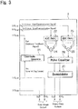
- a hybrid solid-state imaging device (two-dimensional image sensor) pertaining to an embodiment of the present invention encompasses a semiconductor chip 1 in which as illustrated in FIG. 1 , a pixel-array area 11 and a peripheral circuit portion (12, 13, 14, ---, 18 and 19) are integrated, and an external system 2 which communicates with the semiconductor chip 1 and mainly processes the optical-communication signal, and has a function that can carry out the image acquisition and the information acquisition through the optical communication, simultaneously.
- planar pattern in which the plurality of the pixels X i(2j-1) for the image signals and the plurality of the pixels X i(2j) for the optical-communication signals are arrayed alternately and periodically is merely used for the sake of an exemplification, the planar pattern is not limited to a topology illustrated in FIG. 2 .
- a periodical configuration may be used in which, after two pixel columns for the image signals are continuously arrayed, a pixel column for the optical-communication signal is mixed and arrayed on the third column.
- a periodical configuration may be used in which, after three pixel columns for the image signals are continuously arrayed, a pixel column for the optical-communication signal is arrayed on the fourth column.
- the pixels for the image signals and the pixels for the optical-communication signals may be mixed and arrayed alternately and periodically in the shape of a checkered pattern (check).
- Each of the pixels X i(2j-1) for the image signals and the pixels X i(2j) for the optical-communication signals may implement, for example, a rectangular imaging area.
- a comparator/latching circuit 14 for generating image signals, a correlative double sampling (CDS) circuit 15 and a horizontal read-out circuit 16 are provided along pixel rows X 11 to X 1m ; ------; X i1 to X im ; ------; X (n-2h)1 to X (n-2)m ; X (n-1)1 to X (n-1)m ; and X n1 to X nm directions.
- An X-address generator 17 for processing the optical-communication signals and a band-pass amplifier 18 are provided on the upper side of the pixel-array area 11.
- a row driver 12 for generating the image signals is provided along pixel columns X 11 , ------, X i1 ------, X (n-2)1 , X (n-1)1 , X n1 ; X 12 , ------, X i2 , ------; X (n-2)2 , X (n-1)2 , X n2 ; X 13, ------, X i3 , ------; X (n-2)3 , X (n-1)3 , X n3 ; ------; X 1(2j-1) , ------, X i(2j-1) , ------, X (n-2)(2j-1) , X (n-1)(2j-1) , X n(2j-1) ; ------; X 1(2j) , ------, X i(2j-1) , ------, X (n
- a Y-address generator 13 for processing the optical-communication signal is provided on the right side of the pixel-array area.
- a timing generator whose illustration is omitted is connected to the row driver 12 and the horizontal read-out circuit 16.
- the Y-address generator 13 and the X-address generator 17 are connected to each other through an address signal distributor 19.
- Each of the band-pass amplifier 18, the address signal distributor 19 and the comparator/latching circuit 14 is connected to the external system 2, and the external system 2 processes the optical-communication signal.
- the unit pixels X i(2j-1) , X i(2j) inside the pixel-array area 11 are sequentially scanned by the horizontal read-out circuit 16 and the row driver 12, and the reading out operation of the image signal and the processing of the image signal are executed.
- a gray image output is extracted through the external system 2 from the comparator/latching circuit 14 and the correlative double sampling circuit 15 via the vertical signal lines B 1 , B 3 , ---, B (2j-1) , --- on the odd-numbered columns, and the optical-communication signals are read out via the vertical signal lines B 2 B 4 , ---, B (2j) on the even-numbered columns.
- the hybrid solid-state imaging device pertaining to the embodiment of the present invention is established such that, since the pixel-array area 11 is vertically scanned at the units of the respective pixel rows X 11 to X 1m ; ------; X i1 to X im ; ------; X (n-2)1 to X (n-2)m ; X (n-1)1 to X (n-1)m ; and X n1 to X nm , with regard to the pixel signals of the respective pixel rows X 11 to X 1m ; ------, X i1 to X im ; ------; X (n-2)1 to X (n-2)m ; X (n-1)1 to X (n-1)m ; and X n1 to X mn , the pixel signals for the images are read out via the vertical signal lines B 1 , B 3 , ---, B (2j-1) , --- on the odd-numbered columns
- the pixel signals read out from the vertical signal lines B 1 , B 3 , ---, B (2j-1) , --- on the respective odd-numbered columns are signally processed in the correlative double sampling circuit 15, and then transferred as the gray image signals through the external system 2 via the amplifier in the correlative double sampling circuit 15.
- the optical-communication signals for each 3 ⁇ 3 block are read out to the band-pass amplifier 18 of 9 ⁇ 2 channels, and the optical-communication signals are processed by the external system 2.
- the external system 2 may be provided with, for example, an analog/digital converter (ADC), a field programmable gate array (FPGA) and the like.
- ADC analog/digital converter
- FPGA field programmable gate array
- the external system 2 includes a first AD converter 23 for feeding an optical-communication signal S CM1 of a first 3 ⁇ 3 block from the band-pass amplifier 18, through a first input/output node I/O 1 , a second AD converter 22 for feeding an optical-communication signals S CM2 of a second 3 ⁇ 3 block from the band-pass amplifier 18, through a second input/output node I/O 2 , a first adder 25 for synthesizing digital signals of nine channels that are A/D converted by the first AD converter 23, a second adder 24 for synthesizing digital signals of nine channels that are A/D converted by the second AD converter 22, a pulse equalizer 26 for equalizing an output pulse of the first adder 25 and an output pulse of the second adder 24, and a demodulator 27 for demodul
- FIG. 8 is the eye diagram to evaluate the quality of the pulses transferred from the pixel X i(2j) for the optical-communication signals on the even-numbered columns in the semiconductor chip 1 that are measured at 10 Mbps.
- the analog outputs S CM1 , S CM2 transferred from the band-pass amplifier 18 in the semiconductor chip 1 are digitized, with 10 bits 80MHz, by the AD converters 22, 23 in the external system 2. Then, in digital region, the digitized outputs are synthesized and monitored by the first adder 25 and the second adder 24.
- the raw overlapped waveform has a poor topology in which the eye height and the eye width of an opening (eye pattern) of the waveform trace are small, the characteristic of the waveform trace represents a deformed topology collapsing from the shape of a rectangular wave. As illustrated in FIG.
- the external system 2 further includes a coordinate generator 21 configured to determine an X-Y address for tracking the signal source of the optical signal, after acquiring a flag image signal S F1 of one bit through a fourth input/output node I/O 4 from the comparator/latching circuit 14, and then, the coordinate generator 21 transfers the X-Y address as an address feedback signal S AF through a third input/output node I/O 3 to the address signal distributor 19.
- a coordinate generator 21 configured to determine an X-Y address for tracking the signal source of the optical signal, after acquiring a flag image signal S F1 of one bit through a fourth input/output node I/O 4 from the comparator/latching circuit 14, and then, the coordinate generator 21 transfers the X-Y address as an address feedback signal S AF through a third input/output node I/O 3 to the address signal distributor 19.
- the address signal distributor 19 distributes the X-address determined by the coordinate generator 21 to the X-address generator 17 and distributes the Y-address to the Y-address generator 13 and determines the desirable 3 ⁇ 3 block from the pixels X 12 , ------, X i2 , ------, X (n-2)2 , X (n-1)2 , X n2 ; X 14 , ------, X i4 , ------, X (n-2)4 , X (n-1)4 , X n4 ; ------; X 1(2j) , ------, X i(2j) , ------, X (n-2)(2j) , X (n-1)(2j) , X n(2j) ; ------ on the respective even-numbered columns, and then tracks the signal source of the optical signals.
- the flag image signal S F1 of one bit supplied through the fourth input/output node I/O 4 from the comparator/latching circuit 14 and the respective image signals supplied through a fifth input/output node I/O 5 from the correlative double sampling circuit 15 are propagated as their original states of signals through the external system 2, and transferred as the gray images from the output node O 2 and the output node O 1 , respectively.
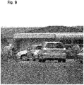
- FIG. 9 illustrates a gray image that is imaged by the pixels Xi (2j-1) for the image signals of the semiconductor chip 1 pertaining to the embodiment of the present invention
- FIG. 10 illustrates an image in which an image obtained by a camera of a QVGA resolution of 320 ⁇ 240 pixels is transmitted as optical signals from an LED light source side and then signally processed and reproduced by the pixels X i(2j) for the optical-communication signals in the semiconductor chip 1 pertaining to the embodiment of the present invention.
- FIG. 10(a) illustrates an image obtained by the CMOS camera having QVGA resolution.
- FIG. 10(b) illustrates a reproduced image of the image illustrated in FIG.
- the reproduced image is generated by the pixels X i(2j) for the optical-communication signals, after the optical signals of the image of FIG. 10(a) are transmitted at a carrier frequency of 5MHz by an infrared LED array of 10 ⁇ 10 (wavelength of 870mm).
- the coordinate generator 21 determines the X-Y address by using the flag image signals S F1 of one bit transferred from the comparator/latching circuit 14.
- the X-address generator 17 and the Y-address generator 13 drives the pixels X i(2j) for the predetermined optical-communication signals on the semiconductor chip 1, and the output signal from the pixels X i(2j) for the optical-communication signals is demodulated by using the demodulator 27 and reproduced as illustrated in FIG. 10(b) .
- a distance of an optical communication is 70m.
- the solid-state imaging device and the LED light source which pertain to the embodiment of the present invention, can be used to carry out the optical communication of a long distance of 50 meters or more and the solid-state imaging device pertaining to the embodiment of the present invention can be operated at a data signal speed enough to transmit the image signals.
- FIG. 11 illustrates a response characteristic of the hybrid solid-state imaging device, the response characteristic indicates a tracking performance to the LED light source, according to the hybrid solid-state imaging device pertaining to the embodiment of the present invention.
- FIG. 11 illustrates such that stable signals can be acquired within five micro seconds after the discovery of the candidate pixels.
- FIG. 11 exhibits an excellent performance of the hybrid solid-state imaging device in the application to the fields of vehicles, the performance is sufficient for the seamless real time tracking of the light source for the optical communication between road-to-vehicle or vehicle-to-vehicle.
- each of the pixels X 11 , ------, X i1 , ------, X (n-2)1 , X (n-1)1 , X n1 ; X 13 , ------, X 13 , ------; X (n-2)3 , X (n-1)3 , X n3 ; ------, X 1(2j-1) , ------, X i(2j-1) , ------, X (n-2)(2j-1) , X (n-1)(2j-1) , X n(2j-1) ; ------; X 1m , ------, X im , ------, X (n-2)m , X (n-1)m , and X nm adapted for the image signals, which are arranged on the odd-numbered columns in the pixels-array area 11 in the hybrid solid-state imaging device pertaining to the embodiment of the present invention may have the
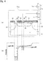
- FIG. 4(a) illustrates one example of the cross-sectional structure of the optical-information acquisition element that serves as the pixels X 12 , ------, X i2 , ------; X (n-2)2 , X (n-1)2 , X n2 , X 14 , ------, X i4 , ------, X (n-2)4 , X (n-1)4 , X n4 ; ------, X 1(2j) , ------, X i(2j) , ------, X (n-2)(2j) , X (n-1)(2j) , X n(2j) ; ------- adapted for the optical-communication signals, which are arranged on the even-numbered columns.
- the optical-information acquisition element X i(2j) pertaining to the embodiment of the present invention encompasses a semiconductor layer 31 of a first conductivity type (p-type). and a surface-buried region 33 of a second conductivity type (n-type) arranged on the semiconductor layer 31.
- the surface-buried region 33 serves as a light-receiving cathode region (charge-generation region), and the semiconductor layer 31 just under the surface-buried region (light-receiving cathode region) 33 serves as a light-receiving anode region. Consequently, the surface-buried region 33 and the semiconductor layer 31 implement the photodiode (33, 31).
- the circumference of the surface-buried region (light-receiving cathode region) 33 is surrounded by a well (p-well) 32 of the first conductivity type, arranged on the semiconductor layer 31.
- the p-well 32 is shown as if the p-wells 32 are divided into the right and left portions. However, the right and left portions are respectively merged at a near side portion and a deep rearward portion of the paper and exhibit an annular pattern in an actual planar pattern.
- the pinning layer 37 is the layer for suppressing the carriers from being generated on the surface at a dark time.
- the charge-exhaust region 34 is connected to the positive power supply potential (high-level power supply) V DD , and the charges (electrons) stored in the charge-exhaust region 34 are extracted toward the positive power supply potential (high-level power supply) V DD . That is, on the plan view (top view) whose illustration is omitted, the pinning layer 37, the charge-accumulation region 36, the barrier-creating region 35 and the charge-exhaust region 34 are arranged adjacently to each other, inside the pattern of the p-well 32 that is annularly arranged on the semiconductor layer 31. On the cross-sectional view of FIG.
- the pinning layer 37, the charge-accumulation region 36, the barrier-creating region 35 and the charge-exhaust region 34 are arranged in turn from the right side to the left side.
- the arrangement is not limited to the above.
- a topology in which the spinning layer 37, the charge-accumulation region 36, the barrier-creating region 35 and the charge-exhaust region 34 are arranged in turn from the left side to the right side may be used, and the array of the pinning layer 37, the charge-accumulation region 36, the barrier-creating region 35 and the charge-exhaust region 34 is not always located on a straight line.
- FIG. 4(a) exemplifies a case in which the semiconductor layer 31 of the first conductivity type (p-type) is used as "the semiconductor base-body region of the first conductivity type".
- the semiconductor layer 31 instead of the semiconductor layer 31, a double-level structure implemented by a semiconductor substrate of the first conductivity type (p + -type) whose impurity concentration is about 4 ⁇ 10 17 cm -3 or more and about 1 ⁇ 10 21 cm -3 or less, and an epitaxial growth layer of the first conductivity type (p-type) that is arranged on the semiconductor substrate having a lower impurity concentration than the semiconductor substrate is formed, and the epitaxial growth layer of the first conductivity type may be employed as "the semiconductor base-body region of the first conductivity type".
- a silicon epitaxial growth layer of the first conductivity type (p-type) is formed on the semiconductor substrate of the second conductivity type (n-type), and the epitaxial growth layer may be employed as the semiconductor layer 31 of the first conductivity type.
- the epitaxial growth layer of the first conductivity type (p-type) is formed on the semiconductor substrate of the second conductivity type (n-type) so as to form the pn junction, when the light having a longer wavelength penetrates into the deeper portion of the semiconductor substrate of the second conductivity type, because the potential barrier caused by the built-in potential of the pn junction disables the carriers, which are generated by the light in the semiconductor substrate of the second conductivity type, to penetrate into the epitaxial growth layer of the first conductivity type, the carriers generated in the deeper portion of the semiconductor substrate of the second conductivity type can be positively extracted.
- the pn junction can protect the carriers generated in the deeper position from being returned to upper portion through diffusion and leaked to the adjacent pixels. Therefore, the architecture of the pn junction structure achieves a technical advantage such that the pn junction disables the mixture of colors, in particular, in a case of an image sensor of a single-chip color in which color filters of RGB are provided.
- an insulation film 41 is formed so as to cover the surfaces of the pinning layer 37 and the barrier-creating region 35.
- contact windows are cut in the insulation film 41 so that surface wirings can be contacted to the charge-accumulation region 36 and the charge-exhaust region 34.
- the insulation film 41 although a silicon oxide film (SiO 2 ) is preferable, various insulation films other than the silicon oxide film (SiO 2 ) may be available.
- an ONO film implemented by a triple-level lamination film made of silicon oxide film (SiO 2 ) / silicon nitride film (Si 3 N 4 film) / silicon oxide film (SiO 2 ) may be available.
- the oxide that includes at least one element of strontium (Sr), aluminum (Al), magnesium (Mg), yttrium (Y), hafnium (Hf), zirconium (Zr), tantalum (Ta) and bismuth (Bi), or the silicon nitride that includes those elements, or the like can be used as the insulation film 41.
- a gate electrode of a read-out transistor Q A(2j) implementing an amplifier 15 whose equivalent circuit is indicated on the upper portion of the right side of FIG. 4(a) is connected, through a contact window being cut in the insulation film 41, to the charge-accumulation region 36.
- a drain electrode of the read-out transistor Q A(2j) is connected to the high-level power supply V DD , and a source electrode is connected to a drain electrode of a select transistor Q S(2j) .
- the semiconductor layer 31 is made of a silicon substrate whose impurity concentration is about 6 ⁇ 10 11 cm -3 or more and about 2 ⁇ 10 15 cm -3 or less, the standard CMOS process can be employed.
- the photodiode (33, 31), as illustrated in FIG. 4(a) is so formed that the n-type surface-buried region 33 is sandwiched, at both sides along the upper and lower directions, between the p-type semiconductor layer 31 and the p-type barrier-creating region 35, and consequently most of the surface-buried region 33 is depleted.
- the charge-accumulation region 36 is formed from the surface, and the potential level at the photodiode (33, 31) is applied through the charge-accumulation region 36 to the gate of the read-out transistor Q A(2j) for the source follower, and the potential level at the photodiode (33, 31) is read out through the vertical signal line B 2j to the outside.
- a potential barrier is created in a shape of a hill, the height of the hill is determined by the depleted potential level at the photodiode (33, 31).
- the potential barrier created between the charge-accumulation region 36 and the charge-exhaust region 34 can be designed by a similar design principle for creating a potential barrier in the channel of a junction type static induction transistor (SIT), which manifests the normally-off I-V characteristic.
- SIT junction type static induction transistor
- the n-type surface-buried region 33 is assumed to correspond to the channel region of the SIT
- the p-type semiconductor layer 31 and the p-type barrier-creating region 35 correspond to the gate regions of the SIT
- the n-type charge-accumulation region 36 corresponds to the source region of the SIT
- the n-type charge-exhaust region 34 corresponds to the drain region of the SIT
- FIG. 4(b) illustrates a potential profile of the conduction band on the surface of the semiconductor layer 31. That is, FIG. 4(b) is the potential diagram at a horizontal plane, in the cross-sectional view of FIG. 4(a) , by which the pinning layer 37 and the surface-buried region 33 just under the barrier-creating region 35 are cut at a horizontal level so as to include the bottoms of the charge-accumulation region 36 and the charge-exhaust region 34.
- charges (electrons) are indicated by closed circles.
- the case in which the first conductivity type is assigned as the p type, the second conductivity type is assigned as the n type, and the charges on which the process such as the transfer, the accumulation and the like is performed is assigned as electrons is exemplarily described.
- the lower direction (depth direction) of the drawing is represented as the positive direction of the potential, and the lower direction is the direction of the field to which the charges generated in the photodiode (33, 31) are transported.
- the electrical polarities become opposite, the charges to be processed become holes.
- the potential profile that indicates the potential barrier, potential valley, potential well and the like inside the optical-information acquisition element are represented such that the lower direction (depth direction) of the drawing is assigned as the negative direction of the potential.
- the lower direction of FIG. 4(b) is also the direction of the field to which charges (holes) generated in the photodiode are transported.
- a portion indicated by diagonal hatch pattern with upward oblique lines to the right is the potential level at which electrons are filled, and the top edge of the region indicated by the diagonal hatch pattern with the upward oblique lines to the right is the location of the Fermi level.
- the locations of the top edges of the regions indicated by the diagonal hatch pattern with the upward oblique lines to the right correspond to the locations (potential levels) of the bottom levels of the potential wells created by each of the charge-accumulation region 36 and the charge-exhaust region 34.
- the impurity concentrations of the surface-buried region 33, the barrier-creating region 35 and the charge-accumulation region 36 may be selected.
- the height of the potential barrier created between the charge-accumulation region 36 and the charge-exhaust region 34 can be determined on the basis of a perfectly depleted potential V d .
- V d a perfectly depleted potential created in the surface-buried region 33, which is caused by the p-type semiconductor layer 31 formed under the lower surface of the surface-buried region 33, is determined by the following Eq.
- x n indicates a width of the n-type region illustrated in FIG.
- x dp indicates a width of a depletion-layer of the p-type region when the n-type region is perfectly depleted
- N a indicates an acceptor concentration
- N d indicates a donor concentration.
- the value of the perfectly depleted potential V d is greater than the value of a built-in potential V bi of the pn junction in a thermal equilibrium state.
- the optical-information acquisition element pertaining to the embodiment of the present invention illustrated in FIG. 4(a) has a p-n-p structure in which differently from FIG. 5(a) , the n-type surface-buried region 33 is sandwiched, at both sides along the upper to lower directions, between the p-type semiconductor layer 31 and the p-type barrier-creating region 35.
- the height of the potential barrier can be determined by the design scheme similar to the design scheme of the height of potential barrier, which is determined by the height of the saddle point formed in the channel of the normally-off SIT.
- the height of the potential barrier created between the charge-accumulation region 36 and the charge-exhaust region 34 can be routinely determined on the basis of the respective impurity concentrations of the surface-buried region 33, the semiconductor layer 31, the barrier-creating region 35, the charge-accumulation region 36 and the charge-exhaust region 34, a distance between the semiconductor layer 31 and the barrier-creating region 35, a distance between the charge-accumulation region 36 and the charge-exhaust region 34, and a value of a voltage applied to the charge-exhaust region 34, which is similar to the design scheme of the normally-off SIT.
- I d I do exp ⁇ q ⁇ B / kT
- the optical current flowing into the charge-accumulation region 36 and the current flowing out from the charge-accumulation region 36 are balanced, the change in the potential level at the photodiode (33, 31) is stopped.
- the potential level of the charge-accumulation region 36 is assigned as V FD , the following Eq. (11) is established.
- the optical pulse When the optical pulse is turned off, the supply of the optical current is stopped, and because electrons flow out to the charge-exhaust region 34, the potential level at the photodiode (33, 31) increases as illustrated in FIG. 6(b) .
- the outflow current exhibits an exponential function of the height of the potential barrier, which is formed in the path to the charge-exhaust region 34. As the outflow of the charges to the charge-exhaust region 34 increases, the potential barrier becomes higher, and the outflow current is gradually decreased.
- the increase of the potential level at the photodiode (33, 31) continues until a next optical pulse is irradiated, as illustrated in FIG. 6(b) . As illustrated in FIG.
- the optical response illustrated in FIG. 6(b) can be understood. In this way, the potential level of the charge-accumulation region 36 responds to the on/off operations of the optical pulse and serves as an optical pulse receiving circuit.
- the equivalent capacitance of the optical-information acquisition element such as the parasitic capacitance C FD or the like is required to be made small.
- the potential profile of the photodiode (33, 31) portion is desirably shaped such that, as illustrated in FIG. 4(b) , an inclination of the potential level is created in the perfectly depleted potential V d so that electrons can be accelerated by an electric field toward the charge-accumulation region 36.
- the potential profile of the flow path toward the charge-exhaust region 34 from the charge-accumulation region 36 is desirably shaped such that the electric field is generated by the inclination of the potential level in the perfectly depleted potential V d .
- the architecture of providing the inclined potential profiles in the region where the potential inclination is created in the perfectly depleted potential V d , because the parasitic capacitance of the photodiode (33, 31) portion in the optical-information acquisition element cannot be generated, and only the capacitance associated with the limited region in which electrons are accumulated in the vicinity of the charge-accumulation region 36 shall be considered, the high-speed response of the optical-information acquisition element can be expected.
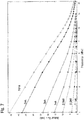
- FIG. 7 illustrates variations of the amplitudes of potentials at the charge-accumulation region 36 with respect to the variation of frequency of the pulse, as a measurement result.
- the intensity of the LED light source irradiating the optical-information acquisition element illustrated in FIG. 4 is changed, so that the intensity of the optical currents generated in the photodiode (33, 31) can be changed as 10nA, 5nA, 2nA, 1nA, 0.5nA, 0.2nA or 0.1nA.
- FIG. 7 illustrates such that, with respect to the pulse of the optical current of 10nA, the amplitude of about 9mV is obtained at 10MHz from the charge-accumulation region 36.
- the optical-information acquisition element pertaining to the embodiment of the present invention illustrated in FIG. 4(a) , it is possible to remove the reset transistors (36, 39) used in the earlier technology, which has been illustrated in FIG. 12 , and therefore, the reduction in the number of the elements and the simplification of the circuit configuration, and furthermore, reduction of the parasitic capacitance of the optical-information acquisition element are achieved, and therefore the optical-information acquisition element can carry out the high-speed response.
- the first conductivity type was assigned as the p type, and the second conductivity type was assigned as the n type.
- the first conductivity type could be assigned as the n type and the second conductivity type could be assigned as the p type.
- the similar effectiveness may be easily understood to be achieved when the electrical polarities are made opposite.
- the process such as the transfer operation, the accumulation operation and the like is performed is executed under the assumption that the charges to be processed are electrons, and in the potential diagram, the lower direction (depth direction) of the drawing is assigned as the positive direction of the potential.
- the potential profile that illustrates the potential barrier, the potential valley, the potential well and the like in the inside of the optical-information acquisition element shall be represented such that the lower direction (depth direction) of the drawing is the negative direction of the potential.
- the hybrid solid-state imaging device in which a plurality of the optical-information acquisition element and a plurality of the pixels for the image signals are merged and two-dimensionally arrayed is exemplarily described.
- the optical-information acquisition element in the present invention should not be construed limitedly to the application to only the pixels for the hybrid solid-state imaging device in the two-dimensional array.
- the hybrid solid-state imaging device in which a plurality of the optical-information acquisition element and a plurality of the pixels for the image signals are arrayed on the same semiconductor chip is exemplified.
- the realization of the configuration in which the pixels for the image signals is omitted and a plurality of the optical-information acquisition elements for the optical communication are two-dimensionally or one-dimensionally arrayed, configured to track the light source, can be easily understood from the subject matter of the above disclosure.
- FIG. 4(a) illustrates a configuration that the p-n-p structure in which the n-type surface-buried region 33 is sandwiched, at both sides along the upper to lower directions, between the p-type semiconductor layer 31 and the p-type barrier-creating region 35 is used to create the potential barrier between the charge-accumulation region 36 and the charge-exhaust region 34
- the configuration illustrated in FIG. 4(a) merely indicates an example.
- the p-type barrier-creating region 35 can be periodically buried in the shape of stripes in a certain depth of the n-type surface-buried region 33, and consequently, potential barriers can be created between the stripe-shaped barrier-creating regions 35 and the stripe-shaped barrier-creating regions 35.
- the p-type barrier-creating regions 35 may be formed in the bottoms or side walls of stripe-shaped grooves, which are periodically cut in the n-type surface-buried region 33, and the potential barrier may be created between the stripe-shaped barrier-creating region 35 and the stripe-shaped barrier-creating region 35. That is, similarly to the fact that there are various structures in normally-off SITs, there are various schemes by which the potential barriers are created between the charge-accumulation region 36 and the charge-exhaust region 34.
- the present invention can be used in the technical field such as the system or the like in which with the use of the spatial wireless communication through the light, the map information and the information adapted for safe driving of the vehicle can be transmitted and received between road-to-vehicle or between vehicle-to-vehicle.
Landscapes
- Engineering & Computer Science (AREA)
- Multimedia (AREA)
- Signal Processing (AREA)
- Solid State Image Pick-Up Elements (AREA)
- Transforming Light Signals Into Electric Signals (AREA)
Claims (3)
- Élément d'acquisition d'informations optiques comprenant :une couche semi-conductrice (31) d'un premier type de conductivité ;une région à surface enterrée (33) d'un second type de conductivité enterrée dans une partie d'une partie supérieure de la couche semi-conductrice (31) de manière à implémenter une photodiode avec la couche semi-conductrice ;une région d'accumulation de charges (36) du second type de conductivité enterrée dans une partie de la partie supérieure de la région à surface enterrée (33), configurée pour accumuler une partie de charges générées par la photodiode ;une région de création de barrière (35) du premier type de conductivité enterrée à proximité adjacente de la région d'accumulation de charges (36) dans une partie de la partie supérieure de la région à surface enterrée (33), dans lequel des concentrations en impuretés de la région à surface enterrée (33), de la région de création de barrière (35) et de la couche semi-conductrice (31) sont respectivement sélectionnées de sorte qu'une partie de la région à surface enterrée (33) entre la région de création de barrière (35) et la couche semi-conductrice (31) est parfaitement appauvrie, de manière à créer une barrière de potentiel dans la partie parfaitement appauvrie de la région à surface enterrée (33) à l'encontre d'un déversement des charges accumulées dans la région d'accumulation de charges ; etune région d'évacuation de charges (34) du second type de conductivité enterrée à proximité adjacente de la région à surface enterrée (33) dans une zone limitée de la partie supérieure de la couche semi-conductrice (31), qui est en contact avec la région à surface enterrée (33) de manière à définir un trajet de charges en excès depuis la région d'accumulation de charges (36) via la barrière de potentiel en direction de la région d'évacuation de charges (34), et qui est configurée pour stocker et extraire les charges en excès qui franchissent la barrière de potentiel et se déversent depuis la région d'accumulation de charges (36) à travers le trajet ; etun câblage connecté à la région d'accumulation de charges (36), dans lequel le câblage est configuré pour extraire des changements de niveau de potentiel de la région d'accumulation de charges, déterminés par les charges accumulées dans la région d'accumulation de charges sur la base d'une hauteur de la barrière de potentiel en association avec des opérations marche et arrêt de signaux de communication optiques, en tant que signaux.
- Réseau d'éléments d'acquisition d'informations optiques comprenant une pluralité d'éléments d'acquisition d'informations optiques selon la revendication 1, la pluralité d'éléments d'acquisition d'informations optiques étant disposée en réseau sur une même puce semi-conductrice (1),
dans lequel des changements de niveau de potentiel de la région d'accumulation de charges (36) sont extraits en tant que signaux depuis chacun de la pluralité d'éléments d'acquisition d'informations optiques. - Dispositif d'imagerie à solide hybride comprenant une pluralité d'éléments d'acquisition d'informations optiques selon la revendication 1, la pluralité d'éléments d'acquisition d'informations optiques étant disposée en réseau sur une puce semi-conductrice (1) ; et
une pluralité de pixels (Xi) pour détecter des signaux d'image, disposés en réseau sur la même puce semi-conductrice (1), qui sont fusionnés à la pluralité des éléments d'acquisition d'informations optiques,
dans lequel des changements de niveau de potentiel de la région d'accumulation de charges (36) sont extraits en tant que signaux depuis chacun de la pluralité d'éléments d'acquisition d'informations optiques, et les signaux d'image sont extraits respectivement à partir de la pluralité de pixels (Xi) pour les signaux d'image.
Applications Claiming Priority (2)
| Application Number | Priority Date | Filing Date | Title |
|---|---|---|---|
| JP2010024791 | 2010-02-05 | ||
| PCT/JP2011/052447 WO2011096549A1 (fr) | 2010-02-05 | 2011-02-04 | Élément d'acquisition d'informations optiques, réseau d'éléments d'acquisition d'informations optiques, et dispositif de prise de vue à semi-conducteur hybride |
Publications (3)
| Publication Number | Publication Date |
|---|---|
| EP2533287A1 EP2533287A1 (fr) | 2012-12-12 |
| EP2533287A4 EP2533287A4 (fr) | 2014-04-02 |
| EP2533287B1 true EP2533287B1 (fr) | 2018-04-18 |
Family
ID=44355543
Family Applications (1)
| Application Number | Title | Priority Date | Filing Date |
|---|---|---|---|
| EP11739897.4A Not-in-force EP2533287B1 (fr) | 2010-02-05 | 2011-02-04 | Élément d'acquisition d'informations optiques, réseau d'éléments d'acquisition d'informations optiques, et dispositif de prise de vue à semi-conducteur hybride |
Country Status (5)
| Country | Link |
|---|---|
| US (1) | US8907388B2 (fr) |
| EP (1) | EP2533287B1 (fr) |
| JP (1) | JP5648964B2 (fr) |
| KR (1) | KR101312083B1 (fr) |
| WO (1) | WO2011096549A1 (fr) |
Families Citing this family (7)
| Publication number | Priority date | Publication date | Assignee | Title |
|---|---|---|---|---|
| JP5648922B2 (ja) * | 2009-10-05 | 2015-01-07 | 国立大学法人静岡大学 | 半導体素子及び固体撮像装置 |
| KR20150133968A (ko) * | 2014-05-21 | 2015-12-01 | 삼성전자주식회사 | 비동기 통신회로, 및 이를 포함하는 세탁기 |
| US9812604B2 (en) * | 2014-05-30 | 2017-11-07 | Klaus Y. J. Hsu | Photosensing device with graphene |
| US9812603B2 (en) * | 2014-05-30 | 2017-11-07 | Klaus Y. J. Hsu | Photosensing device with graphene |
| JP6351097B2 (ja) * | 2014-06-20 | 2018-07-04 | 国立大学法人静岡大学 | 電磁波検出素子及び固体撮像装置 |
| WO2018038230A1 (fr) * | 2016-08-24 | 2018-03-01 | 国立大学法人静岡大学 | Élément de conversion photoélectrique et dispositif de capture d'image à semi-conducteur |
| US10854129B2 (en) | 2018-06-18 | 2020-12-01 | Apple Inc. | Hybrid architecture for zero border display |
Family Cites Families (18)
| Publication number | Priority date | Publication date | Assignee | Title |
|---|---|---|---|---|
| JPS62230273A (ja) | 1986-03-31 | 1987-10-08 | Toshiba Corp | 固体撮像装置 |
| JPH0766981B2 (ja) * | 1987-03-26 | 1995-07-19 | 日本電気株式会社 | 赤外線センサ |
| JPH05251684A (ja) | 1991-11-25 | 1993-09-28 | Eastman Kodak Co | ブルーミング防止特性を向上させたccd画像センサ |
| JPH0689998A (ja) | 1992-09-07 | 1994-03-29 | Sony Corp | 固体撮像装置 |
| JPH06338524A (ja) * | 1993-03-31 | 1994-12-06 | Toshiba Corp | 電荷転送装置 |
| US5903021A (en) | 1997-01-17 | 1999-05-11 | Eastman Kodak Company | Partially pinned photodiode for solid state image sensors |
| JP3413078B2 (ja) * | 1997-10-06 | 2003-06-03 | キヤノン株式会社 | 光電変換装置と密着型イメージセンサ |
| US6372537B1 (en) * | 2000-03-17 | 2002-04-16 | Taiwan Semiconductor Manufacturing Company | Pinned photodiode structure in a 3T active pixel sensor |
| FR2820882B1 (fr) | 2001-02-12 | 2003-06-13 | St Microelectronics Sa | Photodetecteur a trois transistors |
| JP4288346B2 (ja) * | 2003-08-19 | 2009-07-01 | 国立大学法人静岡大学 | 撮像装置及び画素回路 |
| WO2007026779A1 (fr) * | 2005-08-30 | 2007-03-08 | National University Corporation Shizuoka University | Élément de mesure de distance semi-conducteur et dispositif d’imagerie à l’état solide |
| JP5110519B2 (ja) * | 2005-08-30 | 2012-12-26 | 国立大学法人静岡大学 | 半導体測距素子及び固体撮像装置 |
| JP5110535B2 (ja) * | 2006-03-31 | 2012-12-26 | 国立大学法人静岡大学 | 半導体測距素子及び固体撮像装置 |
| WO2008069141A1 (fr) * | 2006-11-30 | 2008-06-12 | National University Corporation Shizuoka University | Élément semi-conducteur de mesure de distance et dispositif semi-conducteur d'imagerie |
| JP5283216B2 (ja) * | 2008-07-31 | 2013-09-04 | 国立大学法人静岡大学 | 高速電荷転送フォトダイオード、ロックインピクセル及び固体撮像装置 |
| JP5688756B2 (ja) | 2008-12-25 | 2015-03-25 | 国立大学法人静岡大学 | 半導体素子及び固体撮像装置 |
| JP5271104B2 (ja) | 2009-02-13 | 2013-08-21 | 浜松ホトニクス株式会社 | リニアイメージセンサ |
| EP2487714B1 (fr) * | 2009-10-09 | 2018-12-05 | National University Corporation Shizuoka University | Élément semi-conducteur et dispositif à l'état solide de capture d'images |
-
2011
- 2011-02-04 WO PCT/JP2011/052447 patent/WO2011096549A1/fr not_active Ceased
- 2011-02-04 US US13/577,112 patent/US8907388B2/en not_active Expired - Fee Related
- 2011-02-04 JP JP2011552848A patent/JP5648964B2/ja not_active Expired - Fee Related
- 2011-02-04 EP EP11739897.4A patent/EP2533287B1/fr not_active Not-in-force
- 2011-02-04 KR KR1020127021443A patent/KR101312083B1/ko not_active Expired - Fee Related
Non-Patent Citations (1)
| Title |
|---|
| None * |
Also Published As
| Publication number | Publication date |
|---|---|
| JPWO2011096549A1 (ja) | 2013-06-13 |
| US20120301150A1 (en) | 2012-11-29 |
| JP5648964B2 (ja) | 2015-01-07 |
| KR20120114359A (ko) | 2012-10-16 |
| EP2533287A1 (fr) | 2012-12-12 |
| KR101312083B1 (ko) | 2013-09-26 |
| EP2533287A4 (fr) | 2014-04-02 |
| US8907388B2 (en) | 2014-12-09 |
| WO2011096549A1 (fr) | 2011-08-11 |
Similar Documents
| Publication | Publication Date | Title |
|---|---|---|
| EP2533287B1 (fr) | Élément d'acquisition d'informations optiques, réseau d'éléments d'acquisition d'informations optiques, et dispositif de prise de vue à semi-conducteur hybride | |
| EP2974279B1 (fr) | Photodétecteur ayant une sensibilité améliorée | |
| CN108257991B (zh) | 固态成像器件、成像系统和可移动物体 | |
| KR101508410B1 (ko) | 거리 화상 센서, 및 촬상 신호를 비행시간법에 의해 생성하는 방법 | |
| US10636822B2 (en) | Photoelectric conversion element and solid-state image capturing device | |
| US20170221220A1 (en) | Distance sensor and image processing system including the same | |
| US8891978B2 (en) | Information-acquisition device and optical communication system | |
| EP3497470B1 (fr) | Démodulateur avec une photodiode de type pinned générant des porteurs de charge et son procédé d'utilisation | |
| CN108632544A (zh) | 固态成像设备、成像系统和能移动的物体 | |
| US9307171B2 (en) | Solid state image pick-up device, and pixel | |
| JP2010056345A (ja) | 増幅型固体撮像装置 | |
| KR20170096601A (ko) | Hdr 픽셀 | |
| US20040201047A1 (en) | Solid-state imaging device | |
| EP3352220A1 (fr) | Élément semiconducteur et dispositif d'imagerie à semiconducteur | |
| JP2023061391A (ja) | イメージセンシング装置 | |
| US12068342B2 (en) | Photoelectric conversion device, imaging system, and movable body | |
| CN114697580B (zh) | 图像感测装置 | |
| KR102883963B1 (ko) | 이미지 센싱 장치 | |
| JP4647801B2 (ja) | 半導体エネルギー線検出器 | |
| KR20220072257A (ko) | 이미지 센싱 장치 | |
| KR20210151497A (ko) | 이미지 센싱 장치 | |
| US20220278163A1 (en) | Image sensing device | |
| KR20230116402A (ko) | 이미지 센싱 장치 | |
| JP2012216693A (ja) | 受光装置 | |
| JP2006094136A (ja) | 固体撮像装置 |
Legal Events
| Date | Code | Title | Description |
|---|---|---|---|
| PUAI | Public reference made under article 153(3) epc to a published international application that has entered the european phase |
Free format text: ORIGINAL CODE: 0009012 |
|
| 17P | Request for examination filed |
Effective date: 20120830 |
|
| AK | Designated contracting states |
Kind code of ref document: A1 Designated state(s): AL AT BE BG CH CY CZ DE DK EE ES FI FR GB GR HR HU IE IS IT LI LT LU LV MC MK MT NL NO PL PT RO RS SE SI SK SM TR |
|
| DAX | Request for extension of the european patent (deleted) | ||
| A4 | Supplementary search report drawn up and despatched |
Effective date: 20140305 |
|
| RIC1 | Information provided on ipc code assigned before grant |
Ipc: H01L 27/146 20060101ALI20140227BHEP Ipc: H01L 27/14 20060101AFI20140227BHEP Ipc: H04N 5/3745 20110101ALI20140227BHEP |
|
| REG | Reference to a national code |
Ref country code: DE Ref legal event code: R079 Ref document number: 602011047583 Country of ref document: DE Free format text: PREVIOUS MAIN CLASS: H01L0027140000 Ipc: H01L0027146000 |
|
| RIC1 | Information provided on ipc code assigned before grant |
Ipc: H04N 5/3745 20110101ALI20170915BHEP Ipc: H01L 27/146 20060101AFI20170915BHEP |
|
| GRAP | Despatch of communication of intention to grant a patent |
Free format text: ORIGINAL CODE: EPIDOSNIGR1 |
|
| STAA | Information on the status of an ep patent application or granted ep patent |
Free format text: STATUS: GRANT OF PATENT IS INTENDED |
|
| INTG | Intention to grant announced |
Effective date: 20171030 |
|
| GRAS | Grant fee paid |
Free format text: ORIGINAL CODE: EPIDOSNIGR3 |
|
| GRAA | (expected) grant |
Free format text: ORIGINAL CODE: 0009210 |
|
| STAA | Information on the status of an ep patent application or granted ep patent |
Free format text: STATUS: THE PATENT HAS BEEN GRANTED |
|
| AK | Designated contracting states |
Kind code of ref document: B1 Designated state(s): AL AT BE BG CH CY CZ DE DK EE ES FI FR GB GR HR HU IE IS IT LI LT LU LV MC MK MT NL NO PL PT RO RS SE SI SK SM TR |
|
| REG | Reference to a national code |
Ref country code: GB Ref legal event code: FG4D |
|
| REG | Reference to a national code |
Ref country code: CH Ref legal event code: EP |
|
| REG | Reference to a national code |
Ref country code: AT Ref legal event code: REF Ref document number: 991327 Country of ref document: AT Kind code of ref document: T Effective date: 20180515 |
|
| REG | Reference to a national code |
Ref country code: IE Ref legal event code: FG4D |
|
| REG | Reference to a national code |
Ref country code: DE Ref legal event code: R096 Ref document number: 602011047583 Country of ref document: DE |
|
| REG | Reference to a national code |
Ref country code: NL Ref legal event code: MP Effective date: 20180418 |
|
| REG | Reference to a national code |
Ref country code: LT Ref legal event code: MG4D |
|
| PG25 | Lapsed in a contracting state [announced via postgrant information from national office to epo] |
Ref country code: NL Free format text: LAPSE BECAUSE OF FAILURE TO SUBMIT A TRANSLATION OF THE DESCRIPTION OR TO PAY THE FEE WITHIN THE PRESCRIBED TIME-LIMIT Effective date: 20180418 |
|
| PG25 | Lapsed in a contracting state [announced via postgrant information from national office to epo] |
Ref country code: AL Free format text: LAPSE BECAUSE OF FAILURE TO SUBMIT A TRANSLATION OF THE DESCRIPTION OR TO PAY THE FEE WITHIN THE PRESCRIBED TIME-LIMIT Effective date: 20180418 Ref country code: PL Free format text: LAPSE BECAUSE OF FAILURE TO SUBMIT A TRANSLATION OF THE DESCRIPTION OR TO PAY THE FEE WITHIN THE PRESCRIBED TIME-LIMIT Effective date: 20180418 Ref country code: LT Free format text: LAPSE BECAUSE OF FAILURE TO SUBMIT A TRANSLATION OF THE DESCRIPTION OR TO PAY THE FEE WITHIN THE PRESCRIBED TIME-LIMIT Effective date: 20180418 Ref country code: ES Free format text: LAPSE BECAUSE OF FAILURE TO SUBMIT A TRANSLATION OF THE DESCRIPTION OR TO PAY THE FEE WITHIN THE PRESCRIBED TIME-LIMIT Effective date: 20180418 Ref country code: NO Free format text: LAPSE BECAUSE OF FAILURE TO SUBMIT A TRANSLATION OF THE DESCRIPTION OR TO PAY THE FEE WITHIN THE PRESCRIBED TIME-LIMIT Effective date: 20180718 Ref country code: SE Free format text: LAPSE BECAUSE OF FAILURE TO SUBMIT A TRANSLATION OF THE DESCRIPTION OR TO PAY THE FEE WITHIN THE PRESCRIBED TIME-LIMIT Effective date: 20180418 Ref country code: FI Free format text: LAPSE BECAUSE OF FAILURE TO SUBMIT A TRANSLATION OF THE DESCRIPTION OR TO PAY THE FEE WITHIN THE PRESCRIBED TIME-LIMIT Effective date: 20180418 Ref country code: BG Free format text: LAPSE BECAUSE OF FAILURE TO SUBMIT A TRANSLATION OF THE DESCRIPTION OR TO PAY THE FEE WITHIN THE PRESCRIBED TIME-LIMIT Effective date: 20180718 |
|
| PG25 | Lapsed in a contracting state [announced via postgrant information from national office to epo] |
Ref country code: GR Free format text: LAPSE BECAUSE OF FAILURE TO SUBMIT A TRANSLATION OF THE DESCRIPTION OR TO PAY THE FEE WITHIN THE PRESCRIBED TIME-LIMIT Effective date: 20180719 Ref country code: RS Free format text: LAPSE BECAUSE OF FAILURE TO SUBMIT A TRANSLATION OF THE DESCRIPTION OR TO PAY THE FEE WITHIN THE PRESCRIBED TIME-LIMIT Effective date: 20180418 Ref country code: LV Free format text: LAPSE BECAUSE OF FAILURE TO SUBMIT A TRANSLATION OF THE DESCRIPTION OR TO PAY THE FEE WITHIN THE PRESCRIBED TIME-LIMIT Effective date: 20180418 Ref country code: HR Free format text: LAPSE BECAUSE OF FAILURE TO SUBMIT A TRANSLATION OF THE DESCRIPTION OR TO PAY THE FEE WITHIN THE PRESCRIBED TIME-LIMIT Effective date: 20180418 |
|
| REG | Reference to a national code |
Ref country code: AT Ref legal event code: MK05 Ref document number: 991327 Country of ref document: AT Kind code of ref document: T Effective date: 20180418 |
|
| PG25 | Lapsed in a contracting state [announced via postgrant information from national office to epo] |
Ref country code: PT Free format text: LAPSE BECAUSE OF FAILURE TO SUBMIT A TRANSLATION OF THE DESCRIPTION OR TO PAY THE FEE WITHIN THE PRESCRIBED TIME-LIMIT Effective date: 20180820 |
|
| REG | Reference to a national code |
Ref country code: DE Ref legal event code: R097 Ref document number: 602011047583 Country of ref document: DE |
|
| PG25 | Lapsed in a contracting state [announced via postgrant information from national office to epo] |
Ref country code: SK Free format text: LAPSE BECAUSE OF FAILURE TO SUBMIT A TRANSLATION OF THE DESCRIPTION OR TO PAY THE FEE WITHIN THE PRESCRIBED TIME-LIMIT Effective date: 20180418 Ref country code: AT Free format text: LAPSE BECAUSE OF FAILURE TO SUBMIT A TRANSLATION OF THE DESCRIPTION OR TO PAY THE FEE WITHIN THE PRESCRIBED TIME-LIMIT Effective date: 20180418 Ref country code: DK Free format text: LAPSE BECAUSE OF FAILURE TO SUBMIT A TRANSLATION OF THE DESCRIPTION OR TO PAY THE FEE WITHIN THE PRESCRIBED TIME-LIMIT Effective date: 20180418 Ref country code: EE Free format text: LAPSE BECAUSE OF FAILURE TO SUBMIT A TRANSLATION OF THE DESCRIPTION OR TO PAY THE FEE WITHIN THE PRESCRIBED TIME-LIMIT Effective date: 20180418 Ref country code: CZ Free format text: LAPSE BECAUSE OF FAILURE TO SUBMIT A TRANSLATION OF THE DESCRIPTION OR TO PAY THE FEE WITHIN THE PRESCRIBED TIME-LIMIT Effective date: 20180418 Ref country code: RO Free format text: LAPSE BECAUSE OF FAILURE TO SUBMIT A TRANSLATION OF THE DESCRIPTION OR TO PAY THE FEE WITHIN THE PRESCRIBED TIME-LIMIT Effective date: 20180418 |
|
| PLBE | No opposition filed within time limit |
Free format text: ORIGINAL CODE: 0009261 |
|
| STAA | Information on the status of an ep patent application or granted ep patent |
Free format text: STATUS: NO OPPOSITION FILED WITHIN TIME LIMIT |
|
| PG25 | Lapsed in a contracting state [announced via postgrant information from national office to epo] |
Ref country code: IT Free format text: LAPSE BECAUSE OF FAILURE TO SUBMIT A TRANSLATION OF THE DESCRIPTION OR TO PAY THE FEE WITHIN THE PRESCRIBED TIME-LIMIT Effective date: 20180418 Ref country code: SM Free format text: LAPSE BECAUSE OF FAILURE TO SUBMIT A TRANSLATION OF THE DESCRIPTION OR TO PAY THE FEE WITHIN THE PRESCRIBED TIME-LIMIT Effective date: 20180418 |
|
| 26N | No opposition filed |
Effective date: 20190121 |
|
| PG25 | Lapsed in a contracting state [announced via postgrant information from national office to epo] |
Ref country code: SI Free format text: LAPSE BECAUSE OF FAILURE TO SUBMIT A TRANSLATION OF THE DESCRIPTION OR TO PAY THE FEE WITHIN THE PRESCRIBED TIME-LIMIT Effective date: 20180418 |
|
| REG | Reference to a national code |
Ref country code: DE Ref legal event code: R119 Ref document number: 602011047583 Country of ref document: DE |
|
| REG | Reference to a national code |
Ref country code: CH Ref legal event code: PL |
|
| GBPC | Gb: european patent ceased through non-payment of renewal fee |
Effective date: 20190204 |
|
| PG25 | Lapsed in a contracting state [announced via postgrant information from national office to epo] |
Ref country code: LU Free format text: LAPSE BECAUSE OF NON-PAYMENT OF DUE FEES Effective date: 20190204 Ref country code: MC Free format text: LAPSE BECAUSE OF FAILURE TO SUBMIT A TRANSLATION OF THE DESCRIPTION OR TO PAY THE FEE WITHIN THE PRESCRIBED TIME-LIMIT Effective date: 20180418 |
|
| REG | Reference to a national code |
Ref country code: BE Ref legal event code: MM Effective date: 20190228 |
|
| REG | Reference to a national code |
Ref country code: IE Ref legal event code: MM4A |
|
| PG25 | Lapsed in a contracting state [announced via postgrant information from national office to epo] |
Ref country code: CH Free format text: LAPSE BECAUSE OF NON-PAYMENT OF DUE FEES Effective date: 20190228 Ref country code: LI Free format text: LAPSE BECAUSE OF NON-PAYMENT OF DUE FEES Effective date: 20190228 |
|
| PG25 | Lapsed in a contracting state [announced via postgrant information from national office to epo] |
Ref country code: GB Free format text: LAPSE BECAUSE OF NON-PAYMENT OF DUE FEES Effective date: 20190204 Ref country code: IE Free format text: LAPSE BECAUSE OF NON-PAYMENT OF DUE FEES Effective date: 20190204 Ref country code: DE Free format text: LAPSE BECAUSE OF NON-PAYMENT OF DUE FEES Effective date: 20190903 |
|
| PG25 | Lapsed in a contracting state [announced via postgrant information from national office to epo] |
Ref country code: FR Free format text: LAPSE BECAUSE OF NON-PAYMENT OF DUE FEES Effective date: 20190228 Ref country code: BE Free format text: LAPSE BECAUSE OF NON-PAYMENT OF DUE FEES Effective date: 20190228 |
|
| PG25 | Lapsed in a contracting state [announced via postgrant information from national office to epo] |
Ref country code: TR Free format text: LAPSE BECAUSE OF FAILURE TO SUBMIT A TRANSLATION OF THE DESCRIPTION OR TO PAY THE FEE WITHIN THE PRESCRIBED TIME-LIMIT Effective date: 20180418 |
|
| PG25 | Lapsed in a contracting state [announced via postgrant information from national office to epo] |
Ref country code: MT Free format text: LAPSE BECAUSE OF NON-PAYMENT OF DUE FEES Effective date: 20190204 |
|
| PG25 | Lapsed in a contracting state [announced via postgrant information from national office to epo] |
Ref country code: CY Free format text: LAPSE BECAUSE OF FAILURE TO SUBMIT A TRANSLATION OF THE DESCRIPTION OR TO PAY THE FEE WITHIN THE PRESCRIBED TIME-LIMIT Effective date: 20180418 |
|
| PG25 | Lapsed in a contracting state [announced via postgrant information from national office to epo] |
Ref country code: IS Free format text: LAPSE BECAUSE OF FAILURE TO SUBMIT A TRANSLATION OF THE DESCRIPTION OR TO PAY THE FEE WITHIN THE PRESCRIBED TIME-LIMIT Effective date: 20180818 |
|
| PG25 | Lapsed in a contracting state [announced via postgrant information from national office to epo] |
Ref country code: HU Free format text: LAPSE BECAUSE OF FAILURE TO SUBMIT A TRANSLATION OF THE DESCRIPTION OR TO PAY THE FEE WITHIN THE PRESCRIBED TIME-LIMIT; INVALID AB INITIO Effective date: 20110204 |
|
| PG25 | Lapsed in a contracting state [announced via postgrant information from national office to epo] |
Ref country code: MK Free format text: LAPSE BECAUSE OF FAILURE TO SUBMIT A TRANSLATION OF THE DESCRIPTION OR TO PAY THE FEE WITHIN THE PRESCRIBED TIME-LIMIT Effective date: 20180418 |