EP2540780B1 - Zusammensetzung zur Bildung einer Resistunterschichtfolie, und Strukturierungsverfahren - Google Patents
Zusammensetzung zur Bildung einer Resistunterschichtfolie, und Strukturierungsverfahren Download PDFInfo
- Publication number
- EP2540780B1 EP2540780B1 EP12004626.3A EP12004626A EP2540780B1 EP 2540780 B1 EP2540780 B1 EP 2540780B1 EP 12004626 A EP12004626 A EP 12004626A EP 2540780 B1 EP2540780 B1 EP 2540780B1
- Authority
- EP
- European Patent Office
- Prior art keywords
- silicon
- underlayer film
- film
- pattern
- resist underlayer
- Prior art date
- Legal status (The legal status is an assumption and is not a legal conclusion. Google has not performed a legal analysis and makes no representation as to the accuracy of the status listed.)
- Active
Links
- 0 CCO*(C1)=CC(OC2(C)CCCCC2)=C[*@](C)C=C[C@@]1(C)C=CC Chemical compound CCO*(C1)=CC(OC2(C)CCCCC2)=C[*@](C)C=C[C@@]1(C)C=CC 0.000 description 5
- XDTMQSROBMDMFD-UHFFFAOYSA-N C1CCCCC1 Chemical compound C1CCCCC1 XDTMQSROBMDMFD-UHFFFAOYSA-N 0.000 description 1
- UOBWBMQJMISIRD-UHFFFAOYSA-N CCC(C)(C)C(OC(C1OC2C3C1)C2OC3=O)=O Chemical compound CCC(C)(C)C(OC(C1OC2C3C1)C2OC3=O)=O UOBWBMQJMISIRD-UHFFFAOYSA-N 0.000 description 1
- LDMSFMSZAIXXBC-UHFFFAOYSA-N CCC(C)(C)C(OC(CC(C1)C2)(CC1(C1)OC(C(C)C)OC)CC21OC(C(C)C)OC)=O Chemical compound CCC(C)(C)C(OC(CC(C1)C2)(CC1(C1)OC(C(C)C)OC)CC21OC(C(C)C)OC)=O LDMSFMSZAIXXBC-UHFFFAOYSA-N 0.000 description 1
Images
Classifications
-
- C—CHEMISTRY; METALLURGY
- C09—DYES; PAINTS; POLISHES; NATURAL RESINS; ADHESIVES; COMPOSITIONS NOT OTHERWISE PROVIDED FOR; APPLICATIONS OF MATERIALS NOT OTHERWISE PROVIDED FOR
- C09D—COATING COMPOSITIONS, e.g. PAINTS, VARNISHES OR LACQUERS; FILLING PASTES; CHEMICAL PAINT OR INK REMOVERS; INKS; CORRECTING FLUIDS; WOODSTAINS; PASTES OR SOLIDS FOR COLOURING OR PRINTING; USE OF MATERIALS THEREFOR
- C09D183/00—Coating compositions based on macromolecular compounds obtained by reactions forming in the main chain of the macromolecule a linkage containing silicon, with or without sulfur, nitrogen, oxygen, or carbon only; Coating compositions based on derivatives of such polymers
- C09D183/04—Polysiloxanes
- C09D183/06—Polysiloxanes containing silicon bound to oxygen-containing groups
-
- C—CHEMISTRY; METALLURGY
- C08—ORGANIC MACROMOLECULAR COMPOUNDS; THEIR PREPARATION OR CHEMICAL WORKING-UP; COMPOSITIONS BASED THEREON
- C08L—COMPOSITIONS OF MACROMOLECULAR COMPOUNDS
- C08L83/00—Compositions of macromolecular compounds obtained by reactions forming in the main chain of the macromolecule a linkage containing silicon with or without sulfur, nitrogen, oxygen or carbon only; Compositions of derivatives of such polymers
- C08L83/04—Polysiloxanes
- C08L83/06—Polysiloxanes containing silicon bound to oxygen-containing groups
-
- G—PHYSICS
- G03—PHOTOGRAPHY; CINEMATOGRAPHY; ANALOGOUS TECHNIQUES USING WAVES OTHER THAN OPTICAL WAVES; ELECTROGRAPHY; HOLOGRAPHY
- G03F—PHOTOMECHANICAL PRODUCTION OF TEXTURED OR PATTERNED SURFACES, e.g. FOR PRINTING, FOR PROCESSING OF SEMICONDUCTOR DEVICES; MATERIALS THEREFOR; ORIGINALS THEREFOR; APPARATUS SPECIALLY ADAPTED THEREFOR
- G03F7/00—Photomechanical, e.g. photolithographic, production of textured or patterned surfaces, e.g. printing surfaces; Materials therefor, e.g. comprising photoresists; Apparatus specially adapted therefor
- G03F7/004—Photosensitive materials
- G03F7/075—Silicon-containing compounds
- G03F7/0751—Silicon-containing compounds used as adhesion-promoting additives or as means to improve adhesion
-
- G—PHYSICS
- G03—PHOTOGRAPHY; CINEMATOGRAPHY; ANALOGOUS TECHNIQUES USING WAVES OTHER THAN OPTICAL WAVES; ELECTROGRAPHY; HOLOGRAPHY
- G03F—PHOTOMECHANICAL PRODUCTION OF TEXTURED OR PATTERNED SURFACES, e.g. FOR PRINTING, FOR PROCESSING OF SEMICONDUCTOR DEVICES; MATERIALS THEREFOR; ORIGINALS THEREFOR; APPARATUS SPECIALLY ADAPTED THEREFOR
- G03F7/00—Photomechanical, e.g. photolithographic, production of textured or patterned surfaces, e.g. printing surfaces; Materials therefor, e.g. comprising photoresists; Apparatus specially adapted therefor
- G03F7/004—Photosensitive materials
- G03F7/075—Silicon-containing compounds
- G03F7/0752—Silicon-containing compounds in non photosensitive layers or as additives, e.g. for dry lithography
-
- G—PHYSICS
- G03—PHOTOGRAPHY; CINEMATOGRAPHY; ANALOGOUS TECHNIQUES USING WAVES OTHER THAN OPTICAL WAVES; ELECTROGRAPHY; HOLOGRAPHY
- G03F—PHOTOMECHANICAL PRODUCTION OF TEXTURED OR PATTERNED SURFACES, e.g. FOR PRINTING, FOR PROCESSING OF SEMICONDUCTOR DEVICES; MATERIALS THEREFOR; ORIGINALS THEREFOR; APPARATUS SPECIALLY ADAPTED THEREFOR
- G03F7/00—Photomechanical, e.g. photolithographic, production of textured or patterned surfaces, e.g. printing surfaces; Materials therefor, e.g. comprising photoresists; Apparatus specially adapted therefor
- G03F7/004—Photosensitive materials
- G03F7/09—Photosensitive materials characterised by structural details, e.g. supports, auxiliary layers
- G03F7/094—Multilayer resist systems, e.g. planarising layers
-
- C—CHEMISTRY; METALLURGY
- C08—ORGANIC MACROMOLECULAR COMPOUNDS; THEIR PREPARATION OR CHEMICAL WORKING-UP; COMPOSITIONS BASED THEREON
- C08G—MACROMOLECULAR COMPOUNDS OBTAINED OTHERWISE THAN BY REACTIONS ONLY INVOLVING UNSATURATED CARBON-TO-CARBON BONDS
- C08G77/00—Macromolecular compounds obtained by reactions forming a linkage containing silicon with or without sulfur, nitrogen, oxygen or carbon in the main chain of the macromolecule
- C08G77/04—Polysiloxanes
- C08G77/14—Polysiloxanes containing silicon bound to oxygen-containing groups
-
- C—CHEMISTRY; METALLURGY
- C08—ORGANIC MACROMOLECULAR COMPOUNDS; THEIR PREPARATION OR CHEMICAL WORKING-UP; COMPOSITIONS BASED THEREON
- C08G—MACROMOLECULAR COMPOUNDS OBTAINED OTHERWISE THAN BY REACTIONS ONLY INVOLVING UNSATURATED CARBON-TO-CARBON BONDS
- C08G77/00—Macromolecular compounds obtained by reactions forming a linkage containing silicon with or without sulfur, nitrogen, oxygen or carbon in the main chain of the macromolecule
- C08G77/04—Polysiloxanes
- C08G77/14—Polysiloxanes containing silicon bound to oxygen-containing groups
- C08G77/18—Polysiloxanes containing silicon bound to oxygen-containing groups to alkoxy or aryloxy groups
-
- C—CHEMISTRY; METALLURGY
- C08—ORGANIC MACROMOLECULAR COMPOUNDS; THEIR PREPARATION OR CHEMICAL WORKING-UP; COMPOSITIONS BASED THEREON
- C08G—MACROMOLECULAR COMPOUNDS OBTAINED OTHERWISE THAN BY REACTIONS ONLY INVOLVING UNSATURATED CARBON-TO-CARBON BONDS
- C08G77/00—Macromolecular compounds obtained by reactions forming a linkage containing silicon with or without sulfur, nitrogen, oxygen or carbon in the main chain of the macromolecule
- C08G77/48—Macromolecular compounds obtained by reactions forming a linkage containing silicon with or without sulfur, nitrogen, oxygen or carbon in the main chain of the macromolecule in which at least two but not all the silicon atoms are connected by linkages other than oxygen atoms
- C08G77/56—Boron-containing linkages
-
- C—CHEMISTRY; METALLURGY
- C08—ORGANIC MACROMOLECULAR COMPOUNDS; THEIR PREPARATION OR CHEMICAL WORKING-UP; COMPOSITIONS BASED THEREON
- C08G—MACROMOLECULAR COMPOUNDS OBTAINED OTHERWISE THAN BY REACTIONS ONLY INVOLVING UNSATURATED CARBON-TO-CARBON BONDS
- C08G77/00—Macromolecular compounds obtained by reactions forming a linkage containing silicon with or without sulfur, nitrogen, oxygen or carbon in the main chain of the macromolecule
- C08G77/48—Macromolecular compounds obtained by reactions forming a linkage containing silicon with or without sulfur, nitrogen, oxygen or carbon in the main chain of the macromolecule in which at least two but not all the silicon atoms are connected by linkages other than oxygen atoms
- C08G77/58—Metal-containing linkages
Definitions
- water having a refractive index of 1.44 is inserted between the projection lens and a wafer by a partial filling manner to enable highspeed scanning, thereby allowing to conduct mass-production of 45nm node devices by a lens having an NA on the order of 1.3.
- Exemplary candidates of lithography techniques for 32nm nodes include extreme ultraviolet(EUV) lithography at a wavelength of 13.5nm.
- EUV extreme ultraviolet
- exemplary objects accompanying to the EUV lithography are to increase an output of laser, enhance a sensitivity of resist film, enhance a resolution, decrease a line edge roughness (LER), achieve a defect-free MoSi laminate mask, lower aberrations of a reflecting mirror, for example, thereby leaving a pile of objects to be attained.
- Another candidate of 32nm nodes is a high refractive index liquid immersion lithography, the development of which has been abandoned, due to lower transmittance of LuAG as a candidate of high refractive index lens therefor, and due to failure of achievement of a refractive index of a liquid to be increased up to a targeted value of 1.8.
- an ArF resist composition for development in a negative tone by an organic solvent like this is a positive ArF resist composition of a conventional type, and examples of patterning processes therefor are shown in Japanese Patent Laid-Open (kokai) No. 2008-281974 , Japanese Patent Laid-Open (kokai) No. 2008-281980 , Japanese Patent Laid-Open (kokai) No. 2009-53657 , for example.
- multi-layer resist process As one method to transfer the thus formed negative-tone pattern to a substrate, multi-layer resist process have been used.
- the methods are configured to: interpose an intermediate film, for example a resist underlayer film containing silicon atom, having an etching selectivity different from that of a photoresist film, i.e., a resist upper layer film, between the resist upper layer film and a body to be processed; obtain a pattern in the resist upper layer film; thereafter transfer the pattern to the resist underlayer film by dry etching by using the obtained resist upper layer film pattern as a dry etching mask; and further transfer the pattern onto the body to be processed by dry etching by using the obtained pattern of the resist underlayer film as a dry etching mask.
- an intermediate film for example a resist underlayer film containing silicon atom, having an etching selectivity different from that of a photoresist film, i.e., a resist upper layer film, between the resist upper layer film and a body to be processed.
- silicon-containing resist underlayer films to be used in the above-described multi-layer resist process examples include silicon-containing inorganic films by CVD, such as SiO 2 films (Japanese Patent Laid-Open (kokai) No. H7-183194 , for example) and SiON films (Japanese Patent Laid-Open (kokai) No. H7-181688 , for example); and films obtained by spin coating, such as SOG (spin-on-glass) films (Japanese Patent Laid-Open (kokai) No. 2007-302873 , for example), and crosslinkable silsesquioxane films (Japanese translation of PCT international application No. 2005-520354 , for example).
- SiO 2 films Japanese Patent Laid-Open (kokai) No. H7-183194 , for example
- SiON films Japanese Patent Laid-Open (kokai) No. H7-181688 , for example
- films obtained by spin coating such as SO
- Document EP 2 172 808 discloses compositions suitable as photoresist silicone underlayer (claim 14) which comprises compounds (2), (3) and (4) of present claim 1. Compound (1) is however not according to claim 1. Moreover all compounds are co-condensed simultaneously.
- the present invention was made in view of the problems as mentioned above, and has an object to provide (i) a composition for forming a silicon-containing resist underlayer film applicable not only to a resist pattern formed of a hydrophilic organic compound obtained in a negative development but also to a resist pattern formed of a hydrophobic compound obtained in a conventional positive development, and (ii) a patterning process using this composition.
- the present invention provides a composition for forming a silicon-containing resist underlayer film comprising:
- the composition for forming a silicon-containing resist underlayer film as mentioned above becomes a composition for forming a silicon-containing resist underlayer film giving a silicon-containing resist underlayer film that has an enhanced adhesion with a photoresist pattern and does not cause pattern fall even in a pattern with a narrow line in any of the processes.
- the mass ratio of the component (A) to the component (B) satisfies (B)/(A) ⁇ 1.
- the mole ratio of the constituting unit derived from the general formula (4) is 50% or more by mole.
- the present invention provides a patterning process, wherein an organic underlayer film is formed on a body to be processed by using an application-type composition for the organic underlayer film, on this organic underlayer film is formed a silicon-containing resist underlayer film by using the composition for forming the silicon-containing resist underlayer film, on this silicon-containing resist underlayer film is formed a photoresist film by using a chemically amplified resist composition, the photoresist film is exposed to a high energy beam after heat treatment, a positive pattern is formed by dissolving an exposed area of the photoresist film by using an alkaline developer, pattern transfer is made onto the silicon-containing resist underlayer film by dry-etching by using the photoresist film having the positive pattern as a mask, pattern transfer is made onto the organic underlayer film by dry-etching by using the silicon-containing resist underlayer film having the transferred pattern as a mask, and then pattern transfer is made onto the body to be processed by dry-etching by using the organic underlayer film having the transferred pattern as a mask.
- the present invention provides a patterning process, wherein an organic hard mask mainly comprising carbon is formed on a body to be processed by a CVD method, on this organic hard mask is formed a silicon-containing resist underlayer film by using the composition for forming the silicon-containing resist underlayer film, on this silicon-containing resist underlayer film is formed a photoresist film by using a chemically amplified resist composition, the photoresist film is exposed to a high energy beam after heat treatment, a positive pattern is formed by dissolving an exposed area of the photoresist film by using an alkaline developer, pattern transfer is made onto the silicon-containing resist underlayer film by dry-etching by using the photoresist film having the positive pattern as a mask, pattern transfer is made onto the organic hard mask by dry-etching by using the silicon-containing resist underlayer film having the transferred pattern as a mask, and then pattern transfer is made onto the body to be processed by dry-etching by using the organic hard mask having the transferred pattern as a mask.
- change amount of the contact angle is like this, difference of contact angles between an unexposed area of the exposed photoresist film and a part of the silicon-containing resist underlayer film corresponding to this unexposed area of the exposed photoresist film becomes 10 degrees or less thereby leading to good adhesion in the positive development; and as a result, a fine pattern can be formed.
- a negative pattern is formed by using the composition of the present invention for forming a silicon-containing resist underlayer film, by optimizing combination with the CVD film or the organic underlayer film in the way as mentioned above, a pattern formed with a photoresist can be formed on a substrate without causing size difference.
- the contact angle of a part of the silicon-containing resist underlayer film corresponding to an exposed area of the exposed photoresist film is decreased by 10 degrees or more after photo-exposure as compared with before photo-exposure.
- the body to be processed is a substrate for a semiconductor device, or the substrate for a semiconductor device coated, as a layer to be processed, with any of a metal film, a metal carbide film, a metal oxide film, a metal nitride film, a metal oxycarbide film, and a metal oxynitride film.
- the metal that constitutes the body to be processed is silicon, titanium, tungsten, hafnium, zirconium, chromium, germanium, copper, aluminum, iron, or an alloy of these metals.
- the resist underlayer film formed by using the composition of the present invention for forming a silicon-containing resist underlayer film When the resist underlayer film formed by using the composition of the present invention for forming a silicon-containing resist underlayer film is used, a resist pattern with excellent adhesion with the resist underlayer film, without pattern fall and with good surface roughness can be obtained in both the positive development (alkaline development) and the negative development (organic solvent development).
- this resist underlayer film high etching selectivity with an organic material can be obtained; and thus, the formed photoresist pattern can be transferred successively to the silicon-containing resist underlayer film and then to the organic underlayer film or the CVD organic hard mask by using a dry etching process.
- a thickness of the photoresist film is prone to thinner whereby pattern transfer to the resist underlayer film is becoming difficult.
- the composition of the present invention for forming a silicon-containing resist underlayer film is used, deformation of the photoresist pattern during dry etching can be suppressed even if a thin photoresist film is used as an etching mask, so that this pattern can be transferred to a substrate with high precision.
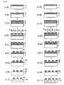
- Fig. 1 is a flow chart showing one embodiment of a patterning process according to the present invention.
- the inventors carried out extensive investigation on a composition for forming a silicon-containing resist underlayer film whose contact angle decreases only in the exposed area; and as a result, the inventors found that, when a polymer having an acid-labile group and a polymer not having this group were blended in an appropriate mixing ratio, a composition for forming a silicon-containing resist underlayer film whose contact angle decreased only in the exposed area could be obtained thereby accomplishing the present invention.
- etching selectivity with the photoresist film could be optimized so that both etching performance and patterning performance could be satisfied.
- composition of the present invention for forming a silicon-containing resist underlayer film when a silicon-containing compound containing a hydroxyl group or a carboxyl group, the groups being substituted with an acid-labile group, is mixed as the component (A) with a silicon-containing compound having excellent etching selectivity with the photoresist as the component (B), whereby localizing the component (A) on surface of the resist underlayer film, respective optimum surface contact angles during the time of the positive development and the negative development can be realized.
- the composition of the present invention for forming a silicon-containing resist underlayer film contains, as the component (A), a silicon-containing compound obtained by a hydrolysis-condensation reaction of a mixture containing, at least, one or more hydrolysable silicon compound shown by the following general formula (1) and one or more hydrolysable compound shown by the following general formula (2), R 1 m1 R 2 m2 R 3 m3 Si(OR) (4-m1-m2-m3) (1) wherein, R represents a hydrocarbon group having 1 to 6 carbon atoms; and at least one of R 1 , R 2 , and R 3 is an organic group as disclosed in claim 1, while the other is a hydrogen atom or a monovalent organic group having 1 to 30 carbon atoms.
- examples of the hydrolysable compound shown by the formula (2) include, as monomers, aluminum methoxide, aluminum ethoxide, aluminum propoxide, aluminum butoxide, aluminum amyloxide, aluminum hexyloxide, aluminum cyclopentoxide, aluminum cyclohexyloxide, aluminum allyloxide, aluminum phenoxide, aluminum methoxyethoxide, aluminum ethoxyethoxide, aluminum dipropoxyethyl-acetoacetate, aluminum dibutoxyethyl-acetoacetate, aluminum propoxy-bis-ethyl-acetoacetate, aluminum butoxy-bis-ethyl-acetoacetate, aluminum 2,4-pentanedionate, and aluminum 2,2,6,6-tetramethyl-3,5-heptanedionate.
- examples of the hydrolysable compound shown by the formula (2) include, as monomers, yttrium methoxide, yttrium ethoxide, yttrium propoxide, yttrium butoxide, yttrium amyloxide, yttrium hexyloxide, yttrium cyclopentoxide, yttrium cyclohexyloxide, yttrium allyloxide, yttrium phenoxide, yttrium methoxyethoxide, yttrium ethoxyethoxide, yttrium dipropoxyethyl-acetoacetate, yttrium dibutoxyethyl-acetoacetate, yttrium propoxy-bis-ethyl-acetoacetate, yttrium butoxy-bis-ethyl-acetoacetate, yttrium 2,4-pentaned
- examples of the hydrolysable compound shown by the formula (2) include, as monomers, germanium methoxide, germanium ethoxide, germanium propoxide, germanium butoxide, germanium amyloxide, germanium hexyloxide, germanium cyclopentoxide, germanium cyclohexyloxide, germanium allyloxide, germanium phenoxide, germanium methoxyethoxide, and germanium ethoxyethoxide.
- examples of the hydrolysable compound shown by the formula (2) include, as monomers, methoxy arsenic, ethoxy arsenic, propoxy arsenic, butoxy arsenic, and phenoxy arsenic.
- examples of the hydrolysable compound shown by the formula (2) include, as monomers, methoxy antimony, ethoxy antimony, propoxy antimony, butoxy antimony, phenoxy antimony, antimony acetate, and antimony propionate.
- examples of the compounds represented by the formula (2) include, as monomers, trimethyl phosphite, triethyl phosphite, tripropyl phosphite, and diphosphorus pentoxide.
- composition of the present invention for forming a silicon-containing resist underlayer film contains, as the component (B), a silicon-containing compound obtained by a hydrolysis-condensation reaction of a mixture containing, at least, one or more hydrolysable silicon compound shown by the following general formula (3) and one or more hydrolysable silicon compound shown by the following general formula (4).
- Component (B) is not particularly restricted, but the component preferably does not contain a hydroxyl group or a carboxyl group, the groups being substituted with an acid-labile group, R 6 m6 R 7 m7 R 8 m 8 Si(OR 9 ) (4-m6-m7-m8) (3) wherein, R 9 represents an alkyl group having 1 to 6 carbon atoms, and each R 6 , R 7 , and R 8 represents a hydrogen atom or a monovalent organic group having 1 to 30 carbon atoms.
- m6, m7, and m8 represent 0 or 1 and satisfy 1 ⁇ m6+m7+m8 ⁇ 3, Si(OR 10 ) 4 (4) wherein, R 10 represents an alkyl group having 1 to 6 carbon atoms.
- the silicon-containing compound of the present invention can be produced, by conducting hydrolytic condensation between monomers, while adopting, as an acid catalyst, one or more kinds of compounds selected from inorganic acids, aliphatic sulfonic acids, and aromatic sulfonic acids.
- Concentration at this time is preferably 0.1 to 20% by mass.
- the amount of water upon obtainment of the silicon-containing compound from these monomers by hydrolytic condensation is preferably 0.1 to 50 moles per mole of hydrolyzable substitutional groups bonded to the monomers. Addition amounts 50 moles or less are economical, due to small-sized apparatuses to be used for reactions.
- Suitable as a final solvent to be added to the silicon-containing compound solution is an alcohol-based solvent, and particularly desirable examples thereof include monoalkyl ether derivatives of: ethylene glycol, diethylene glycol, triethylene glycol, propylene glycol, and dipropylene glycol.
- Preferable examples concretely include propylene glycol monomethyl ether, ethylene glycol monomethyl ether, propylene glycol monoethyl ether, ethylene glycol monoethyl ether, propylene glycol monopropyl ether, and ethylene glycol monopropyl ether.
- the organic solvents which can be used as organic solution of monomers or which can be used as the water-containing organic solvent, are preferably water-soluble one.
- examples thereof include methanol, ethanol, 1-propanol, 2-propanol, 1-butanol, 2-butanol, 2-methyl-1-propanol, acetone, tetrahydrofuran, acetonitrile; and polyvalent alcohol condensate derivatives such as: propylene glycol monomethyl ether, ethylene glycol monomethyl ether, propylene glycol monoethyl ether, ethylene glycol monoethyl ether, propylene glycol monopropyl ether, ethylene glycol monopropyl ether, propylene glycol dimethyl ether, diethylene glycol dimethyl ether, propylene glycol monomethyl ether acetate, propylene glycol monoethyl ether acetate, and propylene glycol monopropyl ether; and mixtures thereof.
- L a H b X (5) wherein, L represents lithium, sodium, potassium, rubidium, or cesium; X represents a hydroxyl group, or a monovalent, or a divalent or higher organic acid group having 1 to 30 carbon atoms; "a" represents an integer of 1 or more, “b” represents 0 or an integer of 1 or more, and a+b represents a valency of the hydroxyl group or the organic acid group, MY (6) wherein, M represents sulfonium, iodonium, or ammonium; and Y represents a non-nucleophilic counter ion.
- Particularly preferable examples include oxalic acid, maleic acid, formic acid, acetic acid, propionic acid, and citric acid. It is possible to mixingly use two or more kinds of acids, so as to keep the stability.
- the addition amount is 0.001 to 25 parts by mass, preferably 0.01 to 15 parts by mass, and more preferably 0.1 to 5 parts by mass, relative to 100 parts by mass of the silicon contained in the composition.
- the composition may be added water.
- water When water is added thereinto, the silicon-containing compound is hydrated, so that a lithography performance may be improved.
- Amount of water in the solvent component of the composition is in the range of more than 0% by mass to less than 50% by mass, more preferably 0.3 to 30% by mass, or still more preferably 0.5 to 20% by mass. If amount of each component is too large, uniformity of a silicon-containing resist underlayer film becomes poor, whereby eye holes occur if the worst happens. On the other hand, if the amount thereof is too small, a lithography performance is deteriorated; and thus it is not desirable.
- a photoacid generator may be added.
- photoacid generators to be used for the present invention include a material described in paragraphs (0160) to (0179) of Japanese Patent Laid-Open (kokai) No. 2009-126940 .
- a surfactant as required.
- a surfactant include materials described in paragraph (0185) of Japanese Patent Laid-Open (kokai) No. 2009-126940 .
- a metal constituting the body to be processed is silicon, titanium, tungsten, hafnium, zirconium, chromium, germanium, copper, aluminum, iron, or an alloy thereof, and usable as the layer to be processed containing such a metal is Si, SiO 2 , SiN, SiON, SiOC, p-Si, ⁇ -Si, TiN, WSi, BPSG, SOG, Cr, CrO, CrON, MoSi, W, W-Si, Al, Cu, Al-Si, or the like, or various low dielectric films, or an etching stopper film therefor, for example, which can each be formed to typically have a thickness of 50 to 10,000nm, and particularly 100 to 5,000nm.
- the photoresist film is of a chemical amplification type, and is not particularly restricted as far as it can form a negative pattern by development using an organic solvent developer.
- the photoresist film is formed thereon by using a photoresist composition solution by using preferably a spin coating method, similarly to the case of the silicon-containing resist underlayer film.
- a photoresist composition solution by using preferably a spin coating method, similarly to the case of the silicon-containing resist underlayer film.
- pre-baking is carried out, preferably at 80 to 180°C and for 10 to 300 seconds. Then, this is followed by exposure, and then, the organic solvent development to obtain a negative resist pattern.
- PEB post-exposure baking
- a polycyclic skeleton may be introduced such as for example in the case of 6,6'-(9-fluorenylidene)-di(2-naphthol) novolak resin, or in addition, a polyimide resin may be selected (for example, Japanese Patent Laid-Open (kokai) No. 2004-153125 ).
- the negative-patterning process of the present invention according to the three-layer resist method as mentioned above is done as following (refer to FIG. 1 ).
- the organic underlayer film 2 is formed on the body to be processed 1 by a spin coating method ( FIG. 1 (I-A)). It is desired that the organic under layer film 2 have high etching resistance because this acts as a mask during etching of the body to be processed 1; and it is also desired that this undergo crosslinking by heat or an acid after forming by spin coating because mixing with the silicon-containing film of the upper layer is undesirable.
- the body to be processed 1 can be dry-etched with high precision by using, for example, a fluorine-based dry etching or a chlorine-based dry etching to transfer the negative pattern 1a to the body to be processed 1 ( FIG. 1 (I-I)).
- Pattern etching test negative pattern
- silicon-containing resist underlayer films Film-11 to Film-40 and Film-43 were prepared; and onto each of these silicon-containing resist underlayer films was applied the ArF resist solution for the negative development shown in Table 12 (PR-3 and PR-4), and then baked at 100°C for 60 seconds to form the photoresist film having film thickness of 100 nm.
- Onto the photoresist film was applied the immersion top coat shown in Table 10 (TC-1), and then baked at 90°C for 60 seconds to form the top coat having film thickness of 50 nm (E xamples 5-1 to 5-20, 5-29 to 5-30, and Comparative Example 5-1 ).
Landscapes
- Chemical & Material Sciences (AREA)
- General Physics & Mathematics (AREA)
- Physics & Mathematics (AREA)
- Chemical Kinetics & Catalysis (AREA)
- Engineering & Computer Science (AREA)
- Organic Chemistry (AREA)
- Materials Engineering (AREA)
- Life Sciences & Earth Sciences (AREA)
- Structural Engineering (AREA)
- Wood Science & Technology (AREA)
- Architecture (AREA)
- Health & Medical Sciences (AREA)
- Medicinal Chemistry (AREA)
- Polymers & Plastics (AREA)
- Materials For Photolithography (AREA)
- Photosensitive Polymer And Photoresist Processing (AREA)
- Polymers With Sulfur, Phosphorus Or Metals In The Main Chain (AREA)
Claims (10)
- Zusammensetzung zum Bilden eines Silizium-enthaltenden Resistunterschichtfilms umfassend:(A) eine Silizium-enthaltende Verbindung, erhalten durch eine Hydrolyse-Kondensationsreaktion einer Mischung enthaltend, mindestens, eine oder mehrere durch die folgende allgemeine Formel (1) gezeigte hydrolysierbare Siliziumverbindung(en) und eine oder mehrere durch die folgende allgemeine Formel (2) gezeigte hydrolysierbare Verbindung(en),
R1 m1R2 m2R3 m3Si(OR)(4-m1-m2-m3) (1)
wobei R eine Kohlenwasserstoffgruppe mit 1 bis 6 Kohlenstoffatomen darstellt; mindestens eine von R1, R2 und R3 eine aus den durch die folgenden Strukturformeln ausgewählte organische Gruppe ist, während die andere ein Wasserstoffatom oder eine monovalente organische Gruppe mit 1 bis 30 Kohlenstoffatomen ist; und m1, m2 und m3 0 oder 1 darstellen und 1≤m1+m2+m3≤3 erfüllen;



















wobei R4 und R5 eine organische Gruppe mit 1 bis 30 Kohlenstoffatomen darstellen und m4+m5 die gleiche Zahl wie die durch die Valenz von U bestimmte Zahl ist; m4 und m5 eine Ganzzahl von 0 oder mehr darstellen; und das U ein Element, das zu den Gruppen von III, IV oder V des Periodensystems, ausgenommen Kunststoff und Silizium, ist;(B) eine Silizium-enthaltende Verbindung, erhalten durch eine Hydrolyse-Kondensationsreaktion einer Mischung enthaltend, mindestens, eine oder mehrere durch die folgende allgemeine Formel (3) gezeigte hydrolysierbare Siliziumverbindung(en) und eine oder mehrere durch die folgende allgemeine Formel (4) gezeigte hydrolysierbare Siliziumverbindung(en),
R6 m6R7 m7R8 m8Si(OR9)(4-m6-m7-m8) (3)
wobei R9 eine Alkylgruppe mit 1 bis 6 Kohlenstoffatomen darstellt, und jeder R6, R7 und R8 ein Wasserstoffatom oder eine monovalente organische Gruppe mit 1 bis 30 Kohlenstoffatomen darstellt; und m6, m7 und m8 0 oder 1 darstellen und 1≤m6+m7+m8≤3 erfüllen; und
Si(OR10)4 (4)
wobei R10 eine Alkylgruppe mit 1 bis 6 Kohlenstoffatomen darstellt;
und das Masseverhältnis der Komponente (A) zu der Komponente (B) (B)/(A)≥1 erfüllt,
und der konstituierenden Einheiten, abgeleitet aus der allgemeinen Formel (3) und der allgemeinen Formel (4) in der Komponente (B), das Molverhältnis der konstituierenden Einheit, abgeleitet aus der allgemeinen Formel (4), 50 Mol-% oder mehr beträgt. - Zusammensetzung zum Bilden eines Silizium-enthaltenden Resistunterschichtfilms nach Anspruch 1,
wobei das U der allgemeinen Formel (2) ein Beliebiges von Bor, Aluminium, Gallium, Yttrium, Germanium, Titan, Zirkonium, Hafnium, Bismuth, Zinn, Phosphor, Vanadium, Arsen, Antimon, Niob und Tantal ist. - Strukturierungsverfahren, wobei ein organischer Unterschichtfilm auf einem zu prozessierenden Körper durch Verwenden einer Applikationstyp-Zusammensetzung für den organischen Unterschichtfilm gebildet wird, auf diesem organischen Unterschichtfilm ein Silizium-enthaltender Resistunterschichtfilm durch Verwenden der Zusammensetzung zum Bilden des Silizium-enthaltenden Resistunterschichtfilms gemäß Anspruch 1 oder 2 gebildet wird,
auf diesem Silizium-enthaltenden Resistunterschichtfilm ein Photoresistfilm durch Verwenden einer chemisch amplifizierten Resist-Zusammensetzung gebildet wird, der Photoresistfilm einem Hochenergiestrahl nach Hitzebehandlung ausgesetzt wird, eine positive Struktur durch Auflösen einer ausgesetzten Fläche des Photoresistfilms durch Verwenden eines alkalischen Entwicklers gebildet wird, Strukturtransfer auf den Silizium-enthaltenden Resistunterschichtfilm durch Trockenätzen unter Verwendung des Photoresistfilms mit der positiven Struktur als einer Maske durchgeführt wird, Strukturtransfer auf den organischen Unterschichtfilm durch Trockenätzen unter Verwendung des Silizium-enthaltenden Resistunterschichtfilms mit der transferierten Struktur als einer Maske durchgeführt wird, und dann Strukturtransfer auf den zu prozessierenden Körper durch Trockenätzen unter Verwendung des organischen Unterschichtfilms mit der transferierten Struktur als einer Maske durchgeführt wird. - Strukturierungsverfahren, wobei eine organische Hartmaske, die hauptsächlich Kohlenstoff umfasst, auf einem zu prozessierenden Körper durch ein CVD-Verfahren gebildet wird, auf dieser organischen Hartmaske ein Silizium-enthaltender Resistunterschichtfilm durch Verwenden der Zusammensetzung zum Bilden des Siliziumenthaltenden Resistunterschichtfilms gemäß Anspruch 1 oder 2 gebildet wird, auf diesem Silizium-enthaltenden Resistunterschichtfilm ein Photoresistfilm unter Verwendung einer chemisch amplifizierten Resist-Zusammensetzung gebildet wird, der Photoresistfilm einem Hochenergiestrahl nach Hitzebehandlung ausgesetzt wird, eine positive Struktur durch Auflösen einer ausgesetzten Fläche des Photoresistfilms unter Verwendung eines alkalischen Entwicklers gebildet wird, Strukturtransfer auf den Silizium-enthaltenden Resistunterschichtfilm durch Trockenätzen unter Verwendung des Photoresistfilms mit der positiven Struktur als einer Maske durchgeführt wird, Strukturtransfer auf die organische Hartmaske durch Trockenätzen unter Verwendung des Silizium-enthaltenden Resistunterschichtfilms mit der transferierten Struktur als einer Maske durchgeführt wird, und dann Strukturtransfer auf den zu prozessierenden Körper durch Trockenätzen unter Verwendung der organischen Hartmaske mit der transferierten Struktur als einer Maske durchgeführt wird.
- Strukturierungsverfahren nach Anspruch 3 oder 4,
wobei, während Photobelichtung des Photoresistfilms, eine Veränderung des Kontaktwinkels in einem Teil des Silizium-enthaltenden Resistunterschichtfilms, der einer nicht ausgesetzten Fläche des ausgesetzten Photoresistfilms entspricht, 10 Grad oder weniger, verglichen zu vor der Photobelichtung, beträgt. - Strukturierungsverfahren, wobei ein organischer Unterschichtfilm auf einem zu prozessierenden Körper durch Verwenden einer Applikationstyp-Zusammensetzung für den organische Unterschichtfilm gebildet wird, auf diesem organischen Unterschichtfilm ein Silizium-enthaltender Resistunterschichtfilm durch Verwenden der Zusammensetzung zum Bilden des Silizium-enthaltenden Resistunterschichtfilms gemäß Anspruch 1 oder 2 gebildet wird,
auf diesem Silizium-enthaltenden Resistunterschichtfilm ein Photoresistfilm durch Verwenden einer chemisch amplifizierten Resist-Zusammensetzung gebildet wird, der Photoresistfilm einem Hochenergiestrahl nach Hitzebehandlung ausgesetzt wird, eine negative Struktur durch Auflösen einer nicht ausgesetzten Fläche des Photoresistfilms durch Verwenden eines organischen Lösemittelentwicklers gebildet wird, Strukturtransfer auf den Silizium-enthaltenden Resistunterschichtfilm durch Trockenätzen unter Verwendung des Photoresistfilms mit der negativen Struktur als einer Maske durchgeführt wird, Strukturtransfer auf den organischen Unterschichtfilm durch Trockenätzen unter Verwendung des Silizium-enthaltenden Resistunterschichtfilms mit der transferierten Struktur als einer Maske durchgeführt wird, und dann Strukturtransfer auf den zu prozessierenden Körper durch Trockenätzen unter Verwendung des organischen Unterschichtfilms mit der transferierten Struktur als einer Maske durchgeführt wird. - Strukturierungsverfahren, wobei eine organische Hartmaske, die hauptsächlich Kohlenstoff umfasst, auf einem zu verarbeitenden Körper durch ein CVD-Verfahren gebildet wird, auf dieser organischen Hartmaske ein Silizium-enthaltender Resistunterschichtfilm durch Verwenden der Zusammensetzung zum Bilden des Silizium-enthaltenden Resistunterschichtfilms gemäß Anspruch 1 oder 2 gebildet wird, auf diesem Silizium-enthaltenden Resistunterschichtfilm ein Photoresistfilm unter Verwendung einer chemisch amplifizierten Resist-Zusammensetzung gebildet wird, der Photoresistfilm einem Hochenergiestrahl nach Hitzebehandlung ausgesetzt wird, eine negative Struktur durch Auflösen einer nicht ausgesetzten Fläche des Photoresistfilms durch Verwenden eines organischen Lösemittelentwicklers gebildet wird, Strukturtransfer auf den Silizium-enthaltenden Resistunterschichtfilm durch Trockenätzen unter Verwendung des Photoresistfilms mit der negativen Struktur als einer Maske durchgeführt wird, Strukturtransfer auf die organische Hartmaske durch Trockenätzen unter Verwendung des Silizium-enthaltenden Resistunterschichtfilms mit der transferierten Struktur als einer Maske durchgeführt wird, und dann Strukturtransfer auf den zu prozessierenden Körper durch Trockenätzen unter Verwendung der organischen Hartmaske mit der transferierten Struktur als einer Maske durchgeführt wird.
- Strukturierungsverfahren nach Anspruch 6 oder 7,
wobei, während Photobelichtung des Photoresistfilms, der Kontaktwinkel eines Teils des Silizium-enthaltenden Resistunterschichtfilms, der einer ausgesetzten Fläche des ausgesetzten Photoresistfilms entspricht, um 10 Grad oder mehr nach Photobelichtung, verglichen zu vor der Photobelichtung, verringert wird. - Strukturierungsverfahren nach einem beliebigen der Ansprüche 3 bis 8, wobei der zu prozessierende Körper ein Substrat für eine Halbleitervorrichtung ist, oder das Substrat für eine Halbleitervorrichtung beschichtet ist, als eine zu prozessierende Schicht, mit einem Beliebigen von einem Metallfilm, einem Metallcarbidfilm, einem Metalloxidfilm, einem Metallnitridfilm, einem Metalloxycarbidfilm und einem Metalloxynitridfilm.
- Strukturierungsverfahren nach einem beliebigen der Ansprüche 3 bis 9, wobei das Metall, welches den zu prozessierenden Körper bildet, Silizium, Titan, Wolfram, Hafnium, Zirkonium, Chrom, Germanium, Kupfer, Aluminium, Eisen oder eine Legierung von diesen Metallen ist.
Applications Claiming Priority (2)
| Application Number | Priority Date | Filing Date | Title |
|---|---|---|---|
| JP2011142657 | 2011-06-28 | ||
| JP2011220708A JP5650086B2 (ja) | 2011-06-28 | 2011-10-05 | レジスト下層膜形成用組成物、及びパターン形成方法 |
Publications (2)
| Publication Number | Publication Date |
|---|---|
| EP2540780A1 EP2540780A1 (de) | 2013-01-02 |
| EP2540780B1 true EP2540780B1 (de) | 2016-07-20 |
Family
ID=46396974
Family Applications (1)
| Application Number | Title | Priority Date | Filing Date |
|---|---|---|---|
| EP12004626.3A Active EP2540780B1 (de) | 2011-06-28 | 2012-06-20 | Zusammensetzung zur Bildung einer Resistunterschichtfolie, und Strukturierungsverfahren |
Country Status (5)
| Country | Link |
|---|---|
| US (1) | US8951917B2 (de) |
| EP (1) | EP2540780B1 (de) |
| JP (1) | JP5650086B2 (de) |
| KR (1) | KR101735856B1 (de) |
| TW (1) | TWI461852B (de) |
Families Citing this family (51)
| Publication number | Priority date | Publication date | Assignee | Title |
|---|---|---|---|---|
| US9176377B2 (en) | 2010-06-01 | 2015-11-03 | Inpria Corporation | Patterned inorganic layers, radiation based patterning compositions and corresponding methods |
| JP5785121B2 (ja) * | 2011-04-28 | 2015-09-24 | 信越化学工業株式会社 | パターン形成方法 |
| JP5650086B2 (ja) | 2011-06-28 | 2015-01-07 | 信越化学工業株式会社 | レジスト下層膜形成用組成物、及びパターン形成方法 |
| JP5771570B2 (ja) * | 2011-06-30 | 2015-09-02 | 富士フイルム株式会社 | パターン形成方法、積層レジストパターン、及び、電子デバイスの製造方法 |
| JP5999372B2 (ja) * | 2011-07-20 | 2016-09-28 | 日産化学工業株式会社 | チタン及びシリコン含有リソグラフィー用薄膜形成組成物 |
| JP5453361B2 (ja) * | 2011-08-17 | 2014-03-26 | 信越化学工業株式会社 | ケイ素含有レジスト下層膜形成用組成物、及びパターン形成方法 |
| WO2013051558A1 (ja) * | 2011-10-06 | 2013-04-11 | 日産化学工業株式会社 | ケイ素含有euvレジスト下層膜形成組成物 |
| JP5894762B2 (ja) * | 2011-10-27 | 2016-03-30 | 富士フイルム株式会社 | パターン形成方法、及び電子デバイスの製造方法 |
| JP5746005B2 (ja) * | 2011-11-29 | 2015-07-08 | 信越化学工業株式会社 | ケイ素含有レジスト下層膜形成用組成物及びパターン形成方法 |
| US9214345B2 (en) | 2012-02-09 | 2015-12-15 | Nissan Chemical Industries, Ltd. | Film-forming composition and ion implantation method |
| JP5882776B2 (ja) * | 2012-02-14 | 2016-03-09 | 信越化学工業株式会社 | レジスト下層膜形成用組成物、及びパターン形成方法 |
| JP5739360B2 (ja) | 2012-02-14 | 2015-06-24 | 信越化学工業株式会社 | ケイ素含有レジスト下層膜形成用組成物、及びパターン形成方法 |
| EP2832807A4 (de) * | 2012-03-27 | 2015-10-21 | Nissan Chemical Ind Ltd | Unterschichtfilmbildende zusammensetzung für selbstaufbauende filme |
| JP5833492B2 (ja) * | 2012-04-23 | 2015-12-16 | 信越化学工業株式会社 | ケイ素化合物、ポリシロキサン化合物、これを含むレジスト下層膜形成用組成物及びパターン形成方法 |
| JP5642731B2 (ja) | 2012-04-27 | 2014-12-17 | 信越化学工業株式会社 | パターン形成方法 |
| JP5710546B2 (ja) | 2012-04-27 | 2015-04-30 | 信越化学工業株式会社 | パターン形成方法 |
| JP6060577B2 (ja) * | 2012-09-13 | 2017-01-18 | Jsr株式会社 | ネガ型レジストパターン形成方法 |
| US8828744B2 (en) * | 2012-09-24 | 2014-09-09 | Lam Research Corporation | Method for etching with controlled wiggling |
| JP5859466B2 (ja) * | 2013-01-08 | 2016-02-10 | 信越化学工業株式会社 | チタン含有レジスト下層膜形成用組成物及びパターン形成方法 |
| JP5756134B2 (ja) | 2013-01-08 | 2015-07-29 | 信越化学工業株式会社 | 金属酸化物含有膜形成用組成物及びパターン形成方法 |
| JP5830044B2 (ja) | 2013-02-15 | 2015-12-09 | 信越化学工業株式会社 | レジスト下層膜形成用組成物及びパターン形成方法 |
| US8759220B1 (en) * | 2013-02-28 | 2014-06-24 | Shin-Etsu Chemical Co., Ltd. | Patterning process |
| JP5830048B2 (ja) * | 2013-03-15 | 2015-12-09 | 信越化学工業株式会社 | チタン含有レジスト下層膜形成用組成物及びパターン形成方法 |
| JP6215777B2 (ja) * | 2013-06-27 | 2017-10-18 | 信越化学工業株式会社 | 塗布型bpsg膜形成用組成物、該組成物で膜を形成した基板、及び前記組成物を用いたパターン形成方法 |
| US9310684B2 (en) | 2013-08-22 | 2016-04-12 | Inpria Corporation | Organometallic solution based high resolution patterning compositions |
| JP2015182978A (ja) * | 2014-03-25 | 2015-10-22 | 信越化学工業株式会社 | 有機ケイ素化合物及び接着性組成物並びに物品 |
| US10739673B2 (en) | 2014-06-20 | 2020-08-11 | Taiwan Semiconductor Manufacturing Company Limited | Preparing patterned neutral layers and structures prepared using the same |
| US11815815B2 (en) * | 2014-11-19 | 2023-11-14 | Nissan Chemical Industries, Ltd. | Composition for forming silicon-containing resist underlayer film removable by wet process |
| KR102374049B1 (ko) | 2015-06-02 | 2022-03-14 | 삼성전자주식회사 | 포토레지스트를 이용한 패턴 형성 방법 |
| KR20170016107A (ko) | 2015-08-03 | 2017-02-13 | 삼성전자주식회사 | 반도체 장치 제조 방법 |
| CN108291031B (zh) | 2015-11-26 | 2021-06-15 | 东丽株式会社 | 聚金属氧烷、其制造方法、其组合物、固化膜和其制造方法以及具备其的构件和电子部件 |
| US10007184B2 (en) | 2016-09-01 | 2018-06-26 | Rohm And Haas Electronic Materials Llc | Silicon-containing underlayers |
| US10114288B2 (en) * | 2016-09-01 | 2018-10-30 | Rohm And Haas Electronic Materials Llc | Silicon-containing underlayers |
| JP7024744B2 (ja) | 2018-02-22 | 2022-02-24 | 信越化学工業株式会社 | レジスト材料及びこれを用いたパターン形成方法 |
| CN111902774B (zh) * | 2018-03-19 | 2023-10-31 | 日产化学株式会社 | 包含硝酸和被保护了的苯酚基的含硅抗蚀剂下层膜形成用组合物 |
| KR102307977B1 (ko) | 2018-07-31 | 2021-09-30 | 삼성에스디아이 주식회사 | 반도체 레지스트용 조성물 및 이를 이용한 패턴 형성 방법 |
| US11092890B2 (en) | 2018-07-31 | 2021-08-17 | Samsung Sdi Co., Ltd. | Semiconductor resist composition, and method of forming patterns using the composition |
| US11092889B2 (en) | 2018-07-31 | 2021-08-17 | Samsung Sdi Co., Ltd. | Semiconductor resist composition, and method of forming patterns using the composition |
| JP7241486B2 (ja) * | 2018-08-21 | 2023-03-17 | 東京エレクトロン株式会社 | マスクの形成方法 |
| JP7357505B2 (ja) * | 2018-11-21 | 2023-10-06 | 信越化学工業株式会社 | ヨウ素含有熱硬化性ケイ素含有材料、これを含むeuvリソグラフィー用レジスト下層膜形成用組成物、及びパターン形成方法 |
| JP7307005B2 (ja) | 2019-04-26 | 2023-07-11 | 信越化学工業株式会社 | 硬化触媒の拡散距離を測定する方法 |
| US11609494B2 (en) | 2019-04-30 | 2023-03-21 | Samsung Sdi Co., Ltd. | Semiconductor photoresist composition and method of forming patterns using the composition |
| JP7368324B2 (ja) | 2019-07-23 | 2023-10-24 | 信越化学工業株式会社 | ケイ素含有レジスト下層膜形成用組成物及びパターン形成方法 |
| KR102446362B1 (ko) | 2019-10-15 | 2022-09-21 | 삼성에스디아이 주식회사 | 반도체 포토 레지스트용 조성물 및 이를 이용한 패턴 형성 방법 |
| JP7402715B2 (ja) * | 2020-03-06 | 2023-12-21 | 東京エレクトロン株式会社 | ウエハを処理する方法 |
| KR102573327B1 (ko) | 2020-04-02 | 2023-08-30 | 삼성에스디아이 주식회사 | 반도체 포토레지스트용 조성물 및 이를 이용한 패턴 형성 방법 |
| KR102619719B1 (ko) | 2020-05-12 | 2023-12-28 | 삼성에스디아이 주식회사 | 반도체 포토레지스트용 조성물 및 이를 이용한 패턴 형성 방법 |
| KR102586112B1 (ko) | 2020-09-14 | 2023-10-05 | 삼성에스디아이 주식회사 | 반도체 포토레지스트용 조성물 및 이를 이용한 패턴 형성 방법 |
| KR102598259B1 (ko) | 2020-12-18 | 2023-11-02 | 삼성에스디아이 주식회사 | 반도체 포토레지스트용 조성물 및 이를 이용한 패턴 형성 방법 |
| KR102690557B1 (ko) | 2020-12-18 | 2024-07-30 | 삼성에스디아이 주식회사 | 반도체 포토레지스트용 조성물, 이의 제조 방법 및 이를 이용한 패턴 형성 방법 |
| KR20240051105A (ko) * | 2021-08-31 | 2024-04-19 | 미쯔비시 가스 케미칼 컴파니, 인코포레이티드 | 스핀온 카본막 형성용 조성물, 스핀온 카본막 형성용 조성물의 제조방법, 리소그래피용 하층막, 레지스트패턴 형성방법, 및 회로패턴 형성방법 |
Family Cites Families (43)
| Publication number | Priority date | Publication date | Assignee | Title |
|---|---|---|---|---|
| US4510136A (en) | 1981-06-24 | 1985-04-09 | E. I. Du Pont De Nemours And Company | Fungicidal 1,2,4-triazole derivatives |
| JPH07183194A (ja) | 1993-12-24 | 1995-07-21 | Sony Corp | 多層レジストパターン形成方法 |
| JPH07181688A (ja) | 1993-12-24 | 1995-07-21 | Sony Corp | 多層レジストパターン形成方法 |
| JP2862786B2 (ja) | 1994-01-27 | 1999-03-03 | 信越化学工業株式会社 | ポリエステル−シリコーン共重合体及びそれを用いた被覆組成物 |
| JP3324360B2 (ja) * | 1995-09-25 | 2002-09-17 | 信越化学工業株式会社 | ポリシロキサン化合物及びポジ型レジスト材料 |
| JPH11258813A (ja) | 1998-03-13 | 1999-09-24 | Jsr Corp | 反射防止膜形成用組成物および反射防止膜 |
| JP2000053921A (ja) | 1998-08-12 | 2000-02-22 | Sumitomo Chem Co Ltd | 反射防止被膜形成組成物 |
| JP4320883B2 (ja) * | 1999-12-13 | 2009-08-26 | Jsr株式会社 | レジスト下層膜用組成物 |
| ATE280188T1 (de) | 1999-12-22 | 2004-11-15 | Basell Poliolefine Spa | Alpha-olefin enthaltendes polymerisationskatalysatorsystem, das ein aromatisches silan enthält |
| US6531260B2 (en) | 2000-04-07 | 2003-03-11 | Jsr Corporation | Polysiloxane, method of manufacturing same, silicon-containing alicyclic compound, and radiation-sensitive resin composition |
| US6420088B1 (en) | 2000-06-23 | 2002-07-16 | International Business Machines Corporation | Antireflective silicon-containing compositions as hardmask layer |
| US6740469B2 (en) | 2002-06-25 | 2004-05-25 | Brewer Science Inc. | Developer-soluble metal alkoxide coatings for microelectronic applications |
| US6872506B2 (en) | 2002-06-25 | 2005-03-29 | Brewer Science Inc. | Wet-developable anti-reflective compositions |
| AU2002329596A1 (en) | 2002-07-11 | 2004-02-02 | International Business Machines Corporation | Antireflective silicon-containing compositions as hardmask layer |
| JP2004153125A (ja) | 2002-10-31 | 2004-05-27 | Fujitsu Ltd | 加工用マスクの形成方法及び半導体装置の製造方法 |
| JP5124077B2 (ja) * | 2003-03-03 | 2013-01-23 | ローム・アンド・ハース・エレクトロニック・マテリアルズ,エル.エル.シー. | ポリマー、およびそれを含むフォトレジスト |
| JP2004354417A (ja) | 2003-05-27 | 2004-12-16 | Shin Etsu Chem Co Ltd | ポジ型レジスト材料並びにこれを用いたパターン形成方法 |
| JP4359467B2 (ja) | 2003-08-28 | 2009-11-04 | 信越化学工業株式会社 | 新規スルホニルジアゾメタン化合物、光酸発生剤、並びにそれを用いたレジスト材料及びパターン形成方法。 |
| US7303855B2 (en) | 2003-10-03 | 2007-12-04 | Shin-Etsu Chemical Co., Ltd. | Photoresist undercoat-forming material and patterning process |
| JP4355943B2 (ja) | 2003-10-03 | 2009-11-04 | 信越化学工業株式会社 | フォトレジスト下層膜形成材料及びパターン形成方法 |
| JP2005173552A (ja) | 2003-11-20 | 2005-06-30 | Tokyo Ohka Kogyo Co Ltd | リソグラフィー用下層膜形成材料およびこれを用いた配線形成方法 |
| JP4539131B2 (ja) | 2004-03-16 | 2010-09-08 | 住友化学株式会社 | 有機ケイ素系化合物、及びその製造方法 |
| JP4488215B2 (ja) | 2004-08-19 | 2010-06-23 | 信越化学工業株式会社 | レジスト組成物並びにこれを用いたパターン形成方法 |
| JP4552132B2 (ja) | 2005-03-10 | 2010-09-29 | ラサ工業株式会社 | 多層レジスト中間層形成用塗布液及びこれを用いたパターン形成方法 |
| JP4583237B2 (ja) | 2005-05-16 | 2010-11-17 | 東京応化工業株式会社 | 反射防止膜形成用組成物、および配線形成方法 |
| JP4553835B2 (ja) | 2005-12-14 | 2010-09-29 | 信越化学工業株式会社 | 反射防止膜材料、及びこれを用いたパターン形成方法、基板 |
| JP4659678B2 (ja) | 2005-12-27 | 2011-03-30 | 信越化学工業株式会社 | フォトレジスト下層膜形成材料及びパターン形成方法 |
| JP4638380B2 (ja) * | 2006-01-27 | 2011-02-23 | 信越化学工業株式会社 | 反射防止膜材料、反射防止膜を有する基板及びパターン形成方法 |
| JP4842844B2 (ja) | 2006-04-04 | 2011-12-21 | 信越化学工業株式会社 | レジスト材料及びこれを用いたパターン形成方法 |
| US7771913B2 (en) | 2006-04-04 | 2010-08-10 | Shin-Etsu Chemical Co., Ltd. | Resist composition and patterning process using the same |
| JP4716037B2 (ja) | 2006-04-11 | 2011-07-06 | 信越化学工業株式会社 | ケイ素含有膜形成用組成物、ケイ素含有膜、ケイ素含有膜形成基板及びこれを用いたパターン形成方法 |
| EP1845132B8 (de) | 2006-04-11 | 2009-04-01 | Shin-Etsu Chemical Co., Ltd. | Siliziumhaltige, folienbildende Zusammensetzung, siliziumhaltige Folie, siliziumhaltiges, folientragendes Substrat und Strukturierungsverfahren |
| US7855043B2 (en) * | 2006-06-16 | 2010-12-21 | Shin-Etsu Chemical Co., Ltd. | Silicon-containing film-forming composition, silicon-containing film, silicon-containing film-bearing substrate, and patterning method |
| WO2008081789A1 (ja) | 2006-12-25 | 2008-07-10 | Chugoku Marine Paints, Ltd. | 硬化性組成物、防汚塗料組成物、防汚塗膜、防汚塗膜付き基材および基材の防汚方法 |
| US8034547B2 (en) | 2007-04-13 | 2011-10-11 | Fujifilm Corporation | Pattern forming method, resist composition to be used in the pattern forming method, negative developing solution to be used in the pattern forming method and rinsing solution for negative development to be used in the pattern forming method |
| JP5002379B2 (ja) | 2007-04-13 | 2012-08-15 | 富士フイルム株式会社 | パターン形成方法 |
| JP4982288B2 (ja) | 2007-04-13 | 2012-07-25 | 富士フイルム株式会社 | パターン形成方法 |
| KR100990106B1 (ko) | 2007-04-13 | 2010-10-29 | 후지필름 가부시키가이샤 | 패턴형성방법, 이 패턴형성방법에 사용되는 레지스트 조성물, 현상액 및 린스액 |
| JP4793592B2 (ja) | 2007-11-22 | 2011-10-12 | 信越化学工業株式会社 | 金属酸化物含有膜形成用組成物、金属酸化物含有膜、金属酸化物含有膜形成基板及びこれを用いたパターン形成方法 |
| JP5015891B2 (ja) | 2008-10-02 | 2012-08-29 | 信越化学工業株式会社 | 金属酸化物含有膜形成用組成物、金属酸化物含有膜形成基板及びパターン形成方法 |
| KR101847382B1 (ko) | 2010-02-25 | 2018-04-10 | 닛산 가가쿠 고교 가부시키 가이샤 | 아믹산을 포함하는 실리콘 함유 레지스트 하층막 형성 조성물 |
| JP5785121B2 (ja) * | 2011-04-28 | 2015-09-24 | 信越化学工業株式会社 | パターン形成方法 |
| JP5650086B2 (ja) | 2011-06-28 | 2015-01-07 | 信越化学工業株式会社 | レジスト下層膜形成用組成物、及びパターン形成方法 |
-
2011
- 2011-10-05 JP JP2011220708A patent/JP5650086B2/ja active Active
-
2012
- 2012-06-15 US US13/524,669 patent/US8951917B2/en active Active
- 2012-06-20 EP EP12004626.3A patent/EP2540780B1/de active Active
- 2012-06-27 TW TW101123072A patent/TWI461852B/zh active
- 2012-06-27 KR KR1020120069106A patent/KR101735856B1/ko active Active
Also Published As
| Publication number | Publication date |
|---|---|
| JP5650086B2 (ja) | 2015-01-07 |
| KR20130002275A (ko) | 2013-01-07 |
| TW201305737A (zh) | 2013-02-01 |
| TWI461852B (zh) | 2014-11-21 |
| KR101735856B1 (ko) | 2017-05-15 |
| JP2013033187A (ja) | 2013-02-14 |
| US20130005150A1 (en) | 2013-01-03 |
| EP2540780A1 (de) | 2013-01-02 |
| US8951917B2 (en) | 2015-02-10 |
Similar Documents
| Publication | Publication Date | Title |
|---|---|---|
| EP2540780B1 (de) | Zusammensetzung zur Bildung einer Resistunterschichtfolie, und Strukturierungsverfahren | |
| EP2560049B1 (de) | Zusammensetzung zur Bildung einer siliciumhaltigen Resistunterschichtfolie, und Strukturierungsverfahren damit | |
| EP2500775B1 (de) | Strukturierungsverfahren und zusammensetzung zur bildung von siliciumhaltigem film dafür | |
| US9069247B2 (en) | Silicon-containing surface modifier, resist lower layer film-forming composition containing the same, and patterning process | |
| EP2518562B1 (de) | Strukturierungsverfahren | |
| KR101737667B1 (ko) | 규소 함유 표면개질제, 이것을 포함하는 레지스트 하층막 형성용 조성물 및 패턴 형성 방법 | |
| US8697330B2 (en) | Composition for forming a silicon-containing antireflection film, substrate having the silicon-containing antireflection film from the composition and patterning process using the same | |
| JP5746005B2 (ja) | ケイ素含有レジスト下層膜形成用組成物及びパターン形成方法 | |
| KR101767692B1 (ko) | 규소 함유 레지스트 하층막 형성용 조성물 및 패턴 형성 방법 | |
| JP5830041B2 (ja) | ポリシロキサン含有レジスト下層膜形成用組成物、及びこれを用いたパターン形成方法 | |
| US20140193975A1 (en) | Composition for forming titanium-containing resist underlayer film and patterning process | |
| US9624356B2 (en) | Ultraviolet absorber, composition for forming a resist under layer film, and patterning process | |
| US20250166999A1 (en) | Patterning Process |
Legal Events
| Date | Code | Title | Description |
|---|---|---|---|
| PUAI | Public reference made under article 153(3) epc to a published international application that has entered the european phase |
Free format text: ORIGINAL CODE: 0009012 |
|
| AK | Designated contracting states |
Kind code of ref document: A1 Designated state(s): AL AT BE BG CH CY CZ DE DK EE ES FI FR GB GR HR HU IE IS IT LI LT LU LV MC MK MT NL NO PL PT RO RS SE SI SK SM TR |
|
| AX | Request for extension of the european patent |
Extension state: BA ME |
|
| 17P | Request for examination filed |
Effective date: 20130624 |
|
| RBV | Designated contracting states (corrected) |
Designated state(s): AL AT BE BG CH CY CZ DE DK EE ES FI FR GB GR HR HU IE IS IT LI LT LU LV MC MK MT NL NO PL PT RO RS SE SI SK SM TR |
|
| 17Q | First examination report despatched |
Effective date: 20140723 |
|
| GRAP | Despatch of communication of intention to grant a patent |
Free format text: ORIGINAL CODE: EPIDOSNIGR1 |
|
| INTG | Intention to grant announced |
Effective date: 20151222 |
|
| RIN1 | Information on inventor provided before grant (corrected) |
Inventor name: OGIHARA, TSUTOMU Inventor name: YAGIHASHI, FUJIO Inventor name: YANO, TOSHIHARU Inventor name: UEDA, TAKAFUMI |
|
| GRAS | Grant fee paid |
Free format text: ORIGINAL CODE: EPIDOSNIGR3 |
|
| GRAA | (expected) grant |
Free format text: ORIGINAL CODE: 0009210 |
|
| RIN1 | Information on inventor provided before grant (corrected) |
Inventor name: OGIHARA, TSUTOMU Inventor name: UEDA, TAKAFUMI Inventor name: YAGIHASHI, FUJIO Inventor name: YANO, TOSHIHARU |
|
| AK | Designated contracting states |
Kind code of ref document: B1 Designated state(s): AL AT BE BG CH CY CZ DE DK EE ES FI FR GB GR HR HU IE IS IT LI LT LU LV MC MK MT NL NO PL PT RO RS SE SI SK SM TR |
|
| REG | Reference to a national code |
Ref country code: GB Ref legal event code: FG4D |
|
| REG | Reference to a national code |
Ref country code: CH Ref legal event code: EP |
|
| REG | Reference to a national code |
Ref country code: IE Ref legal event code: FG4D |
|
| REG | Reference to a national code |
Ref country code: AT Ref legal event code: REF Ref document number: 814075 Country of ref document: AT Kind code of ref document: T Effective date: 20160815 |
|
| REG | Reference to a national code |
Ref country code: DE Ref legal event code: R096 Ref document number: 602012020591 Country of ref document: DE |
|
| REG | Reference to a national code |
Ref country code: LT Ref legal event code: MG4D |
|
| REG | Reference to a national code |
Ref country code: NL Ref legal event code: MP Effective date: 20160720 |
|
| REG | Reference to a national code |
Ref country code: AT Ref legal event code: MK05 Ref document number: 814075 Country of ref document: AT Kind code of ref document: T Effective date: 20160720 |
|
| PG25 | Lapsed in a contracting state [announced via postgrant information from national office to epo] |
Ref country code: FI Free format text: LAPSE BECAUSE OF FAILURE TO SUBMIT A TRANSLATION OF THE DESCRIPTION OR TO PAY THE FEE WITHIN THE PRESCRIBED TIME-LIMIT Effective date: 20160720 Ref country code: LT Free format text: LAPSE BECAUSE OF FAILURE TO SUBMIT A TRANSLATION OF THE DESCRIPTION OR TO PAY THE FEE WITHIN THE PRESCRIBED TIME-LIMIT Effective date: 20160720 Ref country code: RS Free format text: LAPSE BECAUSE OF FAILURE TO SUBMIT A TRANSLATION OF THE DESCRIPTION OR TO PAY THE FEE WITHIN THE PRESCRIBED TIME-LIMIT Effective date: 20160720 Ref country code: IS Free format text: LAPSE BECAUSE OF FAILURE TO SUBMIT A TRANSLATION OF THE DESCRIPTION OR TO PAY THE FEE WITHIN THE PRESCRIBED TIME-LIMIT Effective date: 20161120 Ref country code: NO Free format text: LAPSE BECAUSE OF FAILURE TO SUBMIT A TRANSLATION OF THE DESCRIPTION OR TO PAY THE FEE WITHIN THE PRESCRIBED TIME-LIMIT Effective date: 20161020 Ref country code: IT Free format text: LAPSE BECAUSE OF FAILURE TO SUBMIT A TRANSLATION OF THE DESCRIPTION OR TO PAY THE FEE WITHIN THE PRESCRIBED TIME-LIMIT Effective date: 20160720 Ref country code: HR Free format text: LAPSE BECAUSE OF FAILURE TO SUBMIT A TRANSLATION OF THE DESCRIPTION OR TO PAY THE FEE WITHIN THE PRESCRIBED TIME-LIMIT Effective date: 20160720 Ref country code: NL Free format text: LAPSE BECAUSE OF FAILURE TO SUBMIT A TRANSLATION OF THE DESCRIPTION OR TO PAY THE FEE WITHIN THE PRESCRIBED TIME-LIMIT Effective date: 20160720 |
|
| PG25 | Lapsed in a contracting state [announced via postgrant information from national office to epo] |
Ref country code: PT Free format text: LAPSE BECAUSE OF FAILURE TO SUBMIT A TRANSLATION OF THE DESCRIPTION OR TO PAY THE FEE WITHIN THE PRESCRIBED TIME-LIMIT Effective date: 20161121 Ref country code: PL Free format text: LAPSE BECAUSE OF FAILURE TO SUBMIT A TRANSLATION OF THE DESCRIPTION OR TO PAY THE FEE WITHIN THE PRESCRIBED TIME-LIMIT Effective date: 20160720 Ref country code: AT Free format text: LAPSE BECAUSE OF FAILURE TO SUBMIT A TRANSLATION OF THE DESCRIPTION OR TO PAY THE FEE WITHIN THE PRESCRIBED TIME-LIMIT Effective date: 20160720 Ref country code: ES Free format text: LAPSE BECAUSE OF FAILURE TO SUBMIT A TRANSLATION OF THE DESCRIPTION OR TO PAY THE FEE WITHIN THE PRESCRIBED TIME-LIMIT Effective date: 20160720 Ref country code: BE Free format text: LAPSE BECAUSE OF FAILURE TO SUBMIT A TRANSLATION OF THE DESCRIPTION OR TO PAY THE FEE WITHIN THE PRESCRIBED TIME-LIMIT Effective date: 20160720 Ref country code: LV Free format text: LAPSE BECAUSE OF FAILURE TO SUBMIT A TRANSLATION OF THE DESCRIPTION OR TO PAY THE FEE WITHIN THE PRESCRIBED TIME-LIMIT Effective date: 20160720 Ref country code: GR Free format text: LAPSE BECAUSE OF FAILURE TO SUBMIT A TRANSLATION OF THE DESCRIPTION OR TO PAY THE FEE WITHIN THE PRESCRIBED TIME-LIMIT Effective date: 20161021 Ref country code: SE Free format text: LAPSE BECAUSE OF FAILURE TO SUBMIT A TRANSLATION OF THE DESCRIPTION OR TO PAY THE FEE WITHIN THE PRESCRIBED TIME-LIMIT Effective date: 20160720 |
|
| REG | Reference to a national code |
Ref country code: DE Ref legal event code: R097 Ref document number: 602012020591 Country of ref document: DE |
|
| PG25 | Lapsed in a contracting state [announced via postgrant information from national office to epo] |
Ref country code: EE Free format text: LAPSE BECAUSE OF FAILURE TO SUBMIT A TRANSLATION OF THE DESCRIPTION OR TO PAY THE FEE WITHIN THE PRESCRIBED TIME-LIMIT Effective date: 20160720 Ref country code: RO Free format text: LAPSE BECAUSE OF FAILURE TO SUBMIT A TRANSLATION OF THE DESCRIPTION OR TO PAY THE FEE WITHIN THE PRESCRIBED TIME-LIMIT Effective date: 20160720 |
|
| PLBE | No opposition filed within time limit |
Free format text: ORIGINAL CODE: 0009261 |
|
| STAA | Information on the status of an ep patent application or granted ep patent |
Free format text: STATUS: NO OPPOSITION FILED WITHIN TIME LIMIT |
|
| PG25 | Lapsed in a contracting state [announced via postgrant information from national office to epo] |
Ref country code: BG Free format text: LAPSE BECAUSE OF FAILURE TO SUBMIT A TRANSLATION OF THE DESCRIPTION OR TO PAY THE FEE WITHIN THE PRESCRIBED TIME-LIMIT Effective date: 20161020 Ref country code: CZ Free format text: LAPSE BECAUSE OF FAILURE TO SUBMIT A TRANSLATION OF THE DESCRIPTION OR TO PAY THE FEE WITHIN THE PRESCRIBED TIME-LIMIT Effective date: 20160720 Ref country code: SM Free format text: LAPSE BECAUSE OF FAILURE TO SUBMIT A TRANSLATION OF THE DESCRIPTION OR TO PAY THE FEE WITHIN THE PRESCRIBED TIME-LIMIT Effective date: 20160720 Ref country code: SK Free format text: LAPSE BECAUSE OF FAILURE TO SUBMIT A TRANSLATION OF THE DESCRIPTION OR TO PAY THE FEE WITHIN THE PRESCRIBED TIME-LIMIT Effective date: 20160720 Ref country code: DK Free format text: LAPSE BECAUSE OF FAILURE TO SUBMIT A TRANSLATION OF THE DESCRIPTION OR TO PAY THE FEE WITHIN THE PRESCRIBED TIME-LIMIT Effective date: 20160720 |
|
| 26N | No opposition filed |
Effective date: 20170421 |
|
| PG25 | Lapsed in a contracting state [announced via postgrant information from national office to epo] |
Ref country code: SI Free format text: LAPSE BECAUSE OF FAILURE TO SUBMIT A TRANSLATION OF THE DESCRIPTION OR TO PAY THE FEE WITHIN THE PRESCRIBED TIME-LIMIT Effective date: 20160720 |
|
| PG25 | Lapsed in a contracting state [announced via postgrant information from national office to epo] |
Ref country code: MC Free format text: LAPSE BECAUSE OF FAILURE TO SUBMIT A TRANSLATION OF THE DESCRIPTION OR TO PAY THE FEE WITHIN THE PRESCRIBED TIME-LIMIT Effective date: 20160720 |
|
| REG | Reference to a national code |
Ref country code: CH Ref legal event code: PL |
|
| GBPC | Gb: european patent ceased through non-payment of renewal fee |
Effective date: 20170620 |
|
| REG | Reference to a national code |
Ref country code: IE Ref legal event code: MM4A |
|
| REG | Reference to a national code |
Ref country code: FR Ref legal event code: ST Effective date: 20180228 |
|
| PG25 | Lapsed in a contracting state [announced via postgrant information from national office to epo] |
Ref country code: LI Free format text: LAPSE BECAUSE OF NON-PAYMENT OF DUE FEES Effective date: 20170630 Ref country code: CH Free format text: LAPSE BECAUSE OF NON-PAYMENT OF DUE FEES Effective date: 20170630 Ref country code: GB Free format text: LAPSE BECAUSE OF NON-PAYMENT OF DUE FEES Effective date: 20170620 Ref country code: LU Free format text: LAPSE BECAUSE OF NON-PAYMENT OF DUE FEES Effective date: 20170620 Ref country code: IE Free format text: LAPSE BECAUSE OF NON-PAYMENT OF DUE FEES Effective date: 20170620 |
|
| PG25 | Lapsed in a contracting state [announced via postgrant information from national office to epo] |
Ref country code: FR Free format text: LAPSE BECAUSE OF NON-PAYMENT OF DUE FEES Effective date: 20170630 |
|
| PG25 | Lapsed in a contracting state [announced via postgrant information from national office to epo] |
Ref country code: MT Free format text: LAPSE BECAUSE OF NON-PAYMENT OF DUE FEES Effective date: 20170620 |
|
| PG25 | Lapsed in a contracting state [announced via postgrant information from national office to epo] |
Ref country code: AL Free format text: LAPSE BECAUSE OF FAILURE TO SUBMIT A TRANSLATION OF THE DESCRIPTION OR TO PAY THE FEE WITHIN THE PRESCRIBED TIME-LIMIT Effective date: 20160720 |
|
| PG25 | Lapsed in a contracting state [announced via postgrant information from national office to epo] |
Ref country code: HU Free format text: LAPSE BECAUSE OF FAILURE TO SUBMIT A TRANSLATION OF THE DESCRIPTION OR TO PAY THE FEE WITHIN THE PRESCRIBED TIME-LIMIT; INVALID AB INITIO Effective date: 20120620 |
|
| PG25 | Lapsed in a contracting state [announced via postgrant information from national office to epo] |
Ref country code: CY Free format text: LAPSE BECAUSE OF NON-PAYMENT OF DUE FEES Effective date: 20160720 |
|
| PG25 | Lapsed in a contracting state [announced via postgrant information from national office to epo] |
Ref country code: MK Free format text: LAPSE BECAUSE OF FAILURE TO SUBMIT A TRANSLATION OF THE DESCRIPTION OR TO PAY THE FEE WITHIN THE PRESCRIBED TIME-LIMIT Effective date: 20160720 |
|
| PG25 | Lapsed in a contracting state [announced via postgrant information from national office to epo] |
Ref country code: TR Free format text: LAPSE BECAUSE OF FAILURE TO SUBMIT A TRANSLATION OF THE DESCRIPTION OR TO PAY THE FEE WITHIN THE PRESCRIBED TIME-LIMIT Effective date: 20160720 |
|
| PGFP | Annual fee paid to national office [announced via postgrant information from national office to epo] |
Ref country code: DE Payment date: 20250429 Year of fee payment: 14 |