EP2541280A2 - Vorrichtung zur Erfassung von ionisierender Strahlung mit einem Halbleiterdetektor mit verbesserter spektrometrischer Ansprache - Google Patents
Vorrichtung zur Erfassung von ionisierender Strahlung mit einem Halbleiterdetektor mit verbesserter spektrometrischer Ansprache Download PDFInfo
- Publication number
- EP2541280A2 EP2541280A2 EP12173742A EP12173742A EP2541280A2 EP 2541280 A2 EP2541280 A2 EP 2541280A2 EP 12173742 A EP12173742 A EP 12173742A EP 12173742 A EP12173742 A EP 12173742A EP 2541280 A2 EP2541280 A2 EP 2541280A2
- Authority
- EP
- European Patent Office
- Prior art keywords
- pulse
- processing means
- digitized
- amplitude
- analog
- Prior art date
- Legal status (The legal status is an assumption and is not a legal conclusion. Google has not performed a legal analysis and makes no representation as to the accuracy of the status listed.)
- Granted
Links
Images


Classifications
-
- G—PHYSICS
- G01—MEASURING; TESTING
- G01T—MEASUREMENT OF NUCLEAR OR X-RADIATION
- G01T1/00—Measuring X-radiation, gamma radiation, corpuscular radiation, or cosmic radiation
- G01T1/16—Measuring radiation intensity
- G01T1/24—Measuring radiation intensity with semiconductor detectors
-
- G—PHYSICS
- G01—MEASURING; TESTING
- G01T—MEASUREMENT OF NUCLEAR OR X-RADIATION
- G01T1/00—Measuring X-radiation, gamma radiation, corpuscular radiation, or cosmic radiation
- G01T1/16—Measuring radiation intensity
- G01T1/24—Measuring radiation intensity with semiconductor detectors
- G01T1/241—Electrode arrangements, e.g. continuous or parallel strips or the like
-
- G—PHYSICS
- G01—MEASURING; TESTING
- G01T—MEASUREMENT OF NUCLEAR OR X-RADIATION
- G01T1/00—Measuring X-radiation, gamma radiation, corpuscular radiation, or cosmic radiation
- G01T1/16—Measuring radiation intensity
- G01T1/24—Measuring radiation intensity with semiconductor detectors
- G01T1/247—Detector read-out circuitry
-
- G—PHYSICS
- G01—MEASURING; TESTING
- G01T—MEASUREMENT OF NUCLEAR OR X-RADIATION
- G01T1/00—Measuring X-radiation, gamma radiation, corpuscular radiation, or cosmic radiation
- G01T1/29—Measurement performed on radiation beams, e.g. position or section of the beam; Measurement of spatial distribution of radiation
- G01T1/2914—Measurement of spatial distribution of radiation
- G01T1/2921—Static instruments for imaging the distribution of radioactivity in one or two dimensions; Radio-isotope cameras
- G01T1/2928—Static instruments for imaging the distribution of radioactivity in one or two dimensions; Radio-isotope cameras using solid state detectors
Definitions
- the present invention relates to a device for detecting ionizing radiation with a semiconductor detector with an improved spectrometric response.
- These devices for detecting ionizing radiation include the application of non-destructive testing of materials, the search for dangerous or illegal substances for example in luggage. The materials or baggage to be controlled are then placed between the detection device and a source of ionizing radiation. Another application can be medicine and the observation of living beings. These ionizing radiation detection devices make it possible to image objects or living beings to be controlled.
- An ionizing radiation detection device with a semiconductor detector comprises an ionizing radiation detector 1 of semiconductor material which cooperates with an electronic signal reading circuit 2 provided by the semiconductor detector 1. to the figure 1 .
- the ionizing radiation detector 1 comprises a crystal 1.1 of semi-conductor material of generally parallelepipedal shape, of which two faces main 1.2, 1.3, generally opposite, each carry one or more electrodes.
- the crystal of semiconductor material generally has a thickness of between a few hundred micrometers and a few millimeters, even a few centimeters and an area of a few centimeters squared or even a few tens of centimeters squared.
- the semiconductor material may be for example CdZnTe, CdTe, HgI 2 , GaAs, Si and the ionizing radiation may be alpha, beta, X, gamma or even neutrons.
- Neutrons are not directly ionizing radiation but they induce ionizing radiation by the particles created during their interaction with the material.
- a first face 1.2 comprises one or more electrodes called cathodes 3.1 to be carried at a first potential and the other face 1.3 comprises one or more electrodes called anode.
- 3.2 to bring to a second potential higher than the first potential.
- the second potential is substantially ground and the first potential is negative. It is thus possible to connect the reading circuit 2 to the anodes 3.2 avoiding any problem of high voltage. Thereafter, the reading electrodes are those connected to the reading circuit.
- the electrodes 3.1, 3.2 also serve to polarize the detector 1 so as to allow the migration of charge carriers (i.e., electrons or holes) into the semiconductor material, the charge carriers being created in the semiconductor material as a result of an interaction between the material semiconductor and ionizing radiation 5 incident. Indeed, an incident ionizing radiation of sufficient energy will tear electrons to the atoms of the semiconductor material that it hits.
- charge carriers i.e., electrons or holes
- the potential applied to the anode is lower than that applied to the cathode.
- the electrons are collected by the anodes 3.2, which is why they are connected to the reading circuit 2.
- the cathodes 3.1 generally have a role limited to the polarization of the detector 1 and it is common to use a single cathode.
- anodes 3.2 arranged in a matrix or bar, arranged in pads and isolated from each other.
- Each anode 3.2 cooperates with a volume V of semiconductor material which faces it. This volume is represented by the shaded area on the figure 1 . It is actually a pixel. The anode 3.2 is subsequently considered to be associated with the pixel.
- the electron-type charges generated in the volume V of semiconductor material facing an anode 3.2 are collected by this anode. These charges collected by an anode induce an electric current pulse whose integral is proportional to the energy deposited by the ionizing radiation 5.
- Part of the reading circuit 2 is used to measure this integral; in general, it is a 2.10 charge preamplifier.
- This charge preamplifier 2.10 is generally connected at the output to a shaping circuit 2.11 of the signals. At the output of the shaping circuit 2.11, there are thus pulse signals whose amplitude should be proportional to the charge created by the interaction of the ionizing radiation 5 in the volume V of semiconductor material opposite the anode 3.2.
- the signal appearing on the cathode may also be useful to perform bi-parametric anode-cathode measurements to search for the interaction depth of the incident ionizing radiation.
- the ionizing radiation that passes through the object 7 is attenuated by the time it reaches the detector 1.
- the intensity of the ionizing radiation that reaches the detector 1 depends on the chemical composition and the density of the object 7 passed through.
- the reading electrodes 3.2 connected to the reading circuit 2 provide signals whose intensity depends on the attenuation provided by the object 7. By processing these signals in the read circuit 2, an image of the transmission contrast can be obtained. of the object 7, which makes it possible to acquire information on the internal structure of the object 7.
- Bienergy or multi-energy irradiation techniques make it possible to acquire information on the chemical composition and more precisely on the density of the materials constituting the object.
- the detector 1 has a spectrometric response as good as possible, which requires having a large number of pixels and therefore a large number of pixels.
- reading electrodes 3.2 You must then connect each of them to a basic reading circuit. However, it can be seen that the reading electrodes collect parasitic signals which must be rejected if the desired quality is to be obtained.
- the read circuit 2 must then be able to overcome these parasitic signals.
- spurious signals are due to three main causes namely electronic noise, induction sharing and charge sharing.
- the electronic noise is due to random fluctuations of the signal in the absence of exposure to ionizing radiation.
- the induction sharing occurs when ionizing radiation is absorbed near a pixel and the charges generated by this radiation are not collected by this pixel. In this case, they induce on the electrode associated with this pixel a current pulse immediately followed by another current pulse of opposite sign.
- the charge sharing takes place when ionizing radiation is absorbed in a pixel or between two neighboring pixels and the charges are collected by the two electrodes associated with these two neighboring pixels.
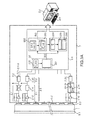
- the read circuit 2 It is shown schematically on the figure 1 the read circuit 2. It is composed, for each reading electrode 3.2, a charge preamplifier 2.10 followed by a shaping circuit 2.11.
- Several shaping circuits 2.11 can be used, it can be filters with derivations and integrations, Gaussian filters, trapezoidal filters, triangular. Often these filters are tunable and we can adjust their time constant. In general, these filters are means for forming an analog pulse whose amplitude is proportional to the charge collected by the reading electrode.
- each comparator compares the signal provided by the filter to a determined threshold and the counter increments if the threshold is exceeded. This allows a rough classification of the ionizing radiation absorbed in some energy channels. This type of circuit does not provide for parasitic signal processing.
- reading circuits furthermore comprise an analog converter in each pixel, such as the Timepix circuit developed by the Medipix collaboration or a digital-to-analog converter and a digital time converter circuit such as the ERPC circuit. the company AJAT.
- These two read circuits measure the amplitude of the pulses for each photon that has interacted in the detector. They make it possible to obtain the energy spectrum of the interactions that have occurred in each pixel of the detector. They are also able to sum the amplitude of pulses detected simultaneously in two neighboring pixels to correct the effects of charge sharing. They can not, however, distinguish pulses due to the sharing of induction and treat them as useful impulses as soon as their amplitude exceeds a threshold of detection.
- the purpose of the present invention is precisely to propose a device for detecting an ionizing radiation that corrects the effects of the induction sharing. and possibly the sharing of charges.
- the device obtained makes it possible to obtain a better spectrometric response, that is to say a more reliable estimate, than in the prior art, of the energy of the interactions, by eliminating the noise generated by the sharing of induction and possibly the sharing of charges.
- the present invention proposes a device for detecting an ionizing radiation comprising a detector made of semiconductor material intended to be polarized by means of electrodes, among which reading electrodes connected to a reading circuit which digitizes signals. they supply, these signals being processed to reject those which are the cause of the mediocre spectrometric response.
- the baseline corresponds to the signal level when there is no pulse.
- the first processing means may comprise analog processing means including a charge preamplifier possibly connected to a shaping circuit, these analog processing means being able to provide an analog pulse whose amplitude is proportional to the charge collected by one of the reading electrodes.
- the first processing means may comprise digital processing means able to supply a digitized pulse when a load has been collected by one of the reading electrodes, this digitized pulse being formed of a succession of discrete signals, these means being digital processing being downstream means of analog processing insofar as the analog processing means are present.
- the digital processing means may comprise a digitizer and possibly downstream of the digital formatting means.
- the second processing means are digital.
- They may furthermore comprise means for determining a time difference between two digitized pulses provided by the first processing means and issuing from two adjacent electrodes, and means for rejecting one of the digitized pulses and for storing the digitized pulses. another pulse scanned according to this time difference.
- the second processing means correct a load sharing.
- the time difference can be the difference between the maximum of one of the pulses and the maximum of the other of the pulses, this difference to be included in a predetermined acceptance window for the rejection means to reject one of the pulses. digitized pulses and retain the other.
- the rejection means can reject the digitized pulse whose maximum amplitude is the smallest and keep the digitized pulse whose maximum amplitude is the largest.
- the second processing means may further include means for correcting the digitized pulse stored with the rejected digitized pulse.
- Means for correcting the stored digitized pulse can add to the amplitude maximum of the digitized pulse retained the maximum amplitude of the digitized pulse rejected.
- the second processing means or the first processing means may further comprise amplitude discrimination means able to reject any pulse that said processing means have to process having a maximum amplitude less than a predetermined threshold. Thus the electronic noise is eliminated.
- the parameter determined by the second processing means may be a time parameter chosen from the rise time of the pulse, the time elapsed between the beginning of the pulse and a first zero crossing of the pulse.
- This value of the amplitude of the pulse after a passage through the baseline between the beginning and the end of the pulse may be the minimum Min (i) of the pulse.
- said temporal parameter may correspond to the duration during which the analog pulse has a positive amplitude.
- the supply step by the first processing means may provide an analog or digitized pulse.
- the processing by the second processing means may consist in determining a time difference between two digitized pulses provided by the first processing means and issuing from two adjacent electrodes, rejecting one of the digitized pulses and retaining the other digitized pulse in FIG. function of this time difference. This gives a charge sharing correction.
- processing by the second processing means may consist in correcting the digitized pulse preserved with the digitized pulse rejected.
- the method may additionally include an amplitude discrimination step for rejecting any pulse to be processed by the first processing means or the second processing means having a maximum amplitude below a predetermined threshold. This produces an elimination of the electronic noise.
- the inventors have determined three types of interfering signals which degrade the performance of the ionizing radiation detection device.
- the induced charges appear at a reading electrode 3.1, 3.2 due to the migration of charge carriers created by interaction between the ionizing radiation 5 and the semiconductor material of the detector 1.
- the pulses due to the sharing of induction obtained are not due to charges collected as a result of the interaction of the ionizing radiation 5 with the semiconductor material of the detector but to the migration, to the movement of the charge carriers in the polarized semiconductor material following the interaction.
- curve C1 represents, as a function of time, the amplitude of a pulse supplied by a charge preamplifier connected to a first reading electrode, due to the collection of charges generated by an interaction in the semiconductor material.
- This pulse is, at the beginning, of strong amplitude, it has a rather fast rise time then it decreases slowly.
- the curve C2 represents, again as a function of time, the amplitude of the pulse supplied by a charge preamplifier connected to a reading electrode close to the first reading electrode.
- the pulse is generated by induction sharing, the latter being generated by the migration of charge carriers in the vicinity of this electrode.
- the pulse has a much lower amplitude, it has a rise time and a fast descent time.
- the pulse provided by the filtering means of the read circuit is shown which, in the example, is a delay line filter.
- the amplitude of the unipolar pulse is proportional to the charge released in the semiconductor material of the detector by the interaction.
- a positive component also called positive lobe
- a negative component also called negative lobe
- the sum of the signals supplied by the reading electrodes close to a first reading electrode corresponds in principle to the charge generated during an interaction in the volume of semiconductor material associated with this first reading electrode.
- the semiconductor detector 1 provided with its electrodes 3.1, 3.2 on two main faces, preferably opposite, is substantially identical to that of the figure 1 . It is assumed that the reading electrodes 3.2 are anodes.
- the detection device also comprises a reading circuit 2 connected to each of the reading electrodes 3.2.
- This reading circuit 2 comprises, connected to each of the reading electrodes 3.2, first processing means 2.3 able to provide a pulse when a load has been collected by one of the reading electrodes 3.2.
- These first processing means 2.3 comprise in the example of the figure 3A analog processing means 2.1 including a charge pre-amplifier 2.10 connected to each of the reading electrodes 3.2 and an analog shaping circuit 2.11 connected at the output of each charge pre-amplifier 2.10.
- a 2.10 preamplifier is a means well known to those skilled in the art and it is not not described in more detail.
- the analog shaping circuit 2.11 may be a delay line filter or the like.
- the shaping circuit 2.11 is, in this example, a delay line filter. It comprises in a first branch, a delay line 21 connected to the charge preamplifier 2.10 on one side, and on the other, to a gain amplifier one 22.
- the output of the gain amplifier a 22 is connected to a negative input of a subtracter 23, this subtractor 23 having a positive input connected to the output of the charge pre-amplifier 2.10. Therefore, a signal supplied by the charge pre-amplifier 2.10 is subtracted from the same signal but delayed by the delay line 21.
- the output of the subtractor 23 supplies a gain amplifier greater than a 24.
- the output of the gain amplifier greater than one 24 provides an analog pulse whose amplitude is proportional to the charge collected by the reading electrode to which are connected the first processing means 2.3. This collected charge is generally proportional to the energy released by the ionizing radiation having interacted with the volume of semiconductor material.
- the shaping circuit 2.11 makes it possible to obtain a unipolar and generally symmetrical pulse.
- This pulse can for example be in the form of a Gaussian.
- analog processing means 2.1 could comprise only the charge pre-amplifier 2.10 and not the formatting circuit 2.11.
- the first processing means 2.3 further comprise, downstream of the analog processing means 2.1, digital processing means 2.2 comprising a digitizer 2.20 of the analog pulse supplied by the analog processing means 2.1.
- This digitizer 2.20 is formed by as many analog-digital converters as shaping circuits 2.11. Each of the analog-to-digital converters is connected to the output of a shaping circuit 2.11.
- This digitizer 2.20 converts the analog pulse supplied by the analog processing means 2.1, in the example by the shaping circuit 2.11 into a digitized pulse.
- the digitized pulse is formed of a plurality of discrete digital signals succeeding one another, they are represented by points on the Figures 4A, 4B as we will see later.
- the digitized pulse from a reading electrode i and a neighboring reading electrode i + 1 is represented during an interaction of the ionizing radiation in a volume of semiconductor material associated with the reading i.
- the denominations i and i + 1 correspond to the rank of the reading electrode on a line of successive reading electrodes.
- the digitized pulse from the electrode i reading is positive, which means that the analog processing means 2.1 also provide a positive analog pulse. But the invention naturally also applies to the case where the pulse corresponding to a measured load is negative.
- the reading circuit 2 further comprises second processing means 2.4 pulses provided by the first processing means 2.3, designed to reject any pulse that would translate an induction share.
- the second processing means 2.4 are digital, they are downstream of the digital processing means 2.2.
- the second processing means 2.4 may be formed of a microprocessor, for example, a programmable logic circuit such as an FPGA (acronym for field-programmable gate array, or network of programmable gates).
- the outputs of all the analog-to-digital converters 2.20 are connected to the input of the microprocessor 2.4.
- the second processing means 2.4 have their output connected to means 2.5 for operating the digitized pulses which have not been rejected by the second processing means 2.4, these digitized pulses are described as "conserved".
- Such operating means 2.5 comprise, for example, a microprocessor, for example that of a user device DU, such as a personal computer.
- These operating means 2.5 may comprise a spectrometry chain allowing to obtain an energy spectrum of digitized pulses that are not rejected (or conserved). They can also be made by an imager, each pixel of which represents the number of digitized pulses stored in one or more energy bands, these digitized pulses being generated by a determined anode.
- the second processing means 2.4 will perform processing on the pulses from the first processing means 2.3, so as to reject pulses that would not be useful signals, but spurious signals created by the sharing of induction and possibly the sharing loads and / or electronic noise.
- the spectrometric response of the ionizing radiation detecting device is improved.
- the digital processing means 2.20 may comprise, downstream of the digitizer 2.20, a setting circuit in form 2.110 which would then be numeric. It is outlined in dotted lines on one of the tracks of the figure 3A and the analog shaping circuit is shown barred.
- the shaping circuit 2.110 would process a digitized pulse, that is to say made of discrete digital signals.
- the formatting circuit 2.110 may comprise a line to delay, an amplifier and a subtractor arranged as previously described for the analog shaping means 2.11. Its operation is similar to that described above, except that the processed pulses are digital and more analog.
- the analog processing means 2.1 only include the charge preamplifier 2.10.
- the reading circuit 2 comprises, in the example described in FIG. figure 3A downstream of the electrodes 3.2, first processing means 2.3 intended to provide a pulse when a charge has been collected by one of the reading electrodes, these first processing means 2.3 comprising analog processing means 2.1 intended to deliver a pulse analogous when the load has been collected, this analog pulse having an amplitude proportional to the charge collected by the reading electrode and following digital processing means 2.2 of said analog pulse, including a digitizer 2.20 which delivers a digitized pulse; second processing means 2.4 of the pulse delivered by the first processing means 2.3 to reject it if it is suspected to correspond to an induction sharing and possibly a charge sharing or electronic noise.
- a digitized pulse from a first reading electrode i This digitized pulse is formed of a succession, in time, of discrete digital signals. This digitized pulse has the largest amplitude. This maximum amplitude corresponds to the maximum value of the discrete digital signals constituting it.
- this digitized pulse is unipolar, it does not cross the baseline which corresponds here to the value zero.
- the reading electrodes can be arranged in a bar or in a matrix.
- the electrodes adjacent to an electrode i will be the reading electrode which precedes i-1 and the electrode which follows i + 1.
- an electrode i is placed between an electrode i-1 and an electrode i + 1 of the same line as it. It is close to the successive electrodes h-1, h and h + 1 which are in the line preceding the line in which the electrode i is located. It is also close to the successive electrodes j-1, j and j + 1 which are in the line which follows the line in which the electrode i is located.
- the electrodes h-1, i-1, j-1 are in the same column, the electrodes h, i, j are in the same column, the electrodes h + 1, i + 1, j + 1 are in the same column .
- the second processing means 2.4 are digital and are capable of rejecting a digitized pulse corresponding to electronic noise.
- the second digital processing means 2.4 comprise means for discriminating in amplitude the discrete digital signals of a digitized pulse delivered by the first processing means 2.3.
- These discrimination means 20 comprise means 200 for determining an electronic noise discrimination threshold S_max i for the discrete digital signals of a digitized pulse. They also include means 201 for rejecting any digitized pulse of which no discrete digital signal would exceed the threshold of discrimination of the electronic noise S_max i and conservation in the opposite case.
- the threshold S_max i of electronic noise discrimination is represented and it can be seen that the digitized pulse C3 exceeds the threshold S_max i of discrimination of the electronic noise at least locally. The digitized pulse C3 will be retained.
- the threshold S_max i of electronic noise discrimination may be different from one reading electrode to another in order to take into account gain and noise dispersions related to the detector and to the electronics that follow the detector.
- the amplitude discrimination means 20 may belong to the first processing means 2.3 and be placed upstream of the digital processing means 2.20 if the first processing means 2.3 comprise digital processing means 2.20 or simply downstream from the means Analog processing 2.1. We sketched on the figure 3B said analog discriminating means 20.
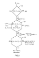
- the figure 5 diagrammatically shows an algorithm for processing the digitized pulses S (i) implemented by the read circuit and more particularly by the second processing means 2.4 which in the example are digital.
- the first block referenced 60 corresponds to an elimination step of the electronic noise.
- the second processing means 2.4 comprise means 202 for determining one or more characteristic parameters of each digitized pulse S (i) has downstream amplitude discrimination means 20.
- the determining means 202 of one or more characteristic parameters of each digitized pulse directly receive the digitized pulses of the first processing means 2.3.
- These characteristic parameters may be temporal or be a value translating an amplitude of the digitized pulse after a passage through the baseline between the beginning and the end of the digitized pulse retained.
- the temporal characteristic parameter may be, for example, the rise time ⁇ T (i) of the digitized pulse S (i) stored.
- the time parameter may be the time elapsed between the start of the digitized pulse and a first pass through the baseline of the digitized pulse.
- the value translating an amplitude of the digitized pulse after a passage through the baseline between the beginning and the end of the digitized pulse retained may be the minimum Min (i) of the digitized pulse S (i) stored, as we will explain it a little further.
- the temporal parameter can be equal to the temporal variation between two discrete digital signals constituting the digitized pulse, one of them being a discrete digital signal after passing through the baseline between the beginning and the end of the digitized pulse and the other discrete digital signal being for example the discrete digital signal illustrating the beginning of the digital pulse .
- the processing algorithm illustrated in figure 5 which is only an example, only takes into account the minimum and the rise time.
- the minimum Min (i) corresponds to the minimum discrete digital signal of the digitized pulse S (i) issued from the reading electrode i. More precisely, this minimum Min (i) corresponds to the discrete digital signal of maximum amplitude after the passage through the baseline (that is to say here by zero) of the discrete digital signals constituting the digitized pulse. Indeed, as already mentioned above, in an induction sharing situation, the analog pulse describes a first lobe, positive in the example studied, then a second lobe, negative in the example studied, after a passage through zero.
- the discrete digital signals constituting the digitized pulse S (i) issuing from the analog pulse also describe a first positive lobe, then a second negative lobe after a zero crossing at the point P, as illustrated by FIG. Figure 4A .
- the minimum discrete digital signal is the discrete digital signal of higher amplitude in the negative lobe.
- the minimum Min (i) corresponds to the discrete digital signal of maximum amplitude after the zero crossing of the digitized pulse, this definition applies as well. when the first lobe of the digitized pulse is positive only when it is negative.
- the rise time ⁇ T (i) corresponds, in principle, to the time interval between the first discrete digital signal of the digitized pulse S (i) and the discrete digital signal of maximum amplitude of the digitized pulse S ( i).
- the manner of determining the rise time ⁇ T (i) is important in the efficiency of the treatment.
- the rise time ⁇ T (i) should depend as little as possible on the maximum amplitude of the digitized pulse S (i).
- An efficient way of obtaining a rise time ⁇ T (1) which is free from the maximum amplitude is to calculate a coefficient of variation, or numerical derivative, of the digitized pulse S (i) conserved coming from the electrode i, such a coefficient of variation is positive.
- the second digital processing means 2.4 are able to derive the digitized pulse S (i).
- the Figure 4B represents the derivative of the digitized pulse of the Figure 4A for the reading electrode i (curve C3 ') and for a neighboring electrode, here the electrode i + 1 (curve C4').
- the second digital processing means 2.4 also include means 203 for rejecting any digitized pulse stored which does not satisfy at least one induction sharing criterion, relating to one of the previously determined parameters.
- the digitized pulse having satisfied the induction sharing criterion would be retained.
- rejection means 203 cooperate with the determining means 202 of the characteristic parameter or parameters reflecting an induction sharing.
- An induction sharing criterion relating to the minimum Min (i) could be: Low i > S_min i with S_min i a predetermined minimum amplitude threshold.
- a digitized pulse S (i) is due to an induction sharing, and therefore that it should not be taken into account, when the minimum discrete digital signal, or more generally, when discrete digital signal, the digitized pulse S (i) exceeds a certain threshold S_min i after passing through the baseline of this pulse, the baseline here being represented by the value zero.
- the threshold S_min i By performing a thresholding of the digitized pulse s (i), the threshold S_min i being fixed below the baseline, it is possible to discriminate pulses crossing this threshold S_min i . These pulses having crossed the threshold S_min i are considered as pulses due to an induction sharing and are therefore rejected.
- the thresholding can be achieved by identifying the maximum amplitude below the baseline, previously defined by the term Min (i) and comparing this maximum amplitude with the threshold S_min i . It can also be achieved by rejecting a digitized pulse when one of the signals crosses this threshold.
- the absolute value of the amplitude of the rebound is greater than the amplitude of the positive part of the digitized pulse.
- An induction sharing criterion relating to the rise time ⁇ T (i) can be: DT i ⁇ S_ ⁇ T i
- S_ ⁇ T i is a predetermined rise time threshold. Indeed, as we can see on the Figure 4B , the rise time of the digitized pulse corresponding to an induction sharing is greater than the rise time of a digitized pulse corresponding to a collected charge.
- the induction-sharing criterion relating to the rise time makes it possible to eliminate digitized pulses which have a rise time which is too small to correspond to a useful digitized pulse.
- the digitized pulse from the reading electrode i would be retained because it satisfies the induction sharing criterion relating to the rise time, the digitized pulse from the reading electrode i + 1 would be rejected.
- the induction sharing criterion may be relative to the temporal variation, ie to the slope, between two discrete digital signals constituting the digitized pulse, for example between the beginning of the pulse and its maximum.
- the criterion is such that the slope is compared with a certain predetermined threshold, and depending on the result of the comparison, the digitized pulse may or may not be considered as generated by an induction sharing.
- the induction sharing criterion relating to the duration between two discrete digital signals of the digitized pulse is such that, when this duration is below a certain threshold, this indicates that the digital pulse can be considered as generated by an induction sharing. On the contrary, when the digitized pulse corresponds to a collected charge, this duration slowly tends to zero.
- the second digital processing means 2.4 can apply only one of the criteria or combine several of them.
- the second block 61 corresponds to one or more steps of elimination of the induction sharing.
- the second digital processing means 2.4 may also comprise means 204 for determining digitized pulses S (i), S (i + 1) originating from two neighboring reading electrodes and capable of revealing charge sharing.
- the second digital processing means 2.4 check whether the relation below is respected: t i - t ⁇ i + 1 ⁇ ⁇
- the second digital processing means 2.4 further include means 205 for rejecting one of the two digitized pulses as revealing a sharing of charges and conservation of the other. These rejection means 205 cooperate with the determination means 204 of the two digitized pulses stored from two neighboring reading electrodes.
- the digitized pulse that is retained is the one whose maximum amplitude is the largest. The other is rejected. Note that the opposite would have been possible.
- the second digital processing means 2.4 therefore apply the relation (4) to select the digitized pulse to be retained and to reject the other digitized pulse during the charge sharing process: Max i > Max ⁇ i + 1
- the digitized pulse S (i) stored is that coming from the reading electrode i.
- the digitized pulse S (i + 1) rejected is therefore that issued from the reading electrode i + 1.
- the second digital processing means 2.4 further comprise correction means 206 of the digitized pulse S (i) selected with the digitized pulse S (i + 1) rejected. More precisely, the correction means 206 of the selected digitized pulse add to the maximum amplitude of the digitized pulse selected the maximum amplitude of the digitized pulse rejected.
- This corrected digitized pulse is a useful signal that will be exploited and which is transmitted to the operating means 2.5 by the reading circuit 2.
- the third block 62 corresponds to the steps of eliminating the shared charges.
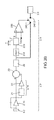
- FIG. 3B there is shown a variant of an ionizing radiation detection device according to the invention in which the first processing means 2.3 are analog and in which the second processing means 2.4 are also analog and are able to correct the sharing of 'induction.
- the first processing means do not have digital processing means.
- the first processing means 2.3 comprise, as before, a charge preamplifier 2.10 followed by a shaping means 2.11. As mentioned above, we could have only the preamplifier loads.
- the second processing means 2.4 connected at the output of the first processing means 2.3 comprise a cascade with a derivation filter 210 making it possible to obtain at the output a signal which is a derivative of the analog pulse delivered by the first processing means 2.3.
- time-amplitude converter 220 delivering a signal dependent on the duration T during which the signal delivered by the differentiating filter 210 is positive.
- the signal delivered by the time-amplitude converter 220 is applied at the input of a comparator 230, in this case in this example to the non-inverting input of the comparator 230.
- This signal delivered by the time-amplitude converter 220 is going to be compared to a predetermined set time Tmin. This set duration is applied to the other input, in this case the inverting input of the comparator 230.
- the second processing means 2.4 further comprise a switch 240 of which a first terminal 240.1 is connected at the input of the second processing means 2.4, that is to say at the output of the first processing means 2.3 and of which a second terminal 240.2 is related to the means of exploitation 2.5.
- This switch 240 is controlled by the signal delivered by the comparator 230. The control is done in such a way that the switch 240 closes when the signal delivered by the time-amplitude converter 220 has a duration T greater than the set time Tmin .
- Tmin the duration
- the control is such that the switch 240 is open and the analog pulse delivers the first means of treatment 2.3 is rejected.
- the means for determining a parameter are based on a time parameter that corresponds to the time elapsed between the beginning of the analog pulse and a first zero crossing of the analog pulse. This duration is the one during which the analog pulse has a positive amplitude.
- the second analog processing means could make it possible to determine the rise time of the analog pulse or the minimum of the analog pulse after a zero crossing of the analog pulse.
- the realization of such second analog processing means does not pose a problem to the skilled person.
- the detector is a CdTe cadmium telluride detector.
- the reading circuit 2 is in accordance with that illustrated in FIG. figure 3A .
- the source of ionizing radiation is a source of gamma radiation in cobalt 57. It emits gamma photons with an energy of about 122 keV.
- the pulses represented on the Figures 6A, 6B, 6C are delivered by a digital oscilloscope connected to the output of the analog processing means 2.1, upstream of the digital processing means 2.2, that is to say upstream of the digitizer means 2.20. It is represented by arrows, on the figure 3A where the digital oscilloscope would be connected. Unlike analogue models, in a digital oscilloscope, the signal to be visualized is digitized beforehand by an integrated analog-digital converter.
- the curves Ci-1, Ci and Ci + 1 respectively represent the analog pulses digitized by the digital oscilloscope and issued respectively from the electrodes i-1, i, i + 1.
- the curve Ci is the consequence of a gamma photon interacted with the semiconductor material associated with the reading electrode i.
- the curves Ci-1, Ci + 1 illustrate that a weak signal is induced on the neighboring pixels associated with the electrodes i-1 and i + 1.
- the curve Ci-1 is the consequence of the interaction of a gamma photon with the semiconductor material associated with the reading electrode i-1.
- the curve Ci has a significant amplitude, it corresponds to an induction sharing.
- the minimum threshold S_min i is set to a value too low, for example is equal to 0.05 V, the digitized pulse from the electrode i will be taken into account and considered as a useful signal.
- the choice of the minimum threshold S_min i is to be done with care.
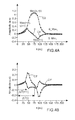
- FIGS. 7A and 7B show the energy spectrum provided by the reading circuit of an ionizing radiation detecting device produced by a cobalt gamma radiation source 57, said ionizing radiation device being provided with a cadmium telluride detector.
- this spectrum illustrates the number of shots for each channel, a channel corresponding to a division of the scale of the amplitudes of the pulses, for example a few hundred eV.
- the number of shots is the number of pulses classified in each channel.
- the spectrum shown was provided by a read circuit according to the prior art and there was no elimination of the sharing of induction, the sharing of induction corresponding to the contribution of the induced signals.
- the pulses corresponding to the induction partition have a low energy amplitude and are visible for low energy channels, the number of which is less than about 50.
- Figure 7C illustrates a case of charge sharing.
- the sum of the maximum amplitude of the curve Ci and the maximum amplitude of the curve Ci-1 corresponds substantially to the maximum amplitude of the curve Ci of the Figure 7A .
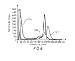
- the spectrum referenced C10 comes from digitized pulses that have not undergone any sharing correction processing. induction or charge sharing.
- the spectrum referenced C11 comes from digitized pulses having undergone the charge-sharing treatment described above and the elimination of electronic noise processing.
- the spectrum referenced C12 comes from digitized pulses having undergone, in addition to the electronic noise elimination treatment, first the treatment of the induction sharing and then the charge sharing treatment.
- the spectrum C12 is such that its peak corresponds to digitized pulses from of neighboring electrodes for which the maximum was summed, none of the two digitized pulses which were summed, has undergone an induction sharing treatment.
- the number of strokes in the peak of the C12 spectrum has been slightly increased for channels whose number is between about 120 and 170 without degrading the energy resolution too much since the charge sharing processing was performed after the sharing treatment. induction.
- energy detection threshold means the minimum detectable energy. Indeed, the signal obtained in the low energy channels is not, or is less, saturated with signals corresponding to induced signals. It represents more interactions having released a low energy.
- the fact of not using a digitized pulse affected by the induction sharing to correct a digitized pulse retained during the charge sharing process makes it possible to obtain a more reliable load sharing correction.
- the combination comprising a correction of the induced signals followed by a load sharing correction is particularly advantageous.
Landscapes
- Physics & Mathematics (AREA)
- Health & Medical Sciences (AREA)
- Life Sciences & Earth Sciences (AREA)
- General Physics & Mathematics (AREA)
- High Energy & Nuclear Physics (AREA)
- Molecular Biology (AREA)
- Spectroscopy & Molecular Physics (AREA)
- Measurement Of Radiation (AREA)
- Solid State Image Pick-Up Elements (AREA)
Applications Claiming Priority (1)
| Application Number | Priority Date | Filing Date | Title |
|---|---|---|---|
| FR1155953A FR2977328B1 (fr) | 2011-07-01 | 2011-07-01 | Dispositif de detection de rayonnement ionisant a detecteur semi-conducteur a reponse spectrometrique amelioree |
Publications (3)
| Publication Number | Publication Date |
|---|---|
| EP2541280A2 true EP2541280A2 (de) | 2013-01-02 |
| EP2541280A3 EP2541280A3 (de) | 2013-10-30 |
| EP2541280B1 EP2541280B1 (de) | 2019-01-16 |
Family
ID=46317285
Family Applications (1)
| Application Number | Title | Priority Date | Filing Date |
|---|---|---|---|
| EP12173742.3A Active EP2541280B1 (de) | 2011-07-01 | 2012-06-27 | Vorrichtung zur Erfassung von ionisierender Strahlung mit einem Halbleiterdetektor mit verbesserter spektrometrischer Ansprache |
Country Status (4)
| Country | Link |
|---|---|
| US (1) | US8748832B2 (de) |
| EP (1) | EP2541280B1 (de) |
| CN (1) | CN102854204B (de) |
| FR (1) | FR2977328B1 (de) |
Cited By (2)
| Publication number | Priority date | Publication date | Assignee | Title |
|---|---|---|---|---|
| WO2014181223A1 (en) * | 2013-05-10 | 2014-11-13 | Koninklijke Philips N.V. | Direct conversion radiation detector digital signal processing electronics |
| EP2989486A1 (de) * | 2013-04-24 | 2016-03-02 | Koninklijke Philips N.V. | Pulsverarbeitungsschaltung mit korrekturmittel |
Families Citing this family (14)
| Publication number | Priority date | Publication date | Assignee | Title |
|---|---|---|---|---|
| WO2014096746A1 (fr) * | 2012-12-21 | 2014-06-26 | Commissariat A L'energie Atomique Et Aux Energies Alternatives | Procede et dispositif de detection de rayonnement ionisant a detecteur semiconducteur |
| FR3002650B1 (fr) * | 2013-02-28 | 2015-11-27 | Commissariat Energie Atomique | Dispositif de traitement d'un signal delivre par un detecteur de rayonnement |
| JP6214031B2 (ja) * | 2013-07-19 | 2017-10-18 | 国立研究開発法人理化学研究所 | 放射線検出器のための信号データ処理方法、信号データ処理装置、および放射線検出システム |
| GB201408853D0 (en) | 2014-05-19 | 2014-07-02 | Diamond Light Source Ltd | Analysis of signals from pixellated detectors of ionizing radiation |
| US10098595B2 (en) * | 2015-08-06 | 2018-10-16 | Texas Instruments Incorporated | Low power photon counting system |
| FR3050282B1 (fr) * | 2016-04-14 | 2020-09-18 | Commissariat Energie Atomique | Dispositif de comptage de particules pour detecteur de rayonnement |
| FR3058230B1 (fr) * | 2016-10-27 | 2019-03-15 | Detection Technology Sas | Dispositif de spectrometrie |
| US10162066B2 (en) * | 2017-02-06 | 2018-12-25 | General Electric Company | Coincidence-enabling photon-counting detector |
| FR3069066B1 (fr) * | 2017-07-17 | 2019-08-16 | Commissariat A L'energie Atomique Et Aux Energies Alternatives | Procede de traitement d'une impulsion generee par un detecteur de rayonnement ionisant |
| US10151845B1 (en) | 2017-08-02 | 2018-12-11 | Texas Instruments Incorporated | Configurable analog-to-digital converter and processing for photon counting |
| US10024979B1 (en) | 2017-11-01 | 2018-07-17 | Texas Instruments Incorporated | Photon counting with coincidence detection |
| DE102017221728B4 (de) | 2017-12-01 | 2025-02-27 | Siemens Healthineers Ag | Verfahren zur Korrektur einer ortsaufgelösten Photonenmessung eines Röntgendetektors |
| WO2020142975A1 (en) * | 2019-01-10 | 2020-07-16 | Shenzhen Xpectvision Technology Co., Ltd. | Semiconductor radiation detector |
| US10890674B2 (en) | 2019-01-15 | 2021-01-12 | Texas Instruments Incorporated | Dynamic noise shaping in a photon counting system |
Family Cites Families (13)
| Publication number | Priority date | Publication date | Assignee | Title |
|---|---|---|---|---|
| US5677539A (en) * | 1995-10-13 | 1997-10-14 | Digirad | Semiconductor radiation detector with enhanced charge collection |
| FR2753278B1 (fr) | 1996-09-11 | 1998-10-09 | Commissariat Energie Atomique | Dosimetre x-gamma sensible aux basses energies |
| FR2847676B1 (fr) | 2002-11-25 | 2005-02-11 | Commissariat Energie Atomique | Cuircuit de traitement ameliore pour chaine de spectrometrie et chaine de spectrometrie utilisant un tel circuit |
| FR2868545B1 (fr) | 2004-03-31 | 2006-05-19 | Commissariat Energie Atomique | Systeme d'acquisition de spectres avec integrateur a adaptation de seuil. |
| FR2887994B1 (fr) | 2005-07-01 | 2008-05-16 | Commissariat Energie Atomique | Procede pour optimiser les performances d'un detecteur a semi-conducteur |
| FR2890750B1 (fr) | 2005-09-09 | 2007-11-02 | Commissariat Energie Atomique | Dispositif de mesure d'impulsions de courant tres breves |
| FR2907261B1 (fr) | 2006-10-12 | 2009-01-30 | Commissariat Energie Atomique | Dispositif de couplage electromagnetique d'un detecteur de rayonnement electromagnetique |
| WO2009054070A1 (ja) * | 2007-10-26 | 2009-04-30 | Shimadzu Corporation | 放射線検出器 |
| FR2925170B1 (fr) | 2007-12-13 | 2009-11-27 | Commissariat Energie Atomique | Dispositif pour realiser le traitement et la numerisation d'un spectre en energie d'un rayonnement electromagnetique |
| FR2926001A1 (fr) | 2007-12-31 | 2009-07-03 | Commissariat Energie Atomique | Dispositif de detection de rayonnements electromagnetiques a couche de transfert isotrope |
| FR2951036A1 (fr) | 2009-10-01 | 2011-04-08 | Commissariat Energie Atomique | Dispositif de traitement d'un signal delivre par un detecteur de rayonnement |
| FR2953298B1 (fr) | 2009-11-30 | 2014-10-31 | Commissariat Energie Atomique | Procede de correction du phenomene d'empilement applique a des spectres de rayonnement x acquis a l'aide d'un capteur spectrometrique |
| FR2953603A1 (fr) | 2009-12-09 | 2011-06-10 | Commissariat Energie Atomique | Procede et dispositif de reconnaissance d'un materiau a l'aide de sa fonction de transmission |
-
2011
- 2011-07-01 FR FR1155953A patent/FR2977328B1/fr not_active Expired - Fee Related
-
2012
- 2012-06-27 EP EP12173742.3A patent/EP2541280B1/de active Active
- 2012-06-28 US US13/535,852 patent/US8748832B2/en active Active
- 2012-06-29 CN CN201210222928.5A patent/CN102854204B/zh active Active
Non-Patent Citations (1)
| Title |
|---|
| None |
Cited By (4)
| Publication number | Priority date | Publication date | Assignee | Title |
|---|---|---|---|---|
| EP2989486A1 (de) * | 2013-04-24 | 2016-03-02 | Koninklijke Philips N.V. | Pulsverarbeitungsschaltung mit korrekturmittel |
| US10078009B2 (en) | 2013-04-24 | 2018-09-18 | Koninklijke Philips N.V. | Pulse processing circuit with correction means |
| WO2014181223A1 (en) * | 2013-05-10 | 2014-11-13 | Koninklijke Philips N.V. | Direct conversion radiation detector digital signal processing electronics |
| US9784854B2 (en) | 2013-05-10 | 2017-10-10 | Koninklijke Philips N.V. | Direct conversion radiation detector digital signal processing electronics |
Also Published As
| Publication number | Publication date |
|---|---|
| US8748832B2 (en) | 2014-06-10 |
| CN102854204A (zh) | 2013-01-02 |
| CN102854204B (zh) | 2017-09-08 |
| US20130168562A1 (en) | 2013-07-04 |
| EP2541280A3 (de) | 2013-10-30 |
| FR2977328B1 (fr) | 2013-08-02 |
| FR2977328A1 (fr) | 2013-01-04 |
| EP2541280B1 (de) | 2019-01-16 |
Similar Documents
| Publication | Publication Date | Title |
|---|---|---|
| EP2541280B1 (de) | Vorrichtung zur Erfassung von ionisierender Strahlung mit einem Halbleiterdetektor mit verbesserter spektrometrischer Ansprache | |
| EP2484011B1 (de) | Gerät zur verarbeitung eines signals aus einem strahlendetektor | |
| EP2510338B1 (de) | Verfahren und vorrichtung zur erkennung eines materials mittels der übertragungsfunktion | |
| EP0763751B1 (de) | Verfahren und Vorrichtung zur Korrektur von Signalen in der Gammaphotonenspektroskopie | |
| EP1704422B1 (de) | Detektionsgerät zur strahlunsmessung durch zählung von impulsen mit doppelter rücksetzschaltung | |
| WO2011067251A1 (fr) | Procédé d'étalonnage d'un détecteur de rayonnement x | |
| EP1747481B1 (de) | Messung und behandlung eines signals mit elementarimpulsbündeln | |
| EP1004040B1 (de) | Vorrichtung zur spektrometrischen messung im gebiet der detektion von gammaphotonen | |
| EP3432035B1 (de) | Verfahren und elektronisches zirkuit zur verarbeitung von von einem ionisierenden strahlungsdetektor generierten puls | |
| EP1565763B1 (de) | Verbesserte schaltungsanordnung für spektrometrie und spektrometrisches system, das diese anordnung verwendet | |
| EP1402285B1 (de) | Gerät zur verminderung der verschmierung und des dunkelstroms bei einem teilchendetektor, insbesondere bei einem photonendetektor | |
| EP3532874B1 (de) | Spektrometrievorrichtung | |
| FR2879305A1 (fr) | Traitement d'un signal representatif de rayonnement | |
| FR2945129A1 (fr) | Procede de mesure du taux de comptage d'implusions, utilisant une methode du type des temps morts reconductibles avec mesure du temps actif | |
| FR2945668A1 (fr) | Capteur d'image pour imagerie a tres bas niveau de lumiere. | |
| FR2984041A1 (fr) | Numerisation asynchrone de signaux transitoires issus de detecteurs de rayonnement | |
| WO2013014132A1 (fr) | Dispositif et procede de traitement pour une mesure spectrometrique d'un flux de photons | |
| FR3017962A1 (fr) | Outil de detection de rayonnement photonique particulierement adapte a des rayonnements a fort flux |
Legal Events
| Date | Code | Title | Description |
|---|---|---|---|
| PUAI | Public reference made under article 153(3) epc to a published international application that has entered the european phase |
Free format text: ORIGINAL CODE: 0009012 |
|
| AK | Designated contracting states |
Kind code of ref document: A2 Designated state(s): AL AT BE BG CH CY CZ DE DK EE ES FI FR GB GR HR HU IE IS IT LI LT LU LV MC MK MT NL NO PL PT RO RS SE SI SK SM TR |
|
| AX | Request for extension of the european patent |
Extension state: BA ME |
|
| PUAL | Search report despatched |
Free format text: ORIGINAL CODE: 0009013 |
|
| AK | Designated contracting states |
Kind code of ref document: A3 Designated state(s): AL AT BE BG CH CY CZ DE DK EE ES FI FR GB GR HR HU IE IS IT LI LT LU LV MC MK MT NL NO PL PT RO RS SE SI SK SM TR |
|
| AX | Request for extension of the european patent |
Extension state: BA ME |
|
| RIC1 | Information provided on ipc code assigned before grant |
Ipc: G01T 1/29 20060101AFI20130924BHEP Ipc: G01T 1/24 20060101ALI20130924BHEP |
|
| 17P | Request for examination filed |
Effective date: 20140429 |
|
| RBV | Designated contracting states (corrected) |
Designated state(s): AL AT BE BG CH CY CZ DE DK EE ES FI FR GB GR HR HU IE IS IT LI LT LU LV MC MK MT NL NO PL PT RO RS SE SI SK SM TR |
|
| STAA | Information on the status of an ep patent application or granted ep patent |
Free format text: STATUS: EXAMINATION IS IN PROGRESS |
|
| 17Q | First examination report despatched |
Effective date: 20161216 |
|
| GRAP | Despatch of communication of intention to grant a patent |
Free format text: ORIGINAL CODE: EPIDOSNIGR1 |
|
| STAA | Information on the status of an ep patent application or granted ep patent |
Free format text: STATUS: GRANT OF PATENT IS INTENDED |
|
| INTG | Intention to grant announced |
Effective date: 20180730 |
|
| GRAS | Grant fee paid |
Free format text: ORIGINAL CODE: EPIDOSNIGR3 |
|
| GRAA | (expected) grant |
Free format text: ORIGINAL CODE: 0009210 |
|
| STAA | Information on the status of an ep patent application or granted ep patent |
Free format text: STATUS: THE PATENT HAS BEEN GRANTED |
|
| AK | Designated contracting states |
Kind code of ref document: B1 Designated state(s): AL AT BE BG CH CY CZ DE DK EE ES FI FR GB GR HR HU IE IS IT LI LT LU LV MC MK MT NL NO PL PT RO RS SE SI SK SM TR |
|
| REG | Reference to a national code |
Ref country code: GB Ref legal event code: FG4D Free format text: NOT ENGLISH |
|
| REG | Reference to a national code |
Ref country code: CH Ref legal event code: EP |
|
| REG | Reference to a national code |
Ref country code: IE Ref legal event code: FG4D Free format text: LANGUAGE OF EP DOCUMENT: FRENCH |
|
| REG | Reference to a national code |
Ref country code: DE Ref legal event code: R096 Ref document number: 602012055941 Country of ref document: DE |
|
| REG | Reference to a national code |
Ref country code: AT Ref legal event code: REF Ref document number: 1090115 Country of ref document: AT Kind code of ref document: T Effective date: 20190215 |
|
| REG | Reference to a national code |
Ref country code: NL Ref legal event code: MP Effective date: 20190116 |
|
| REG | Reference to a national code |
Ref country code: LT Ref legal event code: MG4D |
|
| PG25 | Lapsed in a contracting state [announced via postgrant information from national office to epo] |
Ref country code: NL Free format text: LAPSE BECAUSE OF FAILURE TO SUBMIT A TRANSLATION OF THE DESCRIPTION OR TO PAY THE FEE WITHIN THE PRESCRIBED TIME-LIMIT Effective date: 20190116 |
|
| REG | Reference to a national code |
Ref country code: AT Ref legal event code: MK05 Ref document number: 1090115 Country of ref document: AT Kind code of ref document: T Effective date: 20190116 |
|
| PG25 | Lapsed in a contracting state [announced via postgrant information from national office to epo] |
Ref country code: FI Free format text: LAPSE BECAUSE OF FAILURE TO SUBMIT A TRANSLATION OF THE DESCRIPTION OR TO PAY THE FEE WITHIN THE PRESCRIBED TIME-LIMIT Effective date: 20190116 Ref country code: LT Free format text: LAPSE BECAUSE OF FAILURE TO SUBMIT A TRANSLATION OF THE DESCRIPTION OR TO PAY THE FEE WITHIN THE PRESCRIBED TIME-LIMIT Effective date: 20190116 Ref country code: ES Free format text: LAPSE BECAUSE OF FAILURE TO SUBMIT A TRANSLATION OF THE DESCRIPTION OR TO PAY THE FEE WITHIN THE PRESCRIBED TIME-LIMIT Effective date: 20190116 Ref country code: PL Free format text: LAPSE BECAUSE OF FAILURE TO SUBMIT A TRANSLATION OF THE DESCRIPTION OR TO PAY THE FEE WITHIN THE PRESCRIBED TIME-LIMIT Effective date: 20190116 Ref country code: PT Free format text: LAPSE BECAUSE OF FAILURE TO SUBMIT A TRANSLATION OF THE DESCRIPTION OR TO PAY THE FEE WITHIN THE PRESCRIBED TIME-LIMIT Effective date: 20190516 Ref country code: NO Free format text: LAPSE BECAUSE OF FAILURE TO SUBMIT A TRANSLATION OF THE DESCRIPTION OR TO PAY THE FEE WITHIN THE PRESCRIBED TIME-LIMIT Effective date: 20190416 Ref country code: SE Free format text: LAPSE BECAUSE OF FAILURE TO SUBMIT A TRANSLATION OF THE DESCRIPTION OR TO PAY THE FEE WITHIN THE PRESCRIBED TIME-LIMIT Effective date: 20190116 |
|
| PG25 | Lapsed in a contracting state [announced via postgrant information from national office to epo] |
Ref country code: RS Free format text: LAPSE BECAUSE OF FAILURE TO SUBMIT A TRANSLATION OF THE DESCRIPTION OR TO PAY THE FEE WITHIN THE PRESCRIBED TIME-LIMIT Effective date: 20190116 Ref country code: HR Free format text: LAPSE BECAUSE OF FAILURE TO SUBMIT A TRANSLATION OF THE DESCRIPTION OR TO PAY THE FEE WITHIN THE PRESCRIBED TIME-LIMIT Effective date: 20190116 Ref country code: GR Free format text: LAPSE BECAUSE OF FAILURE TO SUBMIT A TRANSLATION OF THE DESCRIPTION OR TO PAY THE FEE WITHIN THE PRESCRIBED TIME-LIMIT Effective date: 20190417 Ref country code: LV Free format text: LAPSE BECAUSE OF FAILURE TO SUBMIT A TRANSLATION OF THE DESCRIPTION OR TO PAY THE FEE WITHIN THE PRESCRIBED TIME-LIMIT Effective date: 20190116 Ref country code: IS Free format text: LAPSE BECAUSE OF FAILURE TO SUBMIT A TRANSLATION OF THE DESCRIPTION OR TO PAY THE FEE WITHIN THE PRESCRIBED TIME-LIMIT Effective date: 20190516 Ref country code: BG Free format text: LAPSE BECAUSE OF FAILURE TO SUBMIT A TRANSLATION OF THE DESCRIPTION OR TO PAY THE FEE WITHIN THE PRESCRIBED TIME-LIMIT Effective date: 20190416 |
|
| REG | Reference to a national code |
Ref country code: DE Ref legal event code: R097 Ref document number: 602012055941 Country of ref document: DE |
|
| PG25 | Lapsed in a contracting state [announced via postgrant information from national office to epo] |
Ref country code: EE Free format text: LAPSE BECAUSE OF FAILURE TO SUBMIT A TRANSLATION OF THE DESCRIPTION OR TO PAY THE FEE WITHIN THE PRESCRIBED TIME-LIMIT Effective date: 20190116 Ref country code: CZ Free format text: LAPSE BECAUSE OF FAILURE TO SUBMIT A TRANSLATION OF THE DESCRIPTION OR TO PAY THE FEE WITHIN THE PRESCRIBED TIME-LIMIT Effective date: 20190116 Ref country code: AL Free format text: LAPSE BECAUSE OF FAILURE TO SUBMIT A TRANSLATION OF THE DESCRIPTION OR TO PAY THE FEE WITHIN THE PRESCRIBED TIME-LIMIT Effective date: 20190116 Ref country code: RO Free format text: LAPSE BECAUSE OF FAILURE TO SUBMIT A TRANSLATION OF THE DESCRIPTION OR TO PAY THE FEE WITHIN THE PRESCRIBED TIME-LIMIT Effective date: 20190116 Ref country code: SK Free format text: LAPSE BECAUSE OF FAILURE TO SUBMIT A TRANSLATION OF THE DESCRIPTION OR TO PAY THE FEE WITHIN THE PRESCRIBED TIME-LIMIT Effective date: 20190116 Ref country code: AT Free format text: LAPSE BECAUSE OF FAILURE TO SUBMIT A TRANSLATION OF THE DESCRIPTION OR TO PAY THE FEE WITHIN THE PRESCRIBED TIME-LIMIT Effective date: 20190116 Ref country code: DK Free format text: LAPSE BECAUSE OF FAILURE TO SUBMIT A TRANSLATION OF THE DESCRIPTION OR TO PAY THE FEE WITHIN THE PRESCRIBED TIME-LIMIT Effective date: 20190116 |
|
| PLBE | No opposition filed within time limit |
Free format text: ORIGINAL CODE: 0009261 |
|
| STAA | Information on the status of an ep patent application or granted ep patent |
Free format text: STATUS: NO OPPOSITION FILED WITHIN TIME LIMIT |
|
| PG25 | Lapsed in a contracting state [announced via postgrant information from national office to epo] |
Ref country code: SM Free format text: LAPSE BECAUSE OF FAILURE TO SUBMIT A TRANSLATION OF THE DESCRIPTION OR TO PAY THE FEE WITHIN THE PRESCRIBED TIME-LIMIT Effective date: 20190116 |
|
| 26N | No opposition filed |
Effective date: 20191017 |
|
| PG25 | Lapsed in a contracting state [announced via postgrant information from national office to epo] |
Ref country code: MC Free format text: LAPSE BECAUSE OF FAILURE TO SUBMIT A TRANSLATION OF THE DESCRIPTION OR TO PAY THE FEE WITHIN THE PRESCRIBED TIME-LIMIT Effective date: 20190116 |
|
| REG | Reference to a national code |
Ref country code: CH Ref legal event code: PL |
|
| PG25 | Lapsed in a contracting state [announced via postgrant information from national office to epo] |
Ref country code: SI Free format text: LAPSE BECAUSE OF FAILURE TO SUBMIT A TRANSLATION OF THE DESCRIPTION OR TO PAY THE FEE WITHIN THE PRESCRIBED TIME-LIMIT Effective date: 20190116 |
|
| REG | Reference to a national code |
Ref country code: BE Ref legal event code: MM Effective date: 20190630 |
|
| PG25 | Lapsed in a contracting state [announced via postgrant information from national office to epo] |
Ref country code: TR Free format text: LAPSE BECAUSE OF FAILURE TO SUBMIT A TRANSLATION OF THE DESCRIPTION OR TO PAY THE FEE WITHIN THE PRESCRIBED TIME-LIMIT Effective date: 20190116 |
|
| PG25 | Lapsed in a contracting state [announced via postgrant information from national office to epo] |
Ref country code: IE Free format text: LAPSE BECAUSE OF NON-PAYMENT OF DUE FEES Effective date: 20190627 |
|
| PG25 | Lapsed in a contracting state [announced via postgrant information from national office to epo] |
Ref country code: LU Free format text: LAPSE BECAUSE OF NON-PAYMENT OF DUE FEES Effective date: 20190627 Ref country code: LI Free format text: LAPSE BECAUSE OF NON-PAYMENT OF DUE FEES Effective date: 20190630 Ref country code: BE Free format text: LAPSE BECAUSE OF NON-PAYMENT OF DUE FEES Effective date: 20190630 Ref country code: CH Free format text: LAPSE BECAUSE OF NON-PAYMENT OF DUE FEES Effective date: 20190630 |
|
| PG25 | Lapsed in a contracting state [announced via postgrant information from national office to epo] |
Ref country code: CY Free format text: LAPSE BECAUSE OF FAILURE TO SUBMIT A TRANSLATION OF THE DESCRIPTION OR TO PAY THE FEE WITHIN THE PRESCRIBED TIME-LIMIT Effective date: 20190116 |
|
| PG25 | Lapsed in a contracting state [announced via postgrant information from national office to epo] |
Ref country code: MT Free format text: LAPSE BECAUSE OF FAILURE TO SUBMIT A TRANSLATION OF THE DESCRIPTION OR TO PAY THE FEE WITHIN THE PRESCRIBED TIME-LIMIT Effective date: 20190116 Ref country code: HU Free format text: LAPSE BECAUSE OF FAILURE TO SUBMIT A TRANSLATION OF THE DESCRIPTION OR TO PAY THE FEE WITHIN THE PRESCRIBED TIME-LIMIT; INVALID AB INITIO Effective date: 20120627 |
|
| PG25 | Lapsed in a contracting state [announced via postgrant information from national office to epo] |
Ref country code: MK Free format text: LAPSE BECAUSE OF FAILURE TO SUBMIT A TRANSLATION OF THE DESCRIPTION OR TO PAY THE FEE WITHIN THE PRESCRIBED TIME-LIMIT Effective date: 20190116 |
|
| PGFP | Annual fee paid to national office [announced via postgrant information from national office to epo] |
Ref country code: DE Payment date: 20250618 Year of fee payment: 14 |
|
| PGFP | Annual fee paid to national office [announced via postgrant information from national office to epo] |
Ref country code: GB Payment date: 20250625 Year of fee payment: 14 |
|
| PGFP | Annual fee paid to national office [announced via postgrant information from national office to epo] |
Ref country code: FR Payment date: 20250623 Year of fee payment: 14 |
|
| PGFP | Annual fee paid to national office [announced via postgrant information from national office to epo] |
Ref country code: IT Payment date: 20250630 Year of fee payment: 14 |