EP2542420B1 - Dispositif d'agrandissement de moiré - Google Patents
Dispositif d'agrandissement de moiré Download PDFInfo
- Publication number
- EP2542420B1 EP2542420B1 EP11705996.4A EP11705996A EP2542420B1 EP 2542420 B1 EP2542420 B1 EP 2542420B1 EP 11705996 A EP11705996 A EP 11705996A EP 2542420 B1 EP2542420 B1 EP 2542420B1
- Authority
- EP
- European Patent Office
- Prior art keywords
- array
- microimage
- components
- colour
- image
- Prior art date
- Legal status (The legal status is an assumption and is not a legal conclusion. Google has not performed a legal analysis and makes no representation as to the accuracy of the status listed.)
- Active
Links
Images


Classifications
-
- G—PHYSICS
- G07—CHECKING-DEVICES
- G07D—HANDLING OF COINS OR VALUABLE PAPERS, e.g. TESTING, SORTING BY DENOMINATIONS, COUNTING, DISPENSING, CHANGING OR DEPOSITING
- G07D7/00—Testing specially adapted to determine the identity or genuineness of valuable papers or for segregating those which are unacceptable, e.g. banknotes that are alien to a currency
- G07D7/20—Testing patterns thereon
- G07D7/202—Testing patterns thereon using pattern matching
- G07D7/207—Matching patterns that are created by the interaction of two or more layers, e.g. moiré patterns
-
- B—PERFORMING OPERATIONS; TRANSPORTING
- B42—BOOKBINDING; ALBUMS; FILES; SPECIAL PRINTED MATTER
- B42D—BOOKS; BOOK COVERS; LOOSE LEAVES; PRINTED MATTER CHARACTERISED BY IDENTIFICATION OR SECURITY FEATURES; PRINTED MATTER OF SPECIAL FORMAT OR STYLE NOT OTHERWISE PROVIDED FOR; DEVICES FOR USE THEREWITH AND NOT OTHERWISE PROVIDED FOR; MOVABLE-STRIP WRITING OR READING APPARATUS
- B42D25/00—Information-bearing cards or sheet-like structures characterised by identification or security features; Manufacture thereof
- B42D25/30—Identification or security features, e.g. for preventing forgery
- B42D25/324—Reliefs
-
- B—PERFORMING OPERATIONS; TRANSPORTING
- B42—BOOKBINDING; ALBUMS; FILES; SPECIAL PRINTED MATTER
- B42D—BOOKS; BOOK COVERS; LOOSE LEAVES; PRINTED MATTER CHARACTERISED BY IDENTIFICATION OR SECURITY FEATURES; PRINTED MATTER OF SPECIAL FORMAT OR STYLE NOT OTHERWISE PROVIDED FOR; DEVICES FOR USE THEREWITH AND NOT OTHERWISE PROVIDED FOR; MOVABLE-STRIP WRITING OR READING APPARATUS
- B42D25/00—Information-bearing cards or sheet-like structures characterised by identification or security features; Manufacture thereof
- B42D25/30—Identification or security features, e.g. for preventing forgery
- B42D25/342—Moiré effects
-
- B—PERFORMING OPERATIONS; TRANSPORTING
- B42—BOOKBINDING; ALBUMS; FILES; SPECIAL PRINTED MATTER
- B42D—BOOKS; BOOK COVERS; LOOSE LEAVES; PRINTED MATTER CHARACTERISED BY IDENTIFICATION OR SECURITY FEATURES; PRINTED MATTER OF SPECIAL FORMAT OR STYLE NOT OTHERWISE PROVIDED FOR; DEVICES FOR USE THEREWITH AND NOT OTHERWISE PROVIDED FOR; MOVABLE-STRIP WRITING OR READING APPARATUS
- B42D25/00—Information-bearing cards or sheet-like structures characterised by identification or security features; Manufacture thereof
- B42D25/30—Identification or security features, e.g. for preventing forgery
- B42D25/351—Translucent or partly translucent parts, e.g. windows
-
- G—PHYSICS
- G07—CHECKING-DEVICES
- G07D—HANDLING OF COINS OR VALUABLE PAPERS, e.g. TESTING, SORTING BY DENOMINATIONS, COUNTING, DISPENSING, CHANGING OR DEPOSITING
- G07D7/00—Testing specially adapted to determine the identity or genuineness of valuable papers or for segregating those which are unacceptable, e.g. banknotes that are alien to a currency
- G07D7/003—Testing specially adapted to determine the identity or genuineness of valuable papers or for segregating those which are unacceptable, e.g. banknotes that are alien to a currency using security elements
-
- B42D2035/20—
-
- B42D2035/44—
-
- G—PHYSICS
- G02—OPTICS
- G02B—OPTICAL ELEMENTS, SYSTEMS OR APPARATUS
- G02B3/00—Simple or compound lenses
- G02B3/0006—Arrays
- G02B3/0037—Arrays characterized by the distribution or form of lenses
- G02B3/0056—Arrays characterized by the distribution or form of lenses arranged along two different directions in a plane, e.g. honeycomb arrangement of lenses
Definitions
- the invention relates to a moiré magnification device such as a security device, for example for use on security documents and other articles of value such as banknotes, cheques, passports, identity cards, certificates of authenticity, fiscal stamps and other documents for securing value or personal identity. It also relates to optical devices for use on packaging or the like.
- a moiré magnification device such as a security device, for example for use on security documents and other articles of value such as banknotes, cheques, passports, identity cards, certificates of authenticity, fiscal stamps and other documents for securing value or personal identity. It also relates to optical devices for use on packaging or the like.
- Moiré magnification has been used as the basis of security devices for a number of years.
- a number of examples are described in WO-A-94/27254 and EP-A-1695121 .
- a regular array of micro-focusing elements defining a focal plane is provided over a corresponding array of image elements located in a plane substantially aligned with the focal plane of the focusing elements.
- the pitch or periodicity of the array of image elements is chosen to differ by a small factor from the pitch or periodicity of the focusing elements and this mismatch means that magnified versions of the image elements are generated.
- the magnification factor depends upon the difference between the periodicities or pitches.
- a pitch mismatch between a microlens array and a microimage array can also conveniently be generated by rotating the microimage array relative to the microlens array or vice-versa, such that the microlens array and microimage array have a rotational misalignment.
- the rotational misalignment or the small pitch mismatch results in the eye observing a different part of the image in each neighbouring lens resulting in a magnified image. If the eye is then moved relative to the lens/image array a different part of the image is observed giving the impression that the image is in a different position. If the eye is moved in a smooth manner a series of images are observed giving rise to the impression that the image is moving relative to the surface.
- the nature of the movement and orientation changes can be explained from the theory of moiré; this is discussed in detail in " The theory of the Moiré phenomenon” by I. Amidror published by Kluiver Academic Publishers in 2000, ISBN 0-7923-5949-6 .
- the moiré effect of two periodic structures can be explained/predicted by considering the frequency vectors of the two structures.
- the orientation of the frequency vector represents the direction of the periodicity and the length represents the frequency (i.e. 1/Period).
- the vector is expressed by its Cartesian coordinates (u,v) where u and v are the horizontal and vertical components of the frequency.
- the focusing elements comprise microlenses or micromirrors and the image elements are defined by simple icons or the like.
- a moiré magnification device comprises a transparent substrate carrying:
- the first and second microimage components could define separate microimages and they may be spaced apart or adjacent or even abut one another.
- the two microimage components could also form parts of a larger symbol or other alphanumeric character, graphic design or the like as will be described below.
- a convenient way of achieving a variation in colour density between the microimage components is to print one in the form of a screened pattern such as a halftone screen.
- a screened pattern such as a halftone screen.
- other methods for achieving the difference in colour density could be used such as the application of different ink thicknesses.
- Different ink thicknesses can be achieved for example in gravure printing utilising a cylinder with engraved cells of varying depth or by using conventional intaglio printing.
- the first microimage components are formed by an opaque colour although this is not essential.
- the further coloured layer typically presents a uniform colour although further difficult to reproduce effects can be achieved by providing the further coloured layer in a colour which varies laterally across the device. In this way, very complex magnified versions of the microimage components can be obtained.
- the first microimage components define a first array with a first pitch and the second microimage components define a second array with a second, different pitch, each pitch being different from the pitch of the microforming elements whereby the magnified versions of the first and second components appear at different depths.
- the pitches of the two arrays differ and thus there is a risk that the microimage components of one array will overlap those of the other.
- the lateral dimensions of the first and second arrays is such that the microimage components of the first array do not overlap the microimage components of the second array.
- microimage components may typically comprise icons such as symbols, geometric figures, alphanumeric characters and the like and most preferably provide information.
- the microimage components are printed on the substrate using any suitable printing process such as gravure, wet or dry lithographic printing, screen printing, intaglio printing and flexo printing.
- the microimage components could also be formed as grating structures, recesses or other relief patterns on the substrate.
- Anti-reflection structures may also be used as described in WO-A-2005/106601 .
- Micro-focusing elements such as microlenses and concave mirrors, are preferably formed by embossing into the substrate surface, cast-curing or the like.
- Moiré magnification devices generated by the current invention can be either 2 - dimensional (2D) or 1 - dimensional (1D) structures.
- 2D moiré magnification structures using spherical lenses are described in more detail in EP-A-1695121 and WO-A-94/27254 .
- a 2D moire magnifier the microimages are magnified in all directions.
- a 1D moiré magnification structure the spherical microlenses or micromirros are replaced with a repeating arrangement of cylindrical microlenses or micromirrors. The result of this is that the micro-image elements are subject to moiré magnification in one axis only which is the axis along which the mirrors exhibit their periodic variations in curvature or relief.
- micro-images are strongly compressed or de-magnified along the magnification axis whilst the size or dimension of the micro image elements along the axis orthogonal to the magnification axis is substantially the same as they appear to the observer - i.e. no magnification or enlargement takes place.
- the moiré magnification device generated by the current invention can form a security device by itself but could also be used in conjunction with other security features such as holograms, diffraction gratings and other optically variable effect generating structures.
- the device can be used to authenticate a variety of substrates - with the nature of the substrate, in particular its thickness and flexibility having an influence on the corresponding properties of the optical device.
- the invention has particular value in protecting flexible substrates such as paper and in particular banknote, where the device could define a patch, strip or thread.
- the thickness of the device will be influenced by how its employed within the banknote though to both avoid deformation of paper ream shape during the banknote printing process and further more the form and flexibility of the banknote itself, it is desirable that the thickness of the device does not exceed half of the thickness of the banknote itself (typically 85-120um)-therefore it anticipated that in any embodiment the optical device will be less than 50um including securing adhesives and preferably substantially so.
- the desired thickness will range from a few microns (excluding securing adhesive) to a maximum of 35 - 40um (again excluding adhesive) for a label. Whilst for the case of a strip, the thickness will range again from a few micrometers for the case of a hot-stamped or transferred strip, up to 35-40um for the case of a non transferred strip wherein the supporting carrier layer is retained (again excluding securing adhesives) as would be necessary should the strip be applied over a mechanical aperture in the banknote substrate.
- final thickness is in the range of 20 -50um.
- Thicker versions of the security device could be employed in applications which include passport paper pages, plastic passport covers, visas, identity cards, brand identification labels, anti-tamper labels--any visually authenticable items.
- the device could be provided in a transparent window of a security document to enable it to be viewed in transmission.
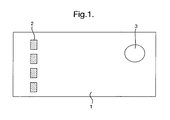
- FIG. 1 illustrates schematically a banknote 1 having a security thread 2 exposed at windows and a further transparent window 3.
- the banknote 1 may be made of paper or polymer (such as bi-axially oriented polypropylene) and one or both of the security thread 2 and window 3 incorporates a security device according to the invention.
- Figures 2-5 illustrate a comparative example of a security device.
- the appearance of the security device when viewed normally, i.e. perpendicularly is a first array 10 of magnified image elements, in this case red coloured icons 10A in the form of a figure '5' against a background 11 formed by a magnified set of blue stars in pairs of large and small stars.
- the relative depths of the icons 10A and background 11 can be seen more clearly in Figure 3 where the '5' icons 11 appear below the upper surface of the substrate 7 with the background plane 11 below the '5' icons 10A.
- Figure 4 illustrates the components of the security device in more detail.
- the background 11 is formed by an array of unit cells 11A ( Figure 4A ) arranged side by side in an array as shown in Figure 4B .
- the '5' icons 10A are formed as an array of unit cells as shown in Figures 4C and 4D .
- the pitch of the unit cells 11A of the background array 11 in the X and Y directions is A2y, A2x.
- the pitch of the '5' icons 10A is A1x, A1y.
- A2x equals A2y
- A1x equals A1y.
- Figure 5 illustrates in cross-section the overall structure of the device shown in Figures 2-4 .
- the device comprises a transparent, PET or other polymer layer 20 (corresponding to substrate 7) on the upper surface of which is formed a two-dimensional array of spherical microlenses 22.
- the diameters of the microlenses 22 is typically in the range 1-100 microns, preferably 1-50 microns and even more preferably 10-30 microns, thus defining pitches in a similar range.
- the focal length of the microlenses 22 is substantially equal to the thickness t of the optical spacer layer which in this example comprises the thickness of the substrate 20 plus the thickness of a print receptive layer 21 on the opposite surface of the substrate 20 to the microlens array 22 so as to define a focal plane 24 substantially coincident with the surface of the print receptive layer.
- the microimage array of '5' icons 10A is first printed on the print receptive layer 21 in a red colour.
- the background array 11 is printed in a blue colour. It will be seen in Figure 5 that the two arrays are each printed on the print receptive layer 21 coincident with the focal plane 24 although the background print 11 also overlaps the '5' icon array 10 as shown at 25.
- the present invention is not limited to any specific type or geometry of microlens, the only requirement being that the microlens can be used to form an image.
- Microlenses suitable for the present invention include those that refract light at a suitably curved surface of a homogenous material such as plano-convex lenslets, double convex lenslets, and fresnel lenses.
- the present invention will comprise spherical microlenses but lenses of any symmetry including cylindrical lenses could be employed. Both spherical and aspherical surfaces are applicable to the present invention. It is not essential for the microlenses to have a curved surface.
- Gradient refractive index (GRIN) lenses image light by a gradual refraction throughout the bulk of the material as a result of small variations in refractive index.
- Microlenses, based on diffraction, such as Fresnel zone plates can also be used.
- GRIN lenses and amplitude or mask based fresnel zone plates enable the surface containing the microlens array to be planar and offers advantage in print receptivity and durability.
- Master microlens arrays can be produced by number of techniques such as photothermal techniques, melt and reflow of photoresist and photoresist sculpture. Such techniques are known to those skilled in the art and are detailed in chapter 5 of " Micro-Optics: Elements, Systems, and Applications” edited by Hans Peter Herzig, published by Taylor and Francis, reprinted 1998 .
- the master microlens structure can then be physically copied by commercially available replication techniques such as hot embossing, moulding or casting.
- microlens structures can be replicated include but are not limited to thermoplastic polymers such as polycarbonate and polymethylmethacrylate (PMMA) for the hot embossing and moulding processes and acrylated epoxy materials curable by heat or radiation for the casting process.
- thermoplastic polymers such as polycarbonate and polymethylmethacrylate (PMMA) for the hot embossing and moulding processes and acrylated epoxy materials curable by heat or radiation for the casting process.
- PMMA polymethylmethacrylate
- the microlens array is replicated via casting into a UV curable coating applied to a carrier polymer film such as PET.
- a pitch mismatch is introduced between the microimage array and the microlens array.
- One method is to have a microlens and microimage array with substantially the same pitch where the pitch mismatch is achieved by introducing a small rotational misalignment between the microimage and microlens array.
- the degree of rotational misalignment between the microimage and microlens array is preferably in the range 15°- 0.05°, which results in a magnification range of between ⁇ 4X-1000X for the microimage array. More preferably the rotational misalignment is in the range 2° - 0.1°, which results in a magnification range of between ⁇ 25X-500X for the microimage array.
- microimage array and microlens array are in substantially perfect rotational alignment but with a small pitch mismatch.
- a small pitch mismatch would equate to a percentage increase/decrease of the pitch of the microimage array relative to the microlens array in the range 25% - 0.1%, which results in a magnification range of between ⁇ 4X-1000X for the microimage array.
- the percentage increase/decrease of the pitch of the microimage array relative to the microlens array is in the range 4% - 0.2%, which results in a magnification range of between ⁇ 25X-500X for the microimage array.
- the degree of magnification achieved is defined by the expressions derived in " The Moire magnifier", M. Hutley, R Hunt, R Stevens & P Savander, Pure Appl. Opt. 3 (1994) pp.133-142 .
- Figures 2a-2c show the second array 11 in different registration positions relative to the first array 10.
- the key point is that the design & choice of the first and second array elements or icons 10A, 11A is such that there is no significant change in information, content, symbolic relevance or aesthetic appearance when the position of one array is varied relative to the other - in other words the two arrays are not registration sensitive or have a strongly preferred register requirement.
- icon types which are especially information bearing, for example a denominational or alphanumeric symbol or such like are located in the first array 10 which is visualised as being in front of the second array 11.
- each unit cell 11A of the second array 11 is comprised of two identical icons i.e. a large and small star -as a consequence, in informational terms there is a redundancy of information in each unit cell.
- This redundancy property means that if at some relative registration between the two arrays the icon pattern from the first array (the 5's) substantially obscures the array of larger stars, then the smaller star icon array can be readily visualised without significant obscurement or interference from the first array.
- the describable optically variable is insensitive (i.e. substantially invariant) to uncontrolled manufacturing variations in the register of the first icon array 10 to the second array 11. This is an important aspect of this invention.
- Figures 2 & 5 were comprised of micro lenses 22 with a focal length f of 40 ⁇ m or 0.04mm. Furthermore let us suppose both the micro lenses and the supporting substrate 20 where both comprised of materials with refractive index n of 1.5. Then it follows that the base diameter D of the lenses will constrained by the expression D ⁇ f * 2 (n-1) and therefore D ⁇ 0.04 *2(1.5-1) giving D ⁇ 0.04mm.
- first image array 10 to be located 2mm behind surface plane of the substrate and the second image array 11 to be located 6mm behind the surface plane (note images behind the surface plane are by definition virtual and a more detailed analysis shows them to be non-inverted relative to micro image object array).
- the fist image array 11 In a second example suppose we required the fist image array 11 to be located 2mm in front of the surface plane, whilst the second image array 11 remains located 6mm behind the surface plane.
- the first image array 10 will form a real inverted image and thus the sign of the magnification will be negative (which follows from assigning a negative value for the image distance v in the previous expression for magnification).
- the first image array to be located in front of the surface plane (i.e appearing to float) its micro image array must have a pitch larger than the lens pitch. Conversely if the image pitch is less than the lens pitch then the image array will appear to be located below the surface plane.
- microfocussing elements comprise lenses.
- these could be replaced by concave reflectors as is known in the art.
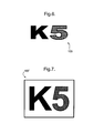
- Figure 6 shows a microimage unit cell 100 consisting in the example of a solid inked or opaque K followed by a screened (and thus semi-translucent) 5 - this screening may take the form of a linear screen as shown in Figure 6 or a half tone screen as shown in the unit cell 100' of Figure 7 or any variation in between.
- a cross-sectional view of this device is shown in Figure 8 . Illustrating a transparent plastic substrate 250 on one surface of which is provided a microlens array 252 and on the other surface a print receptive layer 251 is provided on which is provided the microimage array (layer 1) 254.
- the print receptive layer 251 can also function as a focal adjustment layer.
- the same side of the device is then over coated with a second colour 256 with the effect that the magnified synthetic image of the 5 has a colour which is the superposition of the first and second colours.
- a second colour 256 with the effect that the magnified synthetic image of the 5 has a colour which is the superposition of the first and second colours.
- the first colour used to print the K5 unit cells 100 was blue and then the second colour applied as a uniform coating 256 was yellow then it follows that in the synthetically magnified image array the K's will appear in blue (since the K was printed with a substantially opaque colour) and the 5's will appear in a shade of green, the hue of which will depend on the relative weighting of blue and yellow present in the 5's - as shown in Figure 9 .
- the background colour 256 contrasts both in hue and brightness relative to the colour of the unit cells 254.
- Ink or colorant thickness for the printed micro images is envisaged to fall in range 0.2 - 3 ⁇ m but especially 0.5 -1.0 ⁇ m.
- Ink or colorant thickness for the background colour will vary according to opacity requirements but is envisaged to fall within the range 0.5 - 5 ⁇ m and especially 1-3 ⁇ m.
- the second colour is applied as a uniform coating 256.
- the unit cell 100 comprises two separate microimage components: K and 5. It would also be possible to utilise microimage components that abut one another and form portions of a more complex image.
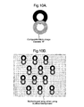
- An example is shown in Figure 10 where the unit cell in Figure 10A is made up of two microimage components, a solid circle 300 having a partial cut-out within which part of a screened circle 302 is printed.
- Figure 10B When the device is viewed ( Figure 10B ) an array of "8s" will be seen with the colour of the figure 8 varying in a vertical dimension.
- This break can conveniently be formed so as to define a cutting region when forming a security thread or the like.
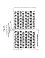
- the corresponding microimage array will look like the schematic shown in Fig 11A .
- the K and 5 have the desired mutual register - however the K array by virtue of its lesser depth and thus magnification will have a smaller pitch in both axes causing the two arrays to move out slightly out of register until at the corner location (shown top left) the two symbols are virtually touching - which we consider to be limits of acceptability.
- Fig 11A shows the center element and the top corner elements and the shift in register is characterised by the difference ⁇ X - ⁇ X 1 and the difference ⁇ Y - ⁇ Y 1 ( Fig. 11 B) .
- We may calculate the size of the array for which the shift reaches limiting value as follows: Maximum tolerated shift from center view ⁇ X - ⁇ X 1
- nx ⁇ X - ⁇ X 1 / A 1 ⁇ X - A 2 ⁇ X
- the security device could be fabricated as a mirror-based moiré device as shown in Figure 14 .
- the spherical microlens array is replaced by a spherical or aspheric concave mirror array 300 formed on one surface of the transparent polymer substrate 310.
- the other surface is provided with the same array of microimage cells as described with reference to Figure 8 .
- this printed array 254 the same side of the device is then overcoated with a second colour 256 with the effect that the magnified synthetic image of the 5 has a colour which is a superposition of the first and second colours.
- This structure is intended for viewing only in reflection mode and thus is most relevant for application onto opaque substrates (strip & patch) or partially embedding into opaque substrates (windowed thread).
- the printed micro images must be coincident with the focal plane of the mirrors to a precision determined by the depth of focus or field of the mirror system.
- the incident light has to pass through or be transmitted by the layer of the second colour and the microimage cells of the first colour before being reflected back as collimated light by the mirror array, then it follows that at least the second colour layer and at least one of the components of the microimage element (in this case the 5) must be at least partially transluscent to enable them to appear in the intended colour. If, as in this example, one of the microimage components is opaque then this component will appear black in the final device,
- the metal coating on the mirrors will also effect the background colour and the colour of the transluscent microimage component or components.
- the metal coating can be a 'white' reflector such as Aluminium or other coloured metals such as Copper or it alloys maybe be used. Other metals such as Silver, Gold, Platinum, Chrome, Nickel, Nickel-Chrome, Palladium, Tin etc may also be used.
- the focal length of a concave mirror is equal to half its radius of curvature R and therefore can have a limiting minimum value approaching one quarter of the mirror base diameter.
- the focal length and F number of a mirror can be one quarter of the value of equivalent lens (assuming typical refractive index of 1.5).
- reducing F number equates to reducing depth of focus, then in practice it will often be desirable to have a mirror base diameter much less than 2R.
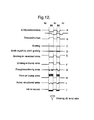
- microimage elements have been provided by printing onto the substrate. It would also be possible to provide some or all of the image elements as relief structures and examples of some of these are shown in Figures 12A-12J . In these Figures, 'IM' indicates the parts of the relief generating an image while 'NI' indicates those parts which do not generate an image.
- Figure 12A illustrates embossed or recessed image elements.
- Figure 12B illustrates debossed image elements.
- Figure 12C illustrates image elements in the form of grating structures while Figure 12D illustrates moth-eye or other fine pitch grating structures.
- Figure 12E illustrates image elements formed by gratings in recesses areas while Figure 12F illustrates gratings on debossed areas.
- Figure 12G illustrates the use of a rough embossing.
- Figure 12H illustrates the provision of print on an embossed area while Figure 12I illustrates "Aztec" shaped structures.
- Figure 12J illustrates ink filled recesses.
- the various embodiments of the device construction described above can be slit or cut into patches, foils, stripes, strips or threads for incorporation into plastic or paper substrates in accordance with known methods.
- the current invention could be incorporated into a security paper as a windowed thread.
- the security device also includes one or more other optical security features.
- a moiré magnifier device 400 is formed as described with reference to Figures 6-10 .
- the security device also includes a number of holographic image generating structures 411-416.
- the holographic image structures can be cast or embossed into the same resin as the microlenses but equally two different resins, one suitable for casting the microlenses and one suitable for embossing a holographic structure could be applied in register.
- the holographic structures could be embossed into a polymeric lacquer positioned on the opposite side of the polymeric layer to the microlenses.
- the holographic generating structures can be in the form of holograms or DOVID image elements.
- the microlenses and the magnified image array is located in a central horizontal band or region of the label whilst the holographic generating structures are located on either side.
- the holographic generating structures could be located in a central band or strip with the moiré magnifier being provided in one or more regions on either side.
- moiré magnified images and the image provided by the holographic generating structures could be integrated into a single image by each providing components of a single image.
- Figure 14 illustrates an example of such an integrated design where the holographic generating structures 420 form a scroll and in the middle of the scroll the holographic structures are replaced with a moiré magnifier 422 to create a moiré magnified image in this case of moving "5"'s and stars.
- the holographic structures can have any conventional form and can be fully or partially metallised.
- the reflection enhancing metallised layer can be replaced with a substantially transparent inorganic high refractive index layer, such as ZnS.
- the security devices shown in the previous figures are suitable to be applied as labels to secure documents which will typically require the application of a heat or pressure sensitive adhesive to the outer surface of the device which will contact the secure document.
- an optional protective coating/varnish could be applied to the exposed outer surface of the device. The function of the protective coating/varnish is to increase the durability of the device during transfer onto the security substrate and in circulation.
- the security device is preferably prefabricated on a carrier substrate and transferred to the substrate in a subsequent working step.
- the security device can be applied to the document using an adhesive layer.
- the adhesive layer is applied either to the security device or the surface of the secure document to which the device is to be applied.
- the carrier strip can be removed leaving the security device as the exposed layer or alternatively the carrier layer can remain as part of the structure acting as an outer protective layer.
- the security device of the current invention can also be incorporated as a security strip or thread.
- Security threads are now present in many of the world's currencies as well as vouchers, passports, travellers' cheques and other documents. In many cases the thread is provided in a partially embedded or windowed fashion where the thread appears to weave in and out of the paper.
- windowed threads can be found in EP0059056 .
- EP0860298 and WO03095188 describe different approaches for the embedding of wider partially exposed threads into a paper substrate. Wide threads, typically with a width of 2-6mm, are particularly useful as the additional exposed area allows for better use of optically variable devices such as the current invention.
- the security device of the current invention can be made machine readable by the introduction of detectable materials in any of the layers or by the introduction of separate machine-readable layers.
- Detectable materials that react to an external stimulus include but are not limited to fluorescent, phosphorescent, infrared absorbing, thermochromic, photochromic, magnetic, electrochromic, conductive and piezochromic materials.
- Additional optically variable materials can be included in the security device such as thin film interference elements, liquid crystal material and photonic crystal materials. Such materials may be in the form of filmic layers or as pigmented materials suitable for application by printing.
- the security device of the current invention may comprise an opaque layer.
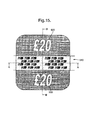
- Figures 15 and 16 show a further security feature in the form of a demetallised image 500 incorporated within a security device of the current invention.
- the moiré magnified image array 510 of the device are observed In the central band of the device.
- the structure of the feature shown in Figure 15 along section A-A is as shown in Figure 8 .
- the print receptive layer has been metallised 520.
- Parts of the metal layer are demetallised to define the demetallised images thus enabling the creation of demetallised indicia which can be viewed in reflective but more preferably transmitted light.
- the metallised layer forming the micromirrors may be extended beyond the micormirrors and then parts of this layer can be demetallised to define demetallised images.
- One way to produce partially metallised/demetallised films in which no metal is present in controlled and clearly defined areas, is to selectively demetallise regions using a resist and etch technique such as is described in US-B-4652015 .
- Other techniques for achieving similar effects are for example aluminium can be vacuum deposited through a mask, or aluminium can be selectively removed from a composite strip of a plastic carrier and aluminium using an excimer laser.
- the metallic regions may be alternatively provided by printing a metal effect ink having a metallic appearance such as Metalstar® inks sold by Eckart.
- a transparent magnetic layer can be incorporated at any position within the device structure.
- Suitable transparent magnetic layers containing a distribution of particles of a magnetic material of a size and distributed in a concentration at which the magnetic layer remains transparent are described in WO03091953 and WO03091952 .
- the security device of the current invention may be incorporated in a security document such that the device is incorporated in a transparent region of the document.
- the security document may have a substrate formed from any conventional material including paper and polymer. Techniques are known in the art for forming transparent regions in each of these types of substrate.
- WO8300659 describes a polymer banknote formed from a transparent substrate comprising an opacifying coating on both sides of the substrate. The opacifying coating is omitted in localised regions on both sides of the substrate to form a transparent region.
- EP1141480 describes a method of making a transparent region in a paper substrate. Other methods for forming transparent regions in paper substrates are described in EP0723501 , EP0724519 , EP1398174 and WO03054297 .
- One or more of the microimage arrays of the present invention may be printed with inks comprising materials that respond visibly to invisible radiation.
- Luminescent materials are known to those skilled in the art to include materials having fluorescent or phosphorescent properties. It is also well known to use other materials that respond visibly to invisible radiation such as photochromic materials and thermochromic materials.
- photochromic materials and thermochromic materials For example only one of the magnified arrays might be visible in normal daylight conditions with the second magnified image becoming visible only under UV illumination. Alternatively the two magnified arrays could appear the same colour in normal daylight conditions and different colours when viewed using a filter or when viewed under UV illumination.
Landscapes
- Engineering & Computer Science (AREA)
- Physics & Mathematics (AREA)
- General Physics & Mathematics (AREA)
- Computer Security & Cryptography (AREA)
- Computer Vision & Pattern Recognition (AREA)
- Credit Cards Or The Like (AREA)
- Printing Methods (AREA)
- Optical Elements Other Than Lenses (AREA)
- Diffracting Gratings Or Hologram Optical Elements (AREA)
- Holo Graphy (AREA)
- Stereoscopic And Panoramic Photography (AREA)
- Facsimile Scanning Arrangements (AREA)
- Color Television Image Signal Generators (AREA)
- Transforming Light Signals Into Electric Signals (AREA)
Claims (19)
- Dispositif d'agrandissement de moiré comprenant un substrat transparent supportant :i) un réseau normal d'éléments de microfocalisation sur une première surface, les éléments de focalisation définissant un plan focal ;ii) un réseau correspondant de cellules unitaires d'éléments de micro-image situé dans un plan sensiblement coïncidant avec le plan focal des éléments de focalisation, chaque cellule unitaire comprenant au moins deux composants de micro-image ;dans lequel les pas des éléments de microfocalisation et le réseau de cellules unitaires d'éléments de micro-image et leurs emplacements relatifs sont tels que le réseau d'éléments de microfocalisation coopère avec le réseau de cellules unitaires d'éléments de micro-image afin de générer des versions agrandies des composants de micro-image en raison de l'effet de moiré, caractérisé en ce que
les premiers composants de micro-image des cellules unitaires ont une densité de couleur différente de la densité de couleur des autres seconds composants de micro-image,
et dans lequel une couche colorée supplémentaire est disposée sur ou s'étendant par-dessus le réseau de cellules unitaires d'éléments de micro-image de sorte que lorsque le dispositif est visualisé, au moins les seconds composants de micro-image apparaissent dans une couleur dépendant au moins en partie de la couche colorée supplémentaire et qui est différente de la couleur des premiers composants de micro-image. - Dispositif selon la revendication 1, dans lequel les premiers et seconds composants de micro-image sont adjacents l'un à l'autre.
- Dispositif selon la revendication 2, dans lequel les premiers et seconds composants de micro-image sont contigus l'un à l'autre.
- Dispositif selon l'une quelconque des revendications précédentes, dans lequel les seconds composants de micro-image sont formés sous forme de motif tramé, de préférence une trame de demi-teinte.
- Dispositif selon l'une quelconque des revendications précédentes, dans lequel les premiers composants de micro-image sont formés par une couleur opaque.
- Dispositif selon l'une quelconque des revendications précédentes, dans lequel la couche colorée supplémentaire présente une couleur uniforme.
- Dispositif selon l'une quelconque des revendications 1 à 5, dans lequel la couleur de la couche colorée supplémentaire varie dans une direction latérale.
- Dispositif selon l'une quelconque des revendications précédentes, dans lequel les premiers composants de micro-image définissent un premier réseau avec un premier pas et les seconds composants de micro-image définissent un second réseau avec un second pas différent, chaque pas étant différent du pas des éléments de microfocalisation, de sorte que les versions agrandies des premiers et seconds composants apparaissent à différentes profondeurs, et dans lequel les dimensions latérales des premier et second réseaux sont de préférence telles que les composants de micro-image du premier réseau ne chevauchent pas les composants de micro-image du second réseau.
- Dispositif selon l'une quelconque des revendications précédentes, dans lequel les éléments de microfocalisation comprennent des microlentilles telles que des minilentilles sphériques, des minilentilles cylindriques, des minilentilles plan-convexes, des minilentilles biconvexes, des minilentilles de Fresnel et des plaques de zone de Fresnel, dans lequel chaque microlentille peut avoir un diamètre dans la plage de 1 à 100 microns, de préférence de 1 à 50 microns et de manière davantage préférée de 10 à 30 microns.
- Dispositif selon l'une quelconque des revendications 1 à 8, dans lequel les éléments de microfocalisation comprennent des miroirs concaves.
- Dispositif selon l'une quelconque des revendications précédentes, dans lequel les composants de micro-image comprennent des icônes telles que des symboles, des figures géométriques, des caractères alphanumériques, des logos et des représentations picturales.
- Dispositif selon l'une quelconque des revendications précédentes, dans lequel les composants de micro-image sont imprimés sur le substrat.
- Dispositif selon l'une quelconque des revendications 1 à 11, dans lequel les composants de micro-image sont formés sous forme de structures de grille, d'évidements ou d'autres motifs en relief sur le substrat.
- Dispositif selon l'une quelconque des revendications précédentes, dans lequel le substrat comprend un polymère tel que l'un parmi le poly(téréphtalate d'éthylène) (PET), le poly(amide), le poly(carbonate), le poly(chlorure de vinyle) (PVC), le poly(chlorure de vinylidène) (PVdC), le poly(méthacrylate de méthyle) (PMMA), le poly(naphtalate d'éthylène) (PEN) et le poly(propylène), dans lequel la distance entre le réseau d'éléments de microfocalisation et le réseau de cellules unitaires d'éléments de micro-image est de préférence dans la plage de 1 à 50 microns, de manière davantage préférée de 10 à 30 microns.
- Dispositif de sécurité selon l'une quelconque des revendications précédentes.
- Dispositif de sécurité selon la revendication 15, comprenant en outre une ou plusieurs structures de génération d'effets optiques variables situées adjacentes ou intégrées au dispositif d'agrandissement de moiré.
- Dispositif selon la revendication 15 ou la revendication 16, formé en tant que fil, étiquette ou timbre de sécurité.
- Dispositif de sécurité selon la revendication 15 ou la revendication 16, le dispositif étant disposé dans une fenêtre transparente d'un document de sécurité tel qu'un billet de banque, une carte d'identification ou similaire.
- Article pourvu d'un dispositif optique selon l'une quelconque des revendications 1 à 14, l'article comprenant l'un parmi un billet de banque, un chèque, un passeport, une carte d'identité, un certificat d'authenticité, un timbre fiscal ou un autre document de valeur de sécurité ou d'identité personnelle.
Priority Applications (1)
| Application Number | Priority Date | Filing Date | Title |
|---|---|---|---|
| PL11705996T PL2542420T3 (pl) | 2010-03-01 | 2011-03-01 | Urządzenie powiększenia mory |
Applications Claiming Priority (2)
| Application Number | Priority Date | Filing Date | Title |
|---|---|---|---|
| GBGB1003397.5A GB201003397D0 (en) | 2010-03-01 | 2010-03-01 | Moire magnification security device |
| PCT/GB2011/050407 WO2011107791A1 (fr) | 2010-03-01 | 2011-03-01 | Dispositif d'agrandissement de moiré |
Publications (3)
| Publication Number | Publication Date |
|---|---|
| EP2542420A1 EP2542420A1 (fr) | 2013-01-09 |
| EP2542420B1 true EP2542420B1 (fr) | 2014-09-24 |
| EP2542420B2 EP2542420B2 (fr) | 2022-06-01 |
Family
ID=42125795
Family Applications (5)
| Application Number | Title | Priority Date | Filing Date |
|---|---|---|---|
| EP11705995.6A Active EP2542424B2 (fr) | 2010-03-01 | 2011-03-01 | Dispositif d'agrandissement de moiré |
| EP11708074.7A Active EP2542425B2 (fr) | 2010-03-01 | 2011-03-01 | Dispositif de grossissement par effet de moiré |
| EP11705994.9A Active EP2542423B2 (fr) | 2010-03-01 | 2011-03-01 | Dispositif d'agrandissement par effet de moire |
| EP14179415.6A Active EP2811470B1 (fr) | 2010-03-01 | 2011-03-01 | Dispositif d'agrandissement de moiré |
| EP11705996.4A Active EP2542420B2 (fr) | 2010-03-01 | 2011-03-01 | Dispositif d'agrandissement de moiré |
Family Applications Before (4)
| Application Number | Title | Priority Date | Filing Date |
|---|---|---|---|
| EP11705995.6A Active EP2542424B2 (fr) | 2010-03-01 | 2011-03-01 | Dispositif d'agrandissement de moiré |
| EP11708074.7A Active EP2542425B2 (fr) | 2010-03-01 | 2011-03-01 | Dispositif de grossissement par effet de moiré |
| EP11705994.9A Active EP2542423B2 (fr) | 2010-03-01 | 2011-03-01 | Dispositif d'agrandissement par effet de moire |
| EP14179415.6A Active EP2811470B1 (fr) | 2010-03-01 | 2011-03-01 | Dispositif d'agrandissement de moiré |
Country Status (11)
| Country | Link |
|---|---|
| US (4) | US10127755B2 (fr) |
| EP (5) | EP2542424B2 (fr) |
| JP (4) | JP6006122B2 (fr) |
| CN (4) | CN102858554B (fr) |
| AU (4) | AU2011222720C1 (fr) |
| CA (4) | CA2791147C (fr) |
| ES (3) | ES2575102T3 (fr) |
| GB (1) | GB201003397D0 (fr) |
| MX (4) | MX2012009822A (fr) |
| PL (3) | PL2542424T3 (fr) |
| WO (4) | WO2011107791A1 (fr) |
Cited By (1)
| Publication number | Priority date | Publication date | Assignee | Title |
|---|---|---|---|---|
| EP3469575A4 (fr) * | 2016-06-14 | 2020-02-26 | Rolling Optics Innovation AB | Image synthéthique et procédé de fabrication associé |
Families Citing this family (134)
| Publication number | Priority date | Publication date | Assignee | Title |
|---|---|---|---|---|
| GB201003398D0 (en) * | 2010-03-01 | 2010-04-14 | Rue De Int Ltd | Optical device |
| GB201003397D0 (en) | 2010-03-01 | 2010-04-14 | Rue De Int Ltd | Moire magnification security device |
| IN2014CN02023A (fr) | 2011-08-19 | 2015-05-29 | Visual Physics Llc | |
| DE102011112554A1 (de) * | 2011-09-06 | 2013-03-07 | Giesecke & Devrient Gmbh | Verfahren zur Herstellung eines Sicherheitspapiers und Mikrolinsenfaden |
| AU2011101209B4 (en) * | 2011-09-20 | 2012-01-12 | Innovia Security Pty Ltd | A security element and method of producing a security element |
| GB201117530D0 (en) | 2011-10-11 | 2011-11-23 | Rue De Int Ltd | Security devices |
| GB201117523D0 (en) | 2011-10-11 | 2011-11-23 | Rue De Int Ltd | Security devices and methods of manufacture thereof |
| JP2013120354A (ja) * | 2011-12-08 | 2013-06-17 | Dainippon Printing Co Ltd | セキュリティ媒体及びそれを用いた真贋判定方法 |
| DE102012204343A1 (de) * | 2012-03-19 | 2013-09-19 | Bundesdruckerei Gmbh | Verfahren zur Herstellung eines Sicherheitsverbundkörpers und Sicherheitsverbundkörper mit zwei optisch brechenden Strukturen |
| GB201208137D0 (en) * | 2012-05-10 | 2012-06-20 | Rue De Int Ltd | Security devices and methods of manufacture therefor |
| CN102975568B (zh) * | 2012-05-30 | 2014-12-03 | 中钞特种防伪科技有限公司 | 光学防伪元件、使用该光学防伪元件的产品及其制备方法 |
| BR112015003455A2 (pt) | 2012-08-17 | 2017-07-04 | Visual Physics Llc | processo para transferir microestruturas para um substrato final |
| JP6061192B2 (ja) * | 2013-02-12 | 2017-01-18 | 独立行政法人 国立印刷局 | 立体表示形成体及びその作製方法 |
| EP2767395A1 (fr) * | 2013-02-15 | 2014-08-20 | KBA-NotaSys SA | Substrat pour papiers de sécurité et son procédé de fabrication |
| US20140265301A1 (en) * | 2013-03-15 | 2014-09-18 | 3M Innovative Properties Company | Security feature utlizing hinge material and biodata page |
| ES2728508T3 (es) | 2013-03-15 | 2019-10-25 | Visual Physics Llc | Dispositivo de seguridad óptico |
| US9243169B2 (en) * | 2013-05-16 | 2016-01-26 | Sicpa Holding Sa | Security laminate |
| GB2514338B (en) | 2013-05-17 | 2020-06-10 | De La Rue Int Ltd | Security documents and methods of manufacture |
| CN103278870B (zh) * | 2013-05-23 | 2015-12-02 | 苏州平流层信息科技有限公司 | 利用菲涅尔透镜制作logo的方法 |
| CN105492220A (zh) * | 2013-06-11 | 2016-04-13 | 艾利丹尼森公司 | 合成图像热转印 |
| US9873281B2 (en) | 2013-06-13 | 2018-01-23 | Visual Physics, Llc | Single layer image projection film |
| US20140367957A1 (en) * | 2013-06-13 | 2014-12-18 | Ad Lucem Corp. | Moiré magnification systems |
| CN103342060B (zh) * | 2013-06-18 | 2016-01-20 | 坤达国际有限公司 | 一种立体图像印刷品及立体图像印刷工艺 |
| TW201522101A (zh) * | 2013-07-10 | 2015-06-16 | Sicpa Holding Sa | 唯一識別符及有關此唯一識別符之高安全裝置 |
| TW201502257A (zh) * | 2013-07-10 | 2015-01-16 | Sicpa Holding Sa | 包括可印碼與手性液晶聚合物層的標記 |
| GB201313362D0 (en) | 2013-07-26 | 2013-09-11 | Rue De Int Ltd | Security Devices and Methods of Manufacture |
| GB201313363D0 (en) | 2013-07-26 | 2013-09-11 | Rue De Int Ltd | Security devices and method of manufacture |
| EP3042238A4 (fr) * | 2013-09-04 | 2017-04-19 | Lumenco LLC | Cartographie et impression de pixels pour des réseaux de micro-lentilles pour obtenir une activation à double axe d'images |
| GB201317195D0 (en) | 2013-09-27 | 2013-11-13 | Rue De Int Ltd | Method of manufacturing a pattern and apparatus therefor |
| US10019626B2 (en) * | 2013-12-02 | 2018-07-10 | Leonhard Kurz Stiftung & Co. Kg | Method for authenticating a security element, and optically variable security element |
| JP6534679B2 (ja) * | 2013-12-03 | 2019-06-26 | クレイン アンド カンパニー、 インコーポレイテッド | 1つ又は複数の向上した透かしを有するセキュリティシート又はセキュリティ文書 |
| WO2015119675A1 (fr) * | 2014-02-10 | 2015-08-13 | Uni-Pixel Displays, Inc. | Alignement optique d'un système d'impression flexographique à stations multiples à l'aide d'une interférence de moiré |
| EP2908341B1 (fr) * | 2014-02-18 | 2018-07-11 | ams AG | Dispositif semi-conducteur avec élément de focalisation intégré de surface |
| JP2017522602A (ja) | 2014-03-27 | 2017-08-10 | ビジュアル フィジクス エルエルシー | フリッカー状の光学効果を生成する光学デバイス |
| US10766292B2 (en) * | 2014-03-27 | 2020-09-08 | Crane & Co., Inc. | Optical device that provides flicker-like optical effects |
| CN106715141B (zh) | 2014-07-17 | 2020-03-17 | 光学物理有限责任公司 | 用于制造聚合物安全文件例如银行票据的改善的聚合物片材 |
| US20160133168A1 (en) * | 2014-11-06 | 2016-05-12 | Sung Jae Cho | Three-dimentional label having moving patterns using fine patterns and microlens |
| CA2961411C (fr) | 2014-09-16 | 2024-04-16 | Crane Security Technologies, Inc. | Couche de lentilles securisee |
| CN105620066B (zh) * | 2014-11-05 | 2018-03-20 | 中国科学院苏州纳米技术与纳米仿生研究所 | 透明微结构的制造方法 |
| US9971165B2 (en) * | 2014-12-30 | 2018-05-15 | Shenzhen China Star Optoelectronics Technology Co., Ltd. | 3D display apparatus |
| KR101721557B1 (ko) * | 2015-02-05 | 2017-03-30 | 손서경 | 위조방지를 위한 모아레 간섭무늬의 생성구조 |
| WO2016130822A1 (fr) | 2015-02-11 | 2016-08-18 | Crane & Co., Inc. | Procédé d'application en surface d'un dispositif de sécurité à un substrat |
| CN104614790B (zh) * | 2015-03-03 | 2016-06-22 | 苏州苏大维格光电科技股份有限公司 | 平面菲涅尔透镜阵列动态放大光学膜 |
| US10453230B2 (en) * | 2015-03-17 | 2019-10-22 | Agfa Nv | Security pattern generation method |
| GB2536877B (en) | 2015-03-23 | 2017-06-28 | De La Rue Int Ltd | Security device and method of manufacture |
| AU2015100385B4 (en) * | 2015-03-26 | 2015-07-02 | Ccl Secure Pty Ltd | An aperiodic moiré security element and method for production thereof |
| RU2017134968A (ru) * | 2015-03-26 | 2019-04-05 | СиСиЭл СИКЬЮР ПТИ ЛТД | Апериодический муаровый элемент защиты и способ его производства |
| WO2016197145A1 (fr) * | 2015-06-04 | 2016-12-08 | Chou Stephen Y | Lentille structurée à sous-longueur d'onde, utilisation et procédés de fabrication de cette dernière |
| GB2539390B (en) | 2015-06-10 | 2018-07-25 | De La Rue Int Ltd | Security devices and methods of manufacture thereof |
| DE102015008655A1 (de) * | 2015-07-03 | 2017-01-05 | Giesecke & Devrient Gmbh | Sicherheitselement mit farbfilterndem Gitter |
| GB201512118D0 (en) * | 2015-07-10 | 2015-08-19 | Rue De Int Ltd | Methods of manufacturing security documents and security devices |
| RU2728248C2 (ru) | 2015-08-27 | 2020-07-28 | Кране Секьюрити Технолоджис, Инк. | Способ одинарного или двойного перевода для подготовки и переноса четко очерченных одиночных элементов на защищаемые объекты |
| DE102015218829B4 (de) * | 2015-09-30 | 2018-08-16 | Bayerische Motoren Werke Aktiengesellschaft | Bilderzeugungsvorrichtung und Verfahren zur Herstellung eines Arrays bildgebender Elemente |
| JP6676917B2 (ja) * | 2015-10-07 | 2020-04-08 | 凸版印刷株式会社 | 表示体、および、表示体の真贋判定方法 |
| US10377162B2 (en) | 2015-10-19 | 2019-08-13 | Hydra Management Llc | Instant ticket redundancy via multi-chromatic indicia |
| CN108472979B (zh) * | 2015-10-19 | 2021-03-05 | 海德拉格莱菲克斯有限责任公司 | 打印容错的安全增强文档的方法 |
| GB201520085D0 (en) | 2015-11-13 | 2015-12-30 | Rue De Int Ltd | Methods of manufacturing image element arrays for security devices |
| CN105479974B (zh) * | 2015-12-01 | 2018-07-13 | 中钞特种防伪科技有限公司 | 一种光学防伪元件及使用该光学防伪元件的光学防伪产品 |
| US10189294B2 (en) * | 2015-12-03 | 2019-01-29 | Lumenco, Llc | Arrays of individually oriented micro mirrors for use in imaging security devices for currency and brand authentication |
| DE102015015991A1 (de) * | 2015-12-10 | 2017-06-14 | Giesecke & Devrient Gmbh | Sicherheitselement mit Linsenrasterbild |
| AU2015417708B2 (en) * | 2015-12-18 | 2021-09-23 | Visual Physics, Llc | Single layer image projection film |
| USD778941S1 (en) | 2016-01-08 | 2017-02-14 | Apple Inc. | Display screen or portion thereof with graphical user interface |
| GB2549724B (en) | 2016-04-26 | 2019-12-11 | De La Rue Int Ltd | Security devices and methods of manufacturing image patterns for security devices |
| GB2550168B (en) | 2016-05-11 | 2018-07-25 | De La Rue Int Ltd | Security device and method of manufacture |
| JP6855688B2 (ja) * | 2016-05-19 | 2021-04-07 | 株式会社村田製作所 | グラビア印刷版、グラビア印刷方法および電子部品の製造方法 |
| JP6820539B2 (ja) * | 2016-06-14 | 2021-01-27 | 大日本印刷株式会社 | 変位可視化センサー |
| JP6749633B2 (ja) * | 2016-07-11 | 2020-09-02 | 国立大学法人大阪大学 | 分光器、波長測定装置及びスペクトル測定方法 |
| GB201612290D0 (en) * | 2016-07-15 | 2016-08-31 | La Rue Int De Ltd | Methods of manufacturing a secuirty device |
| GB2557167B (en) * | 2016-09-30 | 2020-03-04 | De La Rue Int Ltd | Security devices |
| JP6256727B2 (ja) * | 2016-12-27 | 2018-01-10 | 大日本印刷株式会社 | セキュリティ媒体が配されたカード、セキュリティ媒体が配された紙 |
| ES2922024T3 (es) | 2017-02-10 | 2022-09-06 | Crane & Co Inc | Dispositivo óptico de seguridad legible por máquina |
| CN108454265B (zh) * | 2017-02-20 | 2023-09-08 | 中钞特种防伪科技有限公司 | 防伪元件及光学防伪产品 |
| GB2562775B (en) * | 2017-05-25 | 2021-06-02 | De La Rue Int Ltd | Holographic security device and method of manufacture thereof |
| GB2562797A (en) | 2017-05-26 | 2018-11-28 | De La Rue Int Ltd | Security device and method |
| AU2018280023B2 (en) * | 2017-06-05 | 2023-01-12 | Crane & Co., Inc. | An optical device that provides flicker-like optical effects |
| CN107271140B (zh) * | 2017-06-30 | 2019-05-21 | 大连理工大学 | 一种在实验水槽指定位置处产生极端波浪的方法 |
| CN109318618B (zh) * | 2017-07-31 | 2020-11-24 | 中钞特种防伪科技有限公司 | 光学防伪元件与防伪产品 |
| CN109551956B (zh) * | 2017-09-26 | 2021-11-26 | 昇印光电(昆山)股份有限公司 | 装饰片及电子设备盖板 |
| US11298966B2 (en) | 2017-09-29 | 2022-04-12 | Sicpa Holding Sa | Thin optical security element and method of designing it |
| GB2567165B (en) * | 2017-10-04 | 2020-08-26 | De La Rue Int Ltd | Improvements in security sheets comprising security elements |
| DE102017218801B3 (de) * | 2017-10-20 | 2018-11-15 | Koenig & Bauer Ag | Verfahren zur Herstellung eines Sicherheitselementes oder Sicherheitsdokumentes |
| DE102017218802B3 (de) * | 2017-10-20 | 2018-11-15 | Koenig & Bauer Ag | Verfahren zur Herstellung eines Sicherheitselementes oder Sicherheitsdokuments |
| GB2567680B (en) | 2017-10-20 | 2022-12-21 | Pulsetech Security Ltd | Holograms |
| DE102018201871B3 (de) | 2018-02-07 | 2018-12-13 | Koenig & Bauer Ag | Anordnung aufweisend ein auf ein Substrat aufgebrachtes Druckbild und eine zumindest Teile des Druckbildes abdeckende optisch abbildende Struktur |
| WO2019076805A1 (fr) | 2017-10-20 | 2019-04-25 | Koenig & Bauer Ag | Élément de sécurité ou document de sécurité |
| JP6478076B2 (ja) * | 2017-12-05 | 2019-03-06 | 大日本印刷株式会社 | セキュリティ媒体及びそれを用いた真贋判定方法、セキュリティ媒体が配されたカード、セキュリティ媒体が配された紙 |
| FR3075095B1 (fr) | 2017-12-14 | 2020-02-28 | Oberthur Fiduciaire Sas | Ensemble constitue d'un dispositif de transparence complexe et d'au moins un reseau de micro-images, ainsi que document de securite le comportant |
| DE102017130588A1 (de) * | 2017-12-19 | 2019-06-19 | Giesecke+Devrient Currency Technology Gmbh | Wertdokument |
| EP4431306A3 (fr) | 2018-01-03 | 2024-11-27 | Visual Physics, LLC | Dispositif de sécurité micro-optique à caractéristiques de sécurité dynamique interactives |
| DE102018000343A1 (de) | 2018-01-17 | 2019-07-18 | Giesecke+Devrient Currency Technology Gmbh | Sicherheitselement mit Lumineszenz-Motivbereich |
| AU2018100225A4 (en) * | 2018-02-21 | 2018-03-22 | Ccl Secure Pty Ltd | Micro-imagery design integration |
| WO2020037002A1 (fr) * | 2018-08-13 | 2020-02-20 | Crane & Co., Inc. | Film micro-optique sans lentille |
| KR102817557B1 (ko) | 2018-09-10 | 2025-06-10 | 크레인 앤 코, 인크 | 완전 마이크로-광학 보안 문서 |
| GB2578117B (en) | 2018-10-16 | 2021-06-09 | De La Rue Int Ltd | Security devices and methods for their manufacture |
| GB2578773B (en) | 2018-11-08 | 2022-03-30 | De La Rue Int Ltd | Methods of manufacturing security device components |
| GB2580069B (en) | 2018-12-20 | 2022-06-15 | De La Rue Int Ltd | Security documents and methods of manufacture thereof |
| CN109752862B (zh) * | 2019-01-10 | 2022-03-29 | 浙江理工大学 | 一种彩色图像 |
| GB2584597B (en) | 2019-03-28 | 2023-01-18 | De La Rue Int Ltd | Security device and method of manufacture thereof |
| CN111830726B (zh) * | 2019-04-19 | 2023-03-17 | 昇印光电(昆山)股份有限公司 | 3d成像薄膜 |
| CN113795390B (zh) | 2019-05-20 | 2024-08-20 | 克瑞尼股份有限公司 | 使用纳米颗粒调谐聚合物基质层的折射率以优化微光学(mo)聚焦 |
| GB2589818B (en) | 2019-07-12 | 2022-12-14 | De La Rue Int Ltd | Security devices and methods of manufacture thereof |
| US11685180B2 (en) | 2019-08-19 | 2023-06-27 | Crane & Co., Inc. | Micro-optic security device with zones of color |
| CN112505940B (zh) * | 2019-08-26 | 2023-03-24 | 昇印光电(昆山)股份有限公司 | 一种立体成像光学薄膜 |
| CN118466040A (zh) | 2019-08-26 | 2024-08-09 | 昇印光电(昆山)股份有限公司 | 光学成像膜 |
| CN112505938B (zh) * | 2019-08-26 | 2022-07-05 | 昇印光电(昆山)股份有限公司 | 立体成像膜 |
| GB201913913D0 (en) * | 2019-09-26 | 2019-11-13 | Optrical Ltd | Improvements in and relating to security devices |
| KR102153234B1 (ko) * | 2019-09-26 | 2020-09-07 | 지제이엠 주식회사 | 입체 시트 라벨 |
| GB2588625B (en) | 2019-10-29 | 2022-12-14 | De La Rue Int Ltd | Method of forming a security device |
| CN112848742A (zh) * | 2019-11-27 | 2021-05-28 | 中钞特种防伪科技有限公司 | 光学防伪元件及光学防伪产品 |
| DE112020005501T5 (de) * | 2019-12-19 | 2022-08-25 | CCL Secure Pty Ltd. | Mikrooptische Vorrichtung |
| EP3888929B1 (fr) * | 2020-03-31 | 2022-05-11 | NWM Research Spolka z ograniczona Odpowiedzialnoscia Spolka komandytowa | Procédé de fabrication d'une microstructure de sécurité optique discrétisée sur un substrat et shim à utiliser dans le procédé |
| GB2594300A (en) * | 2020-04-22 | 2021-10-27 | De La Rue Int Ltd | Security documents and methods of manufacture thereof |
| JP7622355B2 (ja) * | 2020-05-19 | 2025-01-28 | Toppanホールディングス株式会社 | 表示体 |
| JP7468137B2 (ja) * | 2020-05-19 | 2024-04-16 | Toppanホールディングス株式会社 | 表示体 |
| CN111572235B (zh) * | 2020-05-21 | 2021-09-14 | 苏州大学 | 一种隐藏式立体成像薄膜 |
| US11577540B2 (en) | 2020-05-29 | 2023-02-14 | Capital One Services, Llc | Financial card with dynamic viewing angles to block card information |
| CN111554195B (zh) * | 2020-05-30 | 2022-06-14 | 京东方科技集团股份有限公司 | 柔性显示模组及其制备方法、电子设备 |
| CN113946002A (zh) * | 2020-07-17 | 2022-01-18 | 英属开曼群岛商音飞光电科技股份有限公司 | 摩尔纹成像装置 |
| GB2601036B (en) | 2020-09-11 | 2023-05-10 | De La Rue Int Ltd | Security devices and methods of manufacture thereof |
| JP7537211B2 (ja) * | 2020-09-29 | 2024-08-21 | Toppanホールディングス株式会社 | 表示体 |
| CA3201614A1 (fr) * | 2020-12-11 | 2022-06-16 | Axel Lundvall | Fabrication d'images synthetiques avec animation continue |
| GB2592719B (en) | 2020-12-15 | 2024-01-17 | Koenig & Bauer Banknote Solutions Sa | Methods for designing and producing a security feature |
| GB2602796B (en) | 2021-01-11 | 2023-08-23 | De La Rue Int Ltd | Optical devices and methods of manufacture thereof |
| GB202101267D0 (en) | 2021-01-29 | 2021-03-17 | De La Rue Int Ltd | Security devices and methods of manufacture thereof |
| DE102021001019A1 (de) | 2021-02-25 | 2022-08-25 | Giesecke+Devrient Currency Technology Gmbh | Sicherheitselement, Datenträger und Herstellungsverfahren |
| US20240174019A1 (en) * | 2021-03-08 | 2024-05-30 | Crane & Co., Inc. | Micro-optic security device with multi-phase icon structure |
| WO2023023453A1 (fr) * | 2021-08-16 | 2023-02-23 | Crane & Co., Inc. | Dispositif de sécurité micro-optique à résistance améliorée à la récolte marquée par l'humidité |
| CA3143656A1 (fr) * | 2021-12-22 | 2023-06-22 | Bank Of Canada | Dispositifs de securite micro-optiques dynamiques, production et utilisation |
| CN118891584A (zh) | 2022-03-10 | 2024-11-01 | 巴斯夫欧洲公司 | 用于丝网印刷的浇铸漆 |
| DE102022111098B3 (de) | 2022-05-05 | 2023-06-01 | Koenig & Bauer Ag | Druckmaschine zur Herstellung eines Sicherheitsdokuments |
| DE102022111096B3 (de) | 2022-05-05 | 2023-08-24 | Koenig & Bauer Ag | Verfahren zum Authentifizieren eines Sicherheitsdokuments |
| DE102022111099B3 (de) | 2022-05-05 | 2023-06-01 | Koenig & Bauer Ag | Sicherheitsdokument mit einem in seinem Substrat ausgebildeten transparenten Fenster |
| DE102022111097B3 (de) | 2022-05-05 | 2023-06-01 | Koenig & Bauer Ag | Sicherheitsdokument mit einem in seinem Substrat ausgebildeten transparenten Fenster |
| CN117677087B (zh) * | 2022-08-25 | 2024-10-29 | 比亚迪股份有限公司 | 光学结构、终端壳体及终端 |
Family Cites Families (62)
| Publication number | Priority date | Publication date | Assignee | Title |
|---|---|---|---|---|
| US3357773A (en) * | 1964-12-31 | 1967-12-12 | Rowland Products Inc | Patterned sheet material |
| GB1407065A (en) | 1972-11-30 | 1975-09-24 | Rue Co Ltd Thomas De | Production of security documents |
| IN157644B (fr) | 1981-02-19 | 1986-05-10 | Portals Ltd | |
| AU558476B2 (en) | 1981-08-24 | 1987-01-29 | Securency Pty Ltd | Improved bank notes and the like |
| US4652015A (en) | 1985-12-05 | 1987-03-24 | Crane Company | Security paper for currency and banknotes |
| GB2204272B (en) | 1987-02-18 | 1991-06-19 | Metal Box Plc | Security documents |
| JP2581142B2 (ja) | 1988-03-29 | 1997-02-12 | 日本鋼管株式会社 | オーステナイト系ステンレス鋼材溶接部の耐硝酸腐食性改善方法 |
| GB9211123D0 (en) * | 1992-05-26 | 1992-07-08 | Amblehurst Ltd | Holographic device |
| DE4314380B4 (de) | 1993-05-01 | 2009-08-06 | Giesecke & Devrient Gmbh | Sicherheitspapier und Verfahren zu seiner Herstellung |
| GB9309673D0 (en) | 1993-05-11 | 1993-06-23 | De La Rue Holographics Ltd | Security device |
| AU5538094A (en) | 1993-05-14 | 1994-12-12 | Worldwide Notification Systems, Inc. | Apparatus and method of notifying a recipient of an unscheduled delivery |
| AT401365B (de) | 1993-10-11 | 1996-08-26 | Oesterr Nationalbank | Wertpapier |
| DE4334847A1 (de) | 1993-10-13 | 1995-04-20 | Kurz Leonhard Fa | Wertdokument mit Fenster |
| GB2350319B (en) | 1996-06-14 | 2001-01-10 | Rue De Int Ltd | Security printed device |
| JP3338860B2 (ja) | 1996-07-17 | 2002-10-28 | ヤマックス株式会社 | 点描画模様の装飾体 |
| GB9828770D0 (en) | 1998-12-29 | 1999-02-17 | Rue De Int Ltd | Security paper |
| JP2001026175A (ja) | 1999-07-14 | 2001-01-30 | Sony Corp | 段ボールの印刷方法及び梱包用段ボール |
| BR0007172A (pt) | 1999-09-30 | 2001-09-04 | Koninkl Philips Electronics Nv | Dispositivo lenticular, e, conjunto de dispositivos lenticulares |
| US6450540B1 (en) | 2000-11-15 | 2002-09-17 | Technology Tree Co., Ltd | Printed matter displaying various colors according to view angle |
| JP2003039583A (ja) | 2001-07-27 | 2003-02-13 | Meiwa Gravure Co Ltd | 装飾シート |
| DE10163381A1 (de) | 2001-12-21 | 2003-07-03 | Giesecke & Devrient Gmbh | Sicherheitspapier sowie Verfahren und Vorrichtung zu seiner Herstellung |
| GB0209564D0 (en) | 2002-04-25 | 2002-06-05 | Rue De Int Ltd | Improvements in substrates |
| GB2388377B (en) | 2002-05-09 | 2004-07-28 | Rue De Int Ltd | A paper sheet incorporating a security element and a method of making the same |
| EP1398174A1 (fr) | 2002-09-10 | 2004-03-17 | Kba-Giori S.A. | Substrat renforcé pour papiers de valeur |
| US7194105B2 (en) | 2002-10-16 | 2007-03-20 | Hersch Roger D | Authentication of documents and articles by moiré patterns |
| US7429062B2 (en) * | 2002-10-30 | 2008-09-30 | Xerox Corporation | Anti-counterfeiting see-through moire security feature using frequency-varying patterns |
| JP2004317636A (ja) | 2003-04-14 | 2004-11-11 | Sanko Sangyo Co Ltd | 被観察体 |
| JP4337114B2 (ja) * | 2003-06-16 | 2009-09-30 | ヤマックス株式会社 | 虚像現出装飾体 |
| EP2258560A3 (fr) | 2003-11-21 | 2011-04-13 | Visual Physics, LLC | Sécurité micro-optique et système de présentation d'images |
| AU2005238699B2 (en) * | 2004-04-30 | 2008-11-20 | De La Rue International Limited | Arrays of microlenses and arrays of microimages on transparent security substrates |
| DE102004044458B4 (de) * | 2004-09-15 | 2010-01-07 | Ovd Kinegram Ag | Sicherheitsdokument |
| DE102004056553B4 (de) | 2004-11-23 | 2013-03-14 | Giesecke & Devrient Gmbh | Sicherheitsanordnung für Sicherheitsdokumente und Verfahren zum Herstellen der Sicherheitsdokumente |
| JP4590614B2 (ja) * | 2005-01-13 | 2010-12-01 | 独立行政法人 国立印刷局 | 偽造防止印刷物 |
| DE102005007749A1 (de) * | 2005-02-18 | 2006-08-31 | Giesecke & Devrient Gmbh | Sicherheitselement und Verfahren zu seiner Herstellung |
| DE102005028162A1 (de) * | 2005-02-18 | 2006-12-28 | Giesecke & Devrient Gmbh | Sicherheitselement und Verfahren zu seiner Herstellung |
| US20080284157A1 (en) * | 2005-03-29 | 2008-11-20 | Sani Muke | Tamper Evident Identification Documents |
| ES2563755T3 (es) | 2005-05-18 | 2016-03-16 | Visual Physics, Llc | Presentación de imágenes y sistema de seguridad micro-óptico |
| WO2007007793A1 (fr) | 2005-07-12 | 2007-01-18 | Grapac Japan Co., Inc. | Structure de feuille stéréoscopique |
| ES2313264T3 (es) * | 2005-09-20 | 2009-03-01 | ALCAN TECHNOLOGY & MANAGEMENT LTD. | Objeto con efecto optico. |
| DE102005062132A1 (de) | 2005-12-23 | 2007-07-05 | Giesecke & Devrient Gmbh | Sicherheitselement |
| CN101443692B (zh) * | 2006-05-12 | 2012-11-21 | 克瑞尼股份有限公司 | 微型光学膜结构、安全文件或标签及其鉴定方法 |
| DE102006029850A1 (de) | 2006-06-27 | 2008-01-03 | Giesecke & Devrient Gmbh | Sicherheitselement |
| DE102006029852A1 (de) | 2006-06-27 | 2008-01-03 | Giesecke & Devrient Gmbh | Verfahren zum Aufbringen einer Mikrostruktur, Werkzeugform und Gegenstand mit Mikrostruktur |
| KR101376434B1 (ko) | 2006-06-28 | 2014-04-01 | 비쥬얼 피직스 엘엘씨 | 마이크로-광학 보안 및 화상 표시 시스템 |
| JP2008012870A (ja) | 2006-07-07 | 2008-01-24 | Grapac Japan Kk | 立体視シート構成体 |
| US20080258457A1 (en) | 2006-09-08 | 2008-10-23 | De La Rue International Limited | Method of manufacturing a security device |
| DE102007005414A1 (de) † | 2007-01-30 | 2008-08-07 | Ovd Kinegram Ag | Sicherheitselement zur Sicherung von Wertdokumenten |
| BE1017460A6 (nl) | 2007-02-09 | 2008-10-07 | Leo Vermeulen Consulting Lvc | Lenticulair folie. |
| DE102007029203A1 (de) * | 2007-06-25 | 2009-01-08 | Giesecke & Devrient Gmbh | Sicherheitselement |
| DE102007029204A1 (de) * | 2007-06-25 | 2009-01-08 | Giesecke & Devrient Gmbh | Sicherheitselement |
| JP5233227B2 (ja) | 2007-09-28 | 2013-07-10 | 凸版印刷株式会社 | 表示体及びラベル付き物品 |
| DE102008016795A1 (de) † | 2008-04-02 | 2009-10-08 | Giesecke & Devrient Gmbh | Verfahren zum Erzeugen einer mikrooptischen Moiré-Vergrößerungsanordnung |
| JP4953026B2 (ja) | 2008-04-23 | 2012-06-13 | ヤマックス株式会社 | 装飾体 |
| JP5131789B2 (ja) * | 2008-05-01 | 2013-01-30 | 独立行政法人 国立印刷局 | 画像形成体、真偽判別具及び真偽判別方法 |
| DE102008029638A1 (de) | 2008-06-23 | 2009-12-24 | Giesecke & Devrient Gmbh | Sicherheitselement |
| AU2009278274B2 (en) † | 2008-08-05 | 2013-08-01 | Giesecke & Devrient Gmbh | Security arrangement |
| US20110233918A1 (en) | 2008-11-18 | 2011-09-29 | Rolling Optics Ab | Time integrated integral image device |
| CN101434176B (zh) * | 2008-12-25 | 2012-11-07 | 中钞特种防伪科技有限公司 | 光学防伪元件及带有该光学防伪元件的产品 |
| DE102009040975A1 (de) | 2009-09-11 | 2011-03-24 | Ovd Kinegram Ag | Mehrschichtkörper |
| FR2952194B1 (fr) | 2009-10-30 | 2012-04-20 | Arjowiggins Security | Element de securite comportant un substrat portant une structure optique et un motif de reference, et procede associe. |
| GB0919108D0 (en) * | 2009-10-30 | 2009-12-16 | Rue De Int Ltd | Security device |
| GB201003397D0 (en) | 2010-03-01 | 2010-04-14 | Rue De Int Ltd | Moire magnification security device |
-
2010
- 2010-03-01 GB GBGB1003397.5A patent/GB201003397D0/en not_active Ceased
-
2011
- 2011-03-01 WO PCT/GB2011/050407 patent/WO2011107791A1/fr not_active Ceased
- 2011-03-01 JP JP2012555489A patent/JP6006122B2/ja not_active Expired - Fee Related
- 2011-03-01 AU AU2011222720A patent/AU2011222720C1/en active Active
- 2011-03-01 CA CA2791147A patent/CA2791147C/fr not_active Expired - Fee Related
- 2011-03-01 US US13/580,784 patent/US10127755B2/en not_active Expired - Fee Related
- 2011-03-01 MX MX2012009822A patent/MX2012009822A/es active IP Right Grant
- 2011-03-01 CA CA2791160A patent/CA2791160C/fr not_active Expired - Fee Related
- 2011-03-01 JP JP2012555491A patent/JP6068145B2/ja not_active Expired - Fee Related
- 2011-03-01 AU AU2011222723A patent/AU2011222723C1/en active Active
- 2011-03-01 CN CN201180021465.XA patent/CN102858554B/zh not_active Expired - Fee Related
- 2011-03-01 CN CN201180015130.7A patent/CN102869517B/zh not_active Expired - Fee Related
- 2011-03-01 US US13/580,730 patent/US9177433B2/en not_active Expired - Fee Related
- 2011-03-01 MX MX2012010058A patent/MX2012010058A/es active IP Right Grant
- 2011-03-01 MX MX2012009918A patent/MX2012009918A/es active IP Right Grant
- 2011-03-01 ES ES14179415.6T patent/ES2575102T3/es active Active
- 2011-03-01 JP JP2012555490A patent/JP6162404B2/ja not_active Expired - Fee Related
- 2011-03-01 US US13/580,837 patent/US8908276B2/en not_active Expired - Fee Related
- 2011-03-01 EP EP11705995.6A patent/EP2542424B2/fr active Active
- 2011-03-01 WO PCT/GB2011/050398 patent/WO2011107782A1/fr not_active Ceased
- 2011-03-01 ES ES11705995.6T patent/ES2519595T3/es active Active
- 2011-03-01 EP EP11708074.7A patent/EP2542425B2/fr active Active
- 2011-03-01 PL PL11705995T patent/PL2542424T3/pl unknown
- 2011-03-01 CN CN201180022006.3A patent/CN102869518B/zh not_active Expired - Fee Related
- 2011-03-01 JP JP2012555488A patent/JP5937522B2/ja not_active Expired - Fee Related
- 2011-03-01 WO PCT/GB2011/050404 patent/WO2011107788A1/fr not_active Ceased
- 2011-03-01 ES ES11705996.4T patent/ES2519596T3/es active Active
- 2011-03-01 EP EP11705994.9A patent/EP2542423B2/fr active Active
- 2011-03-01 AU AU2011222714A patent/AU2011222714C1/en active Active
- 2011-03-01 CN CN201180011752.2A patent/CN102844198B/zh not_active Expired - Fee Related
- 2011-03-01 CA CA2791055A patent/CA2791055C/fr not_active Expired - Fee Related
- 2011-03-01 US US13/580,797 patent/US9070237B2/en not_active Expired - Fee Related
- 2011-03-01 EP EP14179415.6A patent/EP2811470B1/fr active Active
- 2011-03-01 AU AU2011222715A patent/AU2011222715C1/en active Active
- 2011-03-01 EP EP11705996.4A patent/EP2542420B2/fr active Active
- 2011-03-01 MX MX2012010057A patent/MX2012010057A/es active IP Right Grant
- 2011-03-01 CA CA2791161A patent/CA2791161C/fr not_active Expired - Fee Related
- 2011-03-01 PL PL11705996T patent/PL2542420T3/pl unknown
- 2011-03-01 WO PCT/GB2011/050399 patent/WO2011107783A1/fr not_active Ceased
- 2011-03-01 PL PL14179415.6T patent/PL2811470T3/pl unknown
Cited By (2)
| Publication number | Priority date | Publication date | Assignee | Title |
|---|---|---|---|---|
| EP3469575A4 (fr) * | 2016-06-14 | 2020-02-26 | Rolling Optics Innovation AB | Image synthéthique et procédé de fabrication associé |
| EP3469574B1 (fr) | 2016-06-14 | 2025-02-19 | Rolling Optics Innovation AB | Image synthétique et procédé de fabrication associé |
Also Published As
Similar Documents
| Publication | Publication Date | Title |
|---|---|---|
| EP2542420B1 (fr) | Dispositif d'agrandissement de moiré | |
| US20130044362A1 (en) | Optical device |
Legal Events
| Date | Code | Title | Description |
|---|---|---|---|
| PUAI | Public reference made under article 153(3) epc to a published international application that has entered the european phase |
Free format text: ORIGINAL CODE: 0009012 |
|
| 17P | Request for examination filed |
Effective date: 20120903 |
|
| AK | Designated contracting states |
Kind code of ref document: A1 Designated state(s): AL AT BE BG CH CY CZ DE DK EE ES FI FR GB GR HR HU IE IS IT LI LT LU LV MC MK MT NL NO PL PT RO RS SE SI SK SM TR |
|
| DAX | Request for extension of the european patent (deleted) | ||
| REG | Reference to a national code |
Ref country code: DE Ref legal event code: R079 Ref document number: 602011010097 Country of ref document: DE Free format text: PREVIOUS MAIN CLASS: B42D0015000000 Ipc: G02B0003000000 |
|
| RIC1 | Information provided on ipc code assigned before grant |
Ipc: G07D 7/20 20060101ALI20140130BHEP Ipc: G07D 7/00 20060101ALI20140130BHEP Ipc: G02B 3/00 20060101AFI20140130BHEP Ipc: B42D 15/00 20060101ALI20140130BHEP |
|
| GRAP | Despatch of communication of intention to grant a patent |
Free format text: ORIGINAL CODE: EPIDOSNIGR1 |
|
| INTG | Intention to grant announced |
Effective date: 20140417 |
|
| GRAS | Grant fee paid |
Free format text: ORIGINAL CODE: EPIDOSNIGR3 |
|
| GRAA | (expected) grant |
Free format text: ORIGINAL CODE: 0009210 |
|
| AK | Designated contracting states |
Kind code of ref document: B1 Designated state(s): AL AT BE BG CH CY CZ DE DK EE ES FI FR GB GR HR HU IE IS IT LI LT LU LV MC MK MT NL NO PL PT RO RS SE SI SK SM TR |
|
| REG | Reference to a national code |
Ref country code: GB Ref legal event code: FG4D |
|
| REG | Reference to a national code |
Ref country code: CH Ref legal event code: EP |
|
| REG | Reference to a national code |
Ref country code: AT Ref legal event code: REF Ref document number: 688859 Country of ref document: AT Kind code of ref document: T Effective date: 20141015 |
|
| REG | Reference to a national code |
Ref country code: IE Ref legal event code: FG4D |
|
| REG | Reference to a national code |
Ref country code: NL Ref legal event code: T3 |
|
| REG | Reference to a national code |
Ref country code: DE Ref legal event code: R096 Ref document number: 602011010097 Country of ref document: DE Effective date: 20141106 |
|
| REG | Reference to a national code |
Ref country code: ES Ref legal event code: FG2A Ref document number: 2519596 Country of ref document: ES Kind code of ref document: T3 Effective date: 20141107 |
|
| REG | Reference to a national code |
Ref country code: SE Ref legal event code: TRGR |
|
| REG | Reference to a national code |
Ref country code: PL Ref legal event code: T3 |
|
| PG25 | Lapsed in a contracting state [announced via postgrant information from national office to epo] |
Ref country code: NO Free format text: LAPSE BECAUSE OF FAILURE TO SUBMIT A TRANSLATION OF THE DESCRIPTION OR TO PAY THE FEE WITHIN THE PRESCRIBED TIME-LIMIT Effective date: 20141224 Ref country code: FI Free format text: LAPSE BECAUSE OF FAILURE TO SUBMIT A TRANSLATION OF THE DESCRIPTION OR TO PAY THE FEE WITHIN THE PRESCRIBED TIME-LIMIT Effective date: 20140924 Ref country code: LT Free format text: LAPSE BECAUSE OF FAILURE TO SUBMIT A TRANSLATION OF THE DESCRIPTION OR TO PAY THE FEE WITHIN THE PRESCRIBED TIME-LIMIT Effective date: 20140924 Ref country code: GR Free format text: LAPSE BECAUSE OF FAILURE TO SUBMIT A TRANSLATION OF THE DESCRIPTION OR TO PAY THE FEE WITHIN THE PRESCRIBED TIME-LIMIT Effective date: 20141225 |
|
| REG | Reference to a national code |
Ref country code: LT Ref legal event code: MG4D |
|
| PG25 | Lapsed in a contracting state [announced via postgrant information from national office to epo] |
Ref country code: HR Free format text: LAPSE BECAUSE OF FAILURE TO SUBMIT A TRANSLATION OF THE DESCRIPTION OR TO PAY THE FEE WITHIN THE PRESCRIBED TIME-LIMIT Effective date: 20140924 Ref country code: RS Free format text: LAPSE BECAUSE OF FAILURE TO SUBMIT A TRANSLATION OF THE DESCRIPTION OR TO PAY THE FEE WITHIN THE PRESCRIBED TIME-LIMIT Effective date: 20140924 Ref country code: LV Free format text: LAPSE BECAUSE OF FAILURE TO SUBMIT A TRANSLATION OF THE DESCRIPTION OR TO PAY THE FEE WITHIN THE PRESCRIBED TIME-LIMIT Effective date: 20140924 Ref country code: CY Free format text: LAPSE BECAUSE OF FAILURE TO SUBMIT A TRANSLATION OF THE DESCRIPTION OR TO PAY THE FEE WITHIN THE PRESCRIBED TIME-LIMIT Effective date: 20140924 |
|
| REG | Reference to a national code |
Ref country code: FR Ref legal event code: PLFP Year of fee payment: 5 |
|
| PG25 | Lapsed in a contracting state [announced via postgrant information from national office to epo] |
Ref country code: PT Free format text: LAPSE BECAUSE OF FAILURE TO SUBMIT A TRANSLATION OF THE DESCRIPTION OR TO PAY THE FEE WITHIN THE PRESCRIBED TIME-LIMIT Effective date: 20150126 Ref country code: RO Free format text: LAPSE BECAUSE OF FAILURE TO SUBMIT A TRANSLATION OF THE DESCRIPTION OR TO PAY THE FEE WITHIN THE PRESCRIBED TIME-LIMIT Effective date: 20140924 Ref country code: IS Free format text: LAPSE BECAUSE OF FAILURE TO SUBMIT A TRANSLATION OF THE DESCRIPTION OR TO PAY THE FEE WITHIN THE PRESCRIBED TIME-LIMIT Effective date: 20150124 Ref country code: SK Free format text: LAPSE BECAUSE OF FAILURE TO SUBMIT A TRANSLATION OF THE DESCRIPTION OR TO PAY THE FEE WITHIN THE PRESCRIBED TIME-LIMIT Effective date: 20140924 Ref country code: EE Free format text: LAPSE BECAUSE OF FAILURE TO SUBMIT A TRANSLATION OF THE DESCRIPTION OR TO PAY THE FEE WITHIN THE PRESCRIBED TIME-LIMIT Effective date: 20140924 |
|
| REG | Reference to a national code |
Ref country code: DE Ref legal event code: R026 Ref document number: 602011010097 Country of ref document: DE |
|
| REG | Reference to a national code |
Ref country code: HU Ref legal event code: AG4A Ref document number: E022809 Country of ref document: HU |
|
| PLBI | Opposition filed |
Free format text: ORIGINAL CODE: 0009260 |
|
| PLAX | Notice of opposition and request to file observation + time limit sent |
Free format text: ORIGINAL CODE: EPIDOSNOBS2 |
|
| PG25 | Lapsed in a contracting state [announced via postgrant information from national office to epo] |
Ref country code: DK Free format text: LAPSE BECAUSE OF FAILURE TO SUBMIT A TRANSLATION OF THE DESCRIPTION OR TO PAY THE FEE WITHIN THE PRESCRIBED TIME-LIMIT Effective date: 20140924 |
|
| 26 | Opposition filed |
Opponent name: GIESECKE & DEVRIENT GMBH Effective date: 20150624 |
|
| PG25 | Lapsed in a contracting state [announced via postgrant information from national office to epo] |
Ref country code: LU Free format text: LAPSE BECAUSE OF FAILURE TO SUBMIT A TRANSLATION OF THE DESCRIPTION OR TO PAY THE FEE WITHIN THE PRESCRIBED TIME-LIMIT Effective date: 20150301 Ref country code: MC Free format text: LAPSE BECAUSE OF FAILURE TO SUBMIT A TRANSLATION OF THE DESCRIPTION OR TO PAY THE FEE WITHIN THE PRESCRIBED TIME-LIMIT Effective date: 20140924 |
|
| PLAF | Information modified related to communication of a notice of opposition and request to file observations + time limit |
Free format text: ORIGINAL CODE: EPIDOSCOBS2 |
|
| REG | Reference to a national code |
Ref country code: IE Ref legal event code: MM4A |
|
| PLBB | Reply of patent proprietor to notice(s) of opposition received |
Free format text: ORIGINAL CODE: EPIDOSNOBS3 |
|
| PG25 | Lapsed in a contracting state [announced via postgrant information from national office to epo] |
Ref country code: IE Free format text: LAPSE BECAUSE OF NON-PAYMENT OF DUE FEES Effective date: 20150301 |
|
| REG | Reference to a national code |
Ref country code: FR Ref legal event code: PLFP Year of fee payment: 6 |
|
| PG25 | Lapsed in a contracting state [announced via postgrant information from national office to epo] |
Ref country code: SI Free format text: LAPSE BECAUSE OF FAILURE TO SUBMIT A TRANSLATION OF THE DESCRIPTION OR TO PAY THE FEE WITHIN THE PRESCRIBED TIME-LIMIT Effective date: 20140924 |
|
| PG25 | Lapsed in a contracting state [announced via postgrant information from national office to epo] |
Ref country code: MT Free format text: LAPSE BECAUSE OF FAILURE TO SUBMIT A TRANSLATION OF THE DESCRIPTION OR TO PAY THE FEE WITHIN THE PRESCRIBED TIME-LIMIT Effective date: 20140924 |
|
| REG | Reference to a national code |
Ref country code: FR Ref legal event code: PLFP Year of fee payment: 7 |
|
| PG25 | Lapsed in a contracting state [announced via postgrant information from national office to epo] |
Ref country code: SM Free format text: LAPSE BECAUSE OF FAILURE TO SUBMIT A TRANSLATION OF THE DESCRIPTION OR TO PAY THE FEE WITHIN THE PRESCRIBED TIME-LIMIT Effective date: 20140924 Ref country code: BG Free format text: LAPSE BECAUSE OF FAILURE TO SUBMIT A TRANSLATION OF THE DESCRIPTION OR TO PAY THE FEE WITHIN THE PRESCRIBED TIME-LIMIT Effective date: 20140924 |
|
| PG25 | Lapsed in a contracting state [announced via postgrant information from national office to epo] |
Ref country code: TR Free format text: LAPSE BECAUSE OF FAILURE TO SUBMIT A TRANSLATION OF THE DESCRIPTION OR TO PAY THE FEE WITHIN THE PRESCRIBED TIME-LIMIT Effective date: 20140924 |
|
| PG25 | Lapsed in a contracting state [announced via postgrant information from national office to epo] |
Ref country code: BE Free format text: LAPSE BECAUSE OF FAILURE TO SUBMIT A TRANSLATION OF THE DESCRIPTION OR TO PAY THE FEE WITHIN THE PRESCRIBED TIME-LIMIT Effective date: 20140924 |
|
| PLAB | Opposition data, opponent's data or that of the opponent's representative modified |
Free format text: ORIGINAL CODE: 0009299OPPO |
|
| R26 | Opposition filed (corrected) |
Opponent name: GIESECKE+DEVRIENT CURRENCY TECHNOLOGY GMBH Effective date: 20150624 |
|
| REG | Reference to a national code |
Ref country code: FR Ref legal event code: PLFP Year of fee payment: 8 |
|
| PLCK | Communication despatched that opposition was rejected |
Free format text: ORIGINAL CODE: EPIDOSNREJ1 |
|
| STAA | Information on the status of an ep patent application or granted ep patent |
Free format text: STATUS: THE PATENT HAS BEEN GRANTED |
|
| PGFP | Annual fee paid to national office [announced via postgrant information from national office to epo] |
Ref country code: NL Payment date: 20180214 Year of fee payment: 8 |
|
| APBM | Appeal reference recorded |
Free format text: ORIGINAL CODE: EPIDOSNREFNO |
|
| APBP | Date of receipt of notice of appeal recorded |
Free format text: ORIGINAL CODE: EPIDOSNNOA2O |
|
| APAH | Appeal reference modified |
Free format text: ORIGINAL CODE: EPIDOSCREFNO |
|
| PGFP | Annual fee paid to national office [announced via postgrant information from national office to epo] |
Ref country code: CZ Payment date: 20180214 Year of fee payment: 8 |
|
| APBQ | Date of receipt of statement of grounds of appeal recorded |
Free format text: ORIGINAL CODE: EPIDOSNNOA3O |
|
| PG25 | Lapsed in a contracting state [announced via postgrant information from national office to epo] |
Ref country code: MK Free format text: LAPSE BECAUSE OF FAILURE TO SUBMIT A TRANSLATION OF THE DESCRIPTION OR TO PAY THE FEE WITHIN THE PRESCRIBED TIME-LIMIT Effective date: 20140924 |
|
| PG25 | Lapsed in a contracting state [announced via postgrant information from national office to epo] |
Ref country code: AL Free format text: LAPSE BECAUSE OF FAILURE TO SUBMIT A TRANSLATION OF THE DESCRIPTION OR TO PAY THE FEE WITHIN THE PRESCRIBED TIME-LIMIT Effective date: 20140924 |
|
| PG25 | Lapsed in a contracting state [announced via postgrant information from national office to epo] |
Ref country code: CZ Free format text: LAPSE BECAUSE OF NON-PAYMENT OF DUE FEES Effective date: 20190301 |
|
| REG | Reference to a national code |
Ref country code: NL Ref legal event code: MM Effective date: 20190401 |
|
| PG25 | Lapsed in a contracting state [announced via postgrant information from national office to epo] |
Ref country code: NL Free format text: LAPSE BECAUSE OF NON-PAYMENT OF DUE FEES Effective date: 20190401 |
|
| PGFP | Annual fee paid to national office [announced via postgrant information from national office to epo] |
Ref country code: PL Payment date: 20200120 Year of fee payment: 10 Ref country code: HU Payment date: 20200203 Year of fee payment: 10 Ref country code: IT Payment date: 20200221 Year of fee payment: 10 Ref country code: AT Payment date: 20200225 Year of fee payment: 10 Ref country code: SE Payment date: 20200310 Year of fee payment: 10 |
|
| PGFP | Annual fee paid to national office [announced via postgrant information from national office to epo] |
Ref country code: ES Payment date: 20200401 Year of fee payment: 10 |
|
| PLAB | Opposition data, opponent's data or that of the opponent's representative modified |
Free format text: ORIGINAL CODE: 0009299OPPO |
|
| R26 | Opposition filed (corrected) |
Opponent name: GIESECKE+DEVRIENT CURRENCY TECHNOLOGY GMBH Effective date: 20150624 |
|
| APAN | Information on closure of appeal procedure modified |
Free format text: ORIGINAL CODE: EPIDOSCNOA9O |
|
| APBU | Appeal procedure closed |
Free format text: ORIGINAL CODE: EPIDOSNNOA9O |
|
| REG | Reference to a national code |
Ref country code: AT Ref legal event code: MM01 Ref document number: 688859 Country of ref document: AT Kind code of ref document: T Effective date: 20210301 |
|
| PG25 | Lapsed in a contracting state [announced via postgrant information from national office to epo] |
Ref country code: HU Free format text: LAPSE BECAUSE OF NON-PAYMENT OF DUE FEES Effective date: 20210302 Ref country code: SE Free format text: LAPSE BECAUSE OF NON-PAYMENT OF DUE FEES Effective date: 20210302 Ref country code: AT Free format text: LAPSE BECAUSE OF NON-PAYMENT OF DUE FEES Effective date: 20210301 |
|
| REG | Reference to a national code |
Ref country code: CH Ref legal event code: PK Free format text: BERICHTIGUNGEN |
|
| RIC2 | Information provided on ipc code assigned after grant |
Ipc: G02B 3/00 20060101ALI20220120BHEP Ipc: G07D 7/207 20160101ALI20220120BHEP Ipc: G07D 7/00 20060101ALI20220120BHEP Ipc: B42D 25/351 20140101ALI20220120BHEP Ipc: B42D 25/342 20140101ALI20220120BHEP Ipc: B42D 25/324 20140101AFI20220120BHEP |
|
| PG25 | Lapsed in a contracting state [announced via postgrant information from national office to epo] |
Ref country code: IT Free format text: LAPSE BECAUSE OF NON-PAYMENT OF DUE FEES Effective date: 20210301 |
|
| PUAH | Patent maintained in amended form |
Free format text: ORIGINAL CODE: 0009272 |
|
| STAA | Information on the status of an ep patent application or granted ep patent |
Free format text: STATUS: PATENT MAINTAINED AS AMENDED |
|
| REG | Reference to a national code |
Ref country code: ES Ref legal event code: FD2A Effective date: 20220523 |
|
| 27A | Patent maintained in amended form |
Effective date: 20220601 |
|
| AK | Designated contracting states |
Kind code of ref document: B2 Designated state(s): AL AT BE BG CH CY CZ DE DK EE ES FI FR GB GR HR HU IE IS IT LI LT LU LV MC MK MT NL NO PL PT RO RS SE SI SK SM TR |
|
| REG | Reference to a national code |
Ref country code: DE Ref legal event code: R102 Ref document number: 602011010097 Country of ref document: DE |
|
| PG25 | Lapsed in a contracting state [announced via postgrant information from national office to epo] |
Ref country code: ES Free format text: LAPSE BECAUSE OF NON-PAYMENT OF DUE FEES Effective date: 20210302 |
|
| PG25 | Lapsed in a contracting state [announced via postgrant information from national office to epo] |
Ref country code: PL Free format text: LAPSE BECAUSE OF NON-PAYMENT OF DUE FEES Effective date: 20210301 |
|
| PGFP | Annual fee paid to national office [announced via postgrant information from national office to epo] |
Ref country code: CH Payment date: 20250401 Year of fee payment: 15 |
|
| PGFP | Annual fee paid to national office [announced via postgrant information from national office to epo] |
Ref country code: FR Payment date: 20251231 Year of fee payment: 16 |
|
| REG | Reference to a national code |
Ref country code: CH Ref legal event code: U11 Free format text: ST27 STATUS EVENT CODE: U-0-0-U10-U11 (AS PROVIDED BY THE NATIONAL OFFICE) Effective date: 20260401 |
|
| PGFP | Annual fee paid to national office [announced via postgrant information from national office to epo] |
Ref country code: GB Payment date: 20260106 Year of fee payment: 16 |
|
| PGFP | Annual fee paid to national office [announced via postgrant information from national office to epo] |
Ref country code: DE Payment date: 20260102 Year of fee payment: 16 |