EP2546623A2 - Puce de capteur infrarouge, detecteur infrarouge et procede de fonctionnement et procede de test de ceux-ci - Google Patents
Puce de capteur infrarouge, detecteur infrarouge et procede de fonctionnement et procede de test de ceux-ci Download PDFInfo
- Publication number
- EP2546623A2 EP2546623A2 EP12748373A EP12748373A EP2546623A2 EP 2546623 A2 EP2546623 A2 EP 2546623A2 EP 12748373 A EP12748373 A EP 12748373A EP 12748373 A EP12748373 A EP 12748373A EP 2546623 A2 EP2546623 A2 EP 2546623A2
- Authority
- EP
- European Patent Office
- Prior art keywords
- switch
- output multiplexer
- cell
- reference cell
- infrared sensor
- Prior art date
- Legal status (The legal status is an assumption and is not a legal conclusion. Google has not performed a legal analysis and makes no representation as to the accuracy of the status listed.)
- Withdrawn
Links
Images




Classifications
-
- G—PHYSICS
- G01—MEASURING; TESTING
- G01J—MEASUREMENT OF INTENSITY, VELOCITY, SPECTRAL CONTENT, POLARISATION, PHASE OR PULSE CHARACTERISTICS OF INFRARED, VISIBLE OR ULTRAVIOLET LIGHT; COLORIMETRY; RADIATION PYROMETRY
- G01J5/00—Radiation pyrometry, e.g. infrared or optical thermometry
- G01J5/02—Constructional details
-
- G—PHYSICS
- G01—MEASURING; TESTING
- G01J—MEASUREMENT OF INTENSITY, VELOCITY, SPECTRAL CONTENT, POLARISATION, PHASE OR PULSE CHARACTERISTICS OF INFRARED, VISIBLE OR ULTRAVIOLET LIGHT; COLORIMETRY; RADIATION PYROMETRY
- G01J5/00—Radiation pyrometry, e.g. infrared or optical thermometry
- G01J5/02—Constructional details
- G01J5/026—Control of working procedures of a pyrometer, other than calibration; Bandwidth calculation; Gain control
-
- G—PHYSICS
- G01—MEASURING; TESTING
- G01J—MEASUREMENT OF INTENSITY, VELOCITY, SPECTRAL CONTENT, POLARISATION, PHASE OR PULSE CHARACTERISTICS OF INFRARED, VISIBLE OR ULTRAVIOLET LIGHT; COLORIMETRY; RADIATION PYROMETRY
- G01J5/00—Radiation pyrometry, e.g. infrared or optical thermometry
- G01J5/10—Radiation pyrometry, e.g. infrared or optical thermometry using electric radiation detectors
- G01J5/20—Radiation pyrometry, e.g. infrared or optical thermometry using electric radiation detectors using resistors, thermistors or semiconductors sensitive to radiation, e.g. photoconductive devices
-
- G—PHYSICS
- G01—MEASURING; TESTING
- G01J—MEASUREMENT OF INTENSITY, VELOCITY, SPECTRAL CONTENT, POLARISATION, PHASE OR PULSE CHARACTERISTICS OF INFRARED, VISIBLE OR ULTRAVIOLET LIGHT; COLORIMETRY; RADIATION PYROMETRY
- G01J5/00—Radiation pyrometry, e.g. infrared or optical thermometry
- G01J5/10—Radiation pyrometry, e.g. infrared or optical thermometry using electric radiation detectors
- G01J5/20—Radiation pyrometry, e.g. infrared or optical thermometry using electric radiation detectors using resistors, thermistors or semiconductors sensitive to radiation, e.g. photoconductive devices
- G01J5/22—Electrical features thereof
- G01J5/24—Use of specially adapted circuits, e.g. bridge circuits
-
- H—ELECTRICITY
- H10—SEMICONDUCTOR DEVICES; ELECTRIC SOLID-STATE DEVICES NOT OTHERWISE PROVIDED FOR
- H10W—GENERIC PACKAGES, INTERCONNECTIONS, CONNECTORS OR OTHER CONSTRUCTIONAL DETAILS OF DEVICES COVERED BY CLASS H10
- H10W72/00—Interconnections or connectors in packages
- H10W72/50—Bond wires
- H10W72/541—Dispositions of bond wires
- H10W72/5445—Dispositions of bond wires being orthogonal to a side surface of the chip, e.g. parallel arrangements
-
- H—ELECTRICITY
- H10—SEMICONDUCTOR DEVICES; ELECTRIC SOLID-STATE DEVICES NOT OTHERWISE PROVIDED FOR
- H10W—GENERIC PACKAGES, INTERCONNECTIONS, CONNECTORS OR OTHER CONSTRUCTIONAL DETAILS OF DEVICES COVERED BY CLASS H10
- H10W90/00—Package configurations
- H10W90/701—Package configurations characterised by the relative positions of pads or connectors relative to package parts
- H10W90/751—Package configurations characterised by the relative positions of pads or connectors relative to package parts of bond wires
- H10W90/753—Package configurations characterised by the relative positions of pads or connectors relative to package parts of bond wires between laterally-adjacent chips
Definitions
- Another embodiment is a parametric testing method of an infrared sensor including an active cell and a reference cell.
- the method includes: receiving sequentially values of current flowing through the reference cell and the active cell by controlling in manner that a first switch and a second switch are alternately on/off states, wherein the first switch which selectively connects the reference cell with one input terminal of an output multiplexer and wherein the second switch which selectively connects the active cell with the one input terminal of the output multiplexer; and measuring resistance values of the reference cell and the active cell on the basis of the current values and a voltage applied to both ends of the reference cell and the active cell.
- the switching unit 310 may be implemented by a switching element such as NMOS transistor, PMOS transistor, CMOS transistor and the like.
- the address control logic unit 300 may be implemented by a shift register for sequentially applying addresses to the switching unit 310 and by a multiplexer and the like for randomly applying addresses.
- the column line selection switches 640a to 640n are connected to routing lines 650a to 650n. Therefore, the electrical signals generated by the bolometers 620a to 620n are externally outputted through the analog current signal output unit 330.
- the flip-flop 1000 is connected to a row signal line 1010, a row clock line 1020 and a reset line 1030. As shown in Fig. 5 , control signals such as row signal, row clock, reset and the like are inputted through the lines 1010, 1020 and 1030 connected to the analog current signal output unit 330.
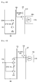
- Fig. 12 is a circuit diagram showing current flows when the circuit diagram of Fig. 10 is in an operation mode, the first switch P1 and the third switch N2 operate in a saturation area of the transistor, and the second switch N1 operates in a linear area of the transistor.
- a device (not shown) for amplifying the current difference may be further included in the front end of the input terminal of the output multiplexer 600a.
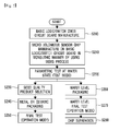
- resistance values of the reference cell 610 and the active cell 620 are measured respectively and a statistical monitoring is performed. It is judged whether the sensor is defective or not, and then a good die is selected.
Landscapes
- Physics & Mathematics (AREA)
- General Physics & Mathematics (AREA)
- Spectroscopy & Molecular Physics (AREA)
- Photometry And Measurement Of Optical Pulse Characteristics (AREA)
- Semiconductor Integrated Circuits (AREA)
- Solid State Image Pick-Up Elements (AREA)
Applications Claiming Priority (2)
| Application Number | Priority Date | Filing Date | Title |
|---|---|---|---|
| KR1020110019687A KR20120100643A (ko) | 2011-03-04 | 2011-03-04 | Sa-FPA를 이용한 적외선 감지기 및 이의 제조 방법 |
| PCT/KR2012/001612 WO2012121526A2 (fr) | 2011-03-04 | 2012-03-05 | Puce de capteur infrarouge, détecteur infrarouge et procédé de fonctionnement et procédé de test de ceux-ci |
Publications (2)
| Publication Number | Publication Date |
|---|---|
| EP2546623A2 true EP2546623A2 (fr) | 2013-01-16 |
| EP2546623A4 EP2546623A4 (fr) | 2014-07-23 |
Family
ID=46798638
Family Applications (1)
| Application Number | Title | Priority Date | Filing Date |
|---|---|---|---|
| EP12748373.3A Withdrawn EP2546623A4 (fr) | 2011-03-04 | 2012-03-05 | Puce de capteur infrarouge, detecteur infrarouge et procede de fonctionnement et procede de test de ceux-ci |
Country Status (5)
| Country | Link |
|---|---|
| US (1) | US20140014827A1 (fr) |
| EP (1) | EP2546623A4 (fr) |
| KR (2) | KR20120100643A (fr) |
| CN (1) | CN103026193B (fr) |
| WO (1) | WO2012121526A2 (fr) |
Cited By (2)
| Publication number | Priority date | Publication date | Assignee | Title |
|---|---|---|---|---|
| WO2014093724A1 (fr) * | 2012-12-14 | 2014-06-19 | Flir Systems, Inc. | Architecture de matrice en plan focal segmentée |
| US9918023B2 (en) | 2010-04-23 | 2018-03-13 | Flir Systems, Inc. | Segmented focal plane array architecture |
Families Citing this family (5)
| Publication number | Priority date | Publication date | Assignee | Title |
|---|---|---|---|---|
| US9948878B2 (en) | 2010-04-23 | 2018-04-17 | Flir Systems, Inc. | Abnormal clock rate detection in imaging sensor arrays |
| FR3009388B1 (fr) * | 2013-07-30 | 2015-07-17 | Ulis | Diagnostic de l'etat defectueux d'une matrice de detection bolometrique |
| CN104269465B (zh) * | 2014-09-30 | 2016-12-07 | 中国空空导弹研究院 | 焦平面探测器相连缺陷元的识别方法与测试基片 |
| JP7147468B2 (ja) * | 2018-10-26 | 2022-10-05 | 富士通株式会社 | 赤外線検出器の読み出し回路及びその検査方法 |
| KR102450595B1 (ko) * | 2020-10-26 | 2022-10-07 | 삼성전기주식회사 | 적외선 이미지 센서 및 적외선 카메라 모듈 |
Family Cites Families (8)
| Publication number | Priority date | Publication date | Assignee | Title |
|---|---|---|---|---|
| US5808350A (en) * | 1997-01-03 | 1998-09-15 | Raytheon Company | Integrated IR, visible and NIR sensor and methods of fabricating same |
| WO2006122529A2 (fr) * | 2005-05-17 | 2006-11-23 | Heimann Sensor Gmbh | Reseau de capteurs a infrarouge a thermopile |
| KR100765158B1 (ko) * | 2006-02-16 | 2007-10-15 | 주식회사 오카스 | 적외선 신호 검출 회로 및 검출 방법 |
| EP2034285B1 (fr) * | 2006-05-24 | 2013-04-03 | The Ritsumeikan Trust | Capteur à barrettes infrarouge |
| JP4978501B2 (ja) * | 2008-02-14 | 2012-07-18 | 日本電気株式会社 | 熱型赤外線検出器及びその製造方法 |
| FR2936052B1 (fr) * | 2008-09-16 | 2014-09-05 | Ulis | Dispositif pur la detection d'un rayonnement infrarouge comportant un bolometre resistif d'imagerie, systeme comprenant une matrice de tels bolometres, et procede de lecture d'un bolometre d'imagerie integre dans un tel system |
| CA2767023C (fr) * | 2011-02-09 | 2014-09-09 | Research In Motion Limited | Accroissement de la sensibilite de capteurs d'image dans des conditions d'eclairage a faible luminosite en combinant la sensibilite des points quantiques a la lumiere visible et aux infrarouges |
| US8436305B1 (en) * | 2011-03-16 | 2013-05-07 | Magnolia Optical Technologies, Inc. | Infrared radiation sensing device using a carbon nanotube and polymer composition and method of making the same |
-
2011
- 2011-03-04 KR KR1020110019687A patent/KR20120100643A/ko active Pending
-
2012
- 2012-03-05 CN CN201280000480.0A patent/CN103026193B/zh active Active
- 2012-03-05 WO PCT/KR2012/001612 patent/WO2012121526A2/fr not_active Ceased
- 2012-03-05 EP EP12748373.3A patent/EP2546623A4/fr not_active Withdrawn
- 2012-03-05 KR KR1020137009494A patent/KR101519607B1/ko active Active
- 2012-03-05 US US13/997,262 patent/US20140014827A1/en not_active Abandoned
Cited By (3)
| Publication number | Priority date | Publication date | Assignee | Title |
|---|---|---|---|---|
| US9918023B2 (en) | 2010-04-23 | 2018-03-13 | Flir Systems, Inc. | Segmented focal plane array architecture |
| US11070747B2 (en) | 2010-04-23 | 2021-07-20 | Flir Systems, Inc. | Segmented focal plane array architecture |
| WO2014093724A1 (fr) * | 2012-12-14 | 2014-06-19 | Flir Systems, Inc. | Architecture de matrice en plan focal segmentée |
Also Published As
| Publication number | Publication date |
|---|---|
| KR20120100643A (ko) | 2012-09-12 |
| KR101519607B1 (ko) | 2015-05-15 |
| CN103026193B (zh) | 2017-04-05 |
| KR20130057482A (ko) | 2013-05-31 |
| CN103026193A (zh) | 2013-04-03 |
| US20140014827A1 (en) | 2014-01-16 |
| WO2012121526A3 (fr) | 2012-12-27 |
| EP2546623A4 (fr) | 2014-07-23 |
| WO2012121526A2 (fr) | 2012-09-13 |
Similar Documents
| Publication | Publication Date | Title |
|---|---|---|
| EP2546623A2 (fr) | Puce de capteur infrarouge, detecteur infrarouge et procede de fonctionnement et procede de test de ceux-ci | |
| TWI439711B (zh) | 切換矩陣器及其半導體元件特性之測試系統 | |
| WO2020135258A1 (fr) | Puce d'essai adressable susceptible d'améliorer la précision de mesure de résistance et son système d'essai | |
| WO2020135257A1 (fr) | Puce de test adressable et système apte à réduire le courant de fuite | |
| US8040152B1 (en) | Separate configuration of I/O cells and logic core in a programmable logic device | |
| KR100485462B1 (ko) | 집적회로검사방법 | |
| US6259267B1 (en) | Power-current measuring circuit in burn-in tester | |
| JP5193635B2 (ja) | 半導体装置 | |
| TWI683113B (zh) | 用於裝置的測試器、操作開關電路的方法、以及測試裝置的方法 | |
| US9824945B2 (en) | Semiconductor device and semiconductor device measuring method | |
| US20130300497A1 (en) | Reconfigurable integrated circuit | |
| US7844874B2 (en) | Semiconductor integrated circuit device and inspection method therefor | |
| JPWO2006080111A1 (ja) | 半導体集積回路及びシステムlsi | |
| US20090212812A1 (en) | Multi-chip package semiconductor device and method of detecting a failure thereof | |
| US20240414453A1 (en) | Image sensor with temperature sensing pixels | |
| US20060170433A1 (en) | Semiconductor test circuit | |
| JP2011222547A (ja) | テストエレメントグループおよび半導体装置 | |
| JP2009133762A (ja) | 半導体装置およびその試験方法 | |
| JP7392533B2 (ja) | 検査システム | |
| JP2010190839A (ja) | 半導体装置 | |
| JP4480880B2 (ja) | 半導体回路 | |
| JP2009065037A (ja) | 半導体集積回路とその検査装置 | |
| JP2012249007A (ja) | 出力回路及びそのドライブ能力テスト方法。 | |
| JP2010223791A (ja) | 半導体装置及びその検査方法 | |
| KR100787098B1 (ko) | 센서칩을 포함하는 다중칩 패키지의 테스트회로 및 그테스트 회로를 포함하는 다중칩 패키지 |
Legal Events
| Date | Code | Title | Description |
|---|---|---|---|
| PUAI | Public reference made under article 153(3) epc to a published international application that has entered the european phase |
Free format text: ORIGINAL CODE: 0009012 |
|
| 17P | Request for examination filed |
Effective date: 20120829 |
|
| AK | Designated contracting states |
Kind code of ref document: A2 Designated state(s): AL AT BE BG CH CY CZ DE DK EE ES FI FR GB GR HR HU IE IS IT LI LT LU LV MC MK MT NL NO PL PT RO RS SE SI SK SM TR |
|
| R17D | Deferred search report published (corrected) |
Effective date: 20121227 |
|
| RIN1 | Information on inventor provided before grant (corrected) |
Inventor name: KIM, GYUNG TAE Inventor name: PARK, JAE HONG Inventor name: KIM, HEE YEOUN Inventor name: LEE, KWY RO Inventor name: KIM, BYEONG IL Inventor name: KIM, KYOUNG MIN Inventor name: KYUNG, KI MYEONG |
|
| DAX | Request for extension of the european patent (deleted) | ||
| A4 | Supplementary search report drawn up and despatched |
Effective date: 20140623 |
|
| RIC1 | Information provided on ipc code assigned before grant |
Ipc: H01L 31/101 20060101ALI20140616BHEP Ipc: G01J 5/02 20060101AFI20140616BHEP Ipc: G01J 5/20 20060101ALI20140616BHEP |
|
| STAA | Information on the status of an ep patent application or granted ep patent |
Free format text: STATUS: THE APPLICATION IS DEEMED TO BE WITHDRAWN |
|
| 18D | Application deemed to be withdrawn |
Effective date: 20141001 |