EP2548058B1 - Réseau de diffraction à guides d'onde compensé en température jusqu'au deuxième ordre comprenant des fentes longitudinales - Google Patents
Réseau de diffraction à guides d'onde compensé en température jusqu'au deuxième ordre comprenant des fentes longitudinales Download PDFInfo
- Publication number
- EP2548058B1 EP2548058B1 EP11711225.0A EP11711225A EP2548058B1 EP 2548058 B1 EP2548058 B1 EP 2548058B1 EP 11711225 A EP11711225 A EP 11711225A EP 2548058 B1 EP2548058 B1 EP 2548058B1
- Authority
- EP
- European Patent Office
- Prior art keywords
- waveguide
- core
- compensation
- temperature
- slots
- Prior art date
- Legal status (The legal status is an assumption and is not a legal conclusion. Google has not performed a legal analysis and makes no representation as to the accuracy of the status listed.)
- Not-in-force
Links
- 239000000463 material Substances 0.000 claims description 103
- 230000003287 optical effect Effects 0.000 claims description 63
- 239000011162 core material Substances 0.000 claims description 57
- 238000000034 method Methods 0.000 claims description 38
- 238000005253 cladding Methods 0.000 claims description 20
- 238000004519 manufacturing process Methods 0.000 claims description 6
- VYPSYNLAJGMNEJ-UHFFFAOYSA-N Silicium dioxide Chemical group O=[Si]=O VYPSYNLAJGMNEJ-UHFFFAOYSA-N 0.000 description 43
- 239000002131 composite material Substances 0.000 description 42
- 229920000642 polymer Polymers 0.000 description 30
- 239000000377 silicon dioxide Substances 0.000 description 20
- 230000008859 change Effects 0.000 description 19
- 238000013461 design Methods 0.000 description 7
- 230000000694 effects Effects 0.000 description 7
- 238000002834 transmittance Methods 0.000 description 7
- 239000011521 glass Substances 0.000 description 6
- 238000012986 modification Methods 0.000 description 6
- 230000004048 modification Effects 0.000 description 6
- 238000004891 communication Methods 0.000 description 5
- 238000007796 conventional method Methods 0.000 description 5
- 230000007423 decrease Effects 0.000 description 5
- 239000000835 fiber Substances 0.000 description 5
- 230000010287 polarization Effects 0.000 description 5
- 230000001419 dependent effect Effects 0.000 description 4
- 238000009826 distribution Methods 0.000 description 4
- 230000003595 spectral effect Effects 0.000 description 4
- 239000000758 substrate Substances 0.000 description 4
- 230000005540 biological transmission Effects 0.000 description 3
- 230000008878 coupling Effects 0.000 description 3
- 238000010168 coupling process Methods 0.000 description 3
- 238000005859 coupling reaction Methods 0.000 description 3
- 239000012467 final product Substances 0.000 description 3
- 238000003780 insertion Methods 0.000 description 3
- 230000037431 insertion Effects 0.000 description 3
- 239000013307 optical fiber Substances 0.000 description 3
- 230000004044 response Effects 0.000 description 3
- 238000004458 analytical method Methods 0.000 description 2
- 230000008901 benefit Effects 0.000 description 2
- 238000005229 chemical vapour deposition Methods 0.000 description 2
- 238000000151 deposition Methods 0.000 description 2
- 238000005530 etching Methods 0.000 description 2
- 238000010438 heat treatment Methods 0.000 description 2
- 230000006872 improvement Effects 0.000 description 2
- 238000006386 neutralization reaction Methods 0.000 description 2
- 238000004806 packaging method and process Methods 0.000 description 2
- 230000008569 process Effects 0.000 description 2
- XUIMIQQOPSSXEZ-UHFFFAOYSA-N Silicon Chemical compound [Si] XUIMIQQOPSSXEZ-UHFFFAOYSA-N 0.000 description 1
- 239000000969 carrier Substances 0.000 description 1
- 229910052681 coesite Inorganic materials 0.000 description 1
- 238000010276 construction Methods 0.000 description 1
- 238000012937 correction Methods 0.000 description 1
- 229910052906 cristobalite Inorganic materials 0.000 description 1
- 125000004122 cyclic group Chemical group 0.000 description 1
- 230000008021 deposition Effects 0.000 description 1
- 230000001747 exhibiting effect Effects 0.000 description 1
- 238000001914 filtration Methods 0.000 description 1
- 230000008014 freezing Effects 0.000 description 1
- 238000007710 freezing Methods 0.000 description 1
- 229910052732 germanium Inorganic materials 0.000 description 1
- GNPVGFCGXDBREM-UHFFFAOYSA-N germanium atom Chemical compound [Ge] GNPVGFCGXDBREM-UHFFFAOYSA-N 0.000 description 1
- 230000007062 hydrolysis Effects 0.000 description 1
- 238000006460 hydrolysis reaction Methods 0.000 description 1
- 230000002401 inhibitory effect Effects 0.000 description 1
- 238000002955 isolation Methods 0.000 description 1
- 238000012886 linear function Methods 0.000 description 1
- 238000013507 mapping Methods 0.000 description 1
- 238000010297 mechanical methods and process Methods 0.000 description 1
- 239000002861 polymer material Substances 0.000 description 1
- 229920001296 polysiloxane Polymers 0.000 description 1
- -1 polysiloxanes Polymers 0.000 description 1
- 239000000047 product Substances 0.000 description 1
- 230000001902 propagating effect Effects 0.000 description 1
- 230000005855 radiation Effects 0.000 description 1
- 238000012552 review Methods 0.000 description 1
- 230000035945 sensitivity Effects 0.000 description 1
- 229910052710 silicon Inorganic materials 0.000 description 1
- 239000010703 silicon Substances 0.000 description 1
- 238000004088 simulation Methods 0.000 description 1
- 238000004544 sputter deposition Methods 0.000 description 1
- 229910052682 stishovite Inorganic materials 0.000 description 1
- 238000011071 total organic carbon measurement Methods 0.000 description 1
- 229910052905 tridymite Inorganic materials 0.000 description 1
Images










Classifications
-
- G—PHYSICS
- G02—OPTICS
- G02B—OPTICAL ELEMENTS, SYSTEMS OR APPARATUS
- G02B6/00—Light guides; Structural details of arrangements comprising light guides and other optical elements, e.g. couplings
- G02B6/10—Light guides; Structural details of arrangements comprising light guides and other optical elements, e.g. couplings of the optical waveguide type
- G02B6/12—Light guides; Structural details of arrangements comprising light guides and other optical elements, e.g. couplings of the optical waveguide type of the integrated circuit kind
- G02B6/12007—Light guides; Structural details of arrangements comprising light guides and other optical elements, e.g. couplings of the optical waveguide type of the integrated circuit kind forming wavelength selective elements, e.g. multiplexer, demultiplexer
- G02B6/12009—Light guides; Structural details of arrangements comprising light guides and other optical elements, e.g. couplings of the optical waveguide type of the integrated circuit kind forming wavelength selective elements, e.g. multiplexer, demultiplexer comprising arrayed waveguide grating [AWG] devices, i.e. with a phased array of waveguides
- G02B6/12011—Light guides; Structural details of arrangements comprising light guides and other optical elements, e.g. couplings of the optical waveguide type of the integrated circuit kind forming wavelength selective elements, e.g. multiplexer, demultiplexer comprising arrayed waveguide grating [AWG] devices, i.e. with a phased array of waveguides characterised by the arrayed waveguides, e.g. comprising a filled groove in the array section
-
- G—PHYSICS
- G02—OPTICS
- G02B—OPTICAL ELEMENTS, SYSTEMS OR APPARATUS
- G02B6/00—Light guides; Structural details of arrangements comprising light guides and other optical elements, e.g. couplings
- G02B6/10—Light guides; Structural details of arrangements comprising light guides and other optical elements, e.g. couplings of the optical waveguide type
- G02B6/12—Light guides; Structural details of arrangements comprising light guides and other optical elements, e.g. couplings of the optical waveguide type of the integrated circuit kind
- G02B6/12007—Light guides; Structural details of arrangements comprising light guides and other optical elements, e.g. couplings of the optical waveguide type of the integrated circuit kind forming wavelength selective elements, e.g. multiplexer, demultiplexer
- G02B6/12009—Light guides; Structural details of arrangements comprising light guides and other optical elements, e.g. couplings of the optical waveguide type of the integrated circuit kind forming wavelength selective elements, e.g. multiplexer, demultiplexer comprising arrayed waveguide grating [AWG] devices, i.e. with a phased array of waveguides
- G02B6/12026—Light guides; Structural details of arrangements comprising light guides and other optical elements, e.g. couplings of the optical waveguide type of the integrated circuit kind forming wavelength selective elements, e.g. multiplexer, demultiplexer comprising arrayed waveguide grating [AWG] devices, i.e. with a phased array of waveguides characterised by means for reducing the temperature dependence
- G02B6/12028—Light guides; Structural details of arrangements comprising light guides and other optical elements, e.g. couplings of the optical waveguide type of the integrated circuit kind forming wavelength selective elements, e.g. multiplexer, demultiplexer comprising arrayed waveguide grating [AWG] devices, i.e. with a phased array of waveguides characterised by means for reducing the temperature dependence based on a combination of materials having a different refractive index temperature dependence, i.e. the materials are used for transmitting light
Definitions
- the present invention relates generally to optical grating devices, and more particularly to techniques for athermalizing such devices.
- WDM wavelength division multiplexed
- Fiber-optic multiplexing and demultiplexing have been accomplished using an arrayed waveguide grating (AWG) device.
- AWG is a planar structure comprising an array of waveguides disposed between input and output couplers and arranged side-by-side with each other, and which together act like a diffraction grating in a spectrometer.
- Each of the waveguides differs in length with respect to its nearest neighbor by a predetermined fixed amount.
- the outputs of the output coupler form the outputs of the multiplexing and demultiplexing device. In operation, when a plurality of separate and distinct wavelengths are applied to separate and distinct input ports of the device, they are combined and are transmitted to an output port.
- the same device may also perform a demultiplexing function in which a plurality of input wavelengths on one input port of the apparatus, are separated from each other and directed to predetermined different ones of the output ports.
- AWGs can also perform a routing function, in which signals arrive on multiple input ports and are routed to multiple different output ports in accordance with a predefined mapping.
- the construction and operation of such AWGs is well known in the art. See for example, " PHASAR-based WDM-devices: Principles, Design and Applications", M K Smit, IEEE Journal of Selected Topics in Quantum Electronics Vol. 2, No. 2 June 1996 , and U.S. Pat. No. 5,002,350 and WO97/23969 .
- Wavelength division multiplexers and demultiplexers require precise control of the effective optical path length difference between adjacent waveguides.
- the effective optical path length difference is defined as the product of the effective index of refraction of the fundamental mode in the waveguide and the physical path length difference between adjacent waveguides.
- the effective index of refraction of the fundamental mode in the waveguides and the physical path length differences between adjacent waveguides for currently available wavelength division multiplexers and demultiplexers are typically both temperature dependent.
- the medium forming the arrayed waveguides has a noticeable temperature dependency which results in changes in the central transmission wavelength which may exceed the transmission bandwidth. As a result, temperature variations that are within a specified device operating temperature range (e.g.
- multiplexer/demultiplexer optical devices of the phased array type are generally operated in a temperature controlled environment.
- control circuits with heating elements are provided to maintain the device at a stable temperature higher than the maximum specified operating temperature.
- heating elements to achieve active athermalization is undesirable because it increases the overall cost, size and complexity of the device, reduces device lifetimes, and consumes considerable power. It also usually requires active smart control electronics and even then it may operate differently depending on the device's physical horizontal/vertical orientation.
- Peltier coolers can also be used, but these suffer from many of the same inadequacies.
- the variation of channel wavelength as a function of temperature predominately depends on the positive variation of the effective index of refraction of the silica as a function of temperature.
- polymer overcladding materials having a negative variation of refractive index as a function of temperature have been employed.
- a problem with this arrangement is that as the temperature varies, the difference in refractive index between the core and the cladding varies, and in the worst case, light may not be able to be guided into the waveguide.
- optical multiplexer/demultiplexer devices having a phased array type grating with a polymer overcladding may not be suitable for use over a wide range of ambient temperatures.
- Another proposed design for maintaining a relatively constant effective optical path length difference between adjacent waveguides in a phased array involves localizing a compensation material (typically a polymer) in a triangular or crescent-shaped groove or slot either in the phased array or in the slab region coupling the phased array with either the input or output fibers.
- the polymer-filled groove is transversely oriented across adjacent waveguides in a direction generally perpendicular to the direction of the optical paths.
- the physical length of the groove along the optical path of a given waveguide is a function of the physical path length, such that the optical paths of adjacent waveguides experience a constant physical path length increment through the groove.
- the polymer can be selected such that it has a negative variation in effective index of refraction as a function of temperature to compensate for the positive variation in the index of refraction of the silica waveguide core segments as a function of temperature, thereby inhibiting shifting of channel wavelengths due to variations in operating temperature within a predetermined operating temperature range.
- the polymer groove can be divided into more than one groove encountered by the optical energy sequentially, to reduce the length of free space propagation across each groove.
- polymer-filled grooves can improve athermalization substantially.
- the change in the respective index of refraction of each of the silica based waveguide and the polymer compensation material are both assumed to be linear with temperature. Any higher order effects typically are ignored.
- Typical AWGs that have been athermalized in this way can achieve a center channel wavelength drift as small as 0.03 to 0.05 nm over a typical operating temperature range of +5 to +70 C. However, that is still not good enough for many applications. Such drifts limit the applicability of the device to only that stated temperature range, and to only systems having channel spacings of about 100 GHz or higher, where this variation would be tolerable. They are not readily usable, for example, in an outdoor equipment enclosure in climates where freezing temperatures are possible, or in systems that require a broad passband and a channel spacing less than about 100GHz.
- Another major category of techniques that have been investigated for athermalization are mechanical in nature, such as techniques that include temperature-controlled actuators for actively positioning the components of the device relative to each other. These may include, for example, a bi-metallic actuator that adjusts the lateral position of the input waveguide relative to the input slab region in accordance with ambient temperature. These techniques are generally complex and expensive to make as the manufacturing tolerances are usually extremely tight.
- EP 1 089 098 A1 discloses an athermalized optical waveguide circuit device exhibiting reduced signal power losses includes an optical phased-array comprising a plurality of curved waveguide cores of different lengths supported on a planar substrate, wherein each of the waveguide cores of the array includes a first silica segment, a second silica segment, and a central polymer segment connecting the first silica segment with the second silica segment to form a continuous waveguide core.
- US2008/226232 A1 describes an optical apparatus with an improved center wavelength temperature stability.
- US2008/226232 A1 further describes an AWG with a plurality of slots inserted along the optical paths.
- the slots contain one or more compensation materials which collectively correct for an order Q temperature dependency of the AWG base material.
- a compensation material within slot elongated in a direction parallel to a segment of waveguide in an arrayed waveguide grating apparatus can compensate for both first and second order change in refractive index of the base waveguide material over temperature.
- the elongated slot generally parallel to the base material defines a composite waveguide section having a second order effective index of refraction temperature dependency which can be utilized to accurately minimize the temperature dependence of the overall optical path length to both the first and second order.
- the techniques described herein are also generalizeable to neutralization of the optical path length temperature dependence to any order. As a result, the techniques described herein can compensate for the effective optical path length variation in the waveguide material with much better accuracy, or over a much wider temperature range of -30 C to +70C for example, or both.
- An arrayed waveguide apparatus as described herein includes a plurality of waveguides from an input free-space region to an output free-space region, the input free space region having an input port and the output free space region having an output port.
- Each waveguide in the plurality comprises a core material, a cladding material, and a compensation material within a slot elongated in a direction parallel to the core material. The slot being parallel to a segment of the core material.
- the compensation material has an effective index of refraction temperature dependency with differs from that of the core and cladding materials.
- the compensation material is selected and the slot is arranged such that at least the second order derivative with respect to temperature of a center wavelength of the arrayed waveguide apparatus from the input port to the output port is substantially equal to zero throughout a temperature range of -5°C to +70°C
- An arrayed waveguide apparatus as described herein includes a plurality of waveguides from an input free-space region to an output free-space region.
- Each waveguide in the plurality includes core and cladding materials which confine optical energy in at least one dimension orthogonal to a direction of propagation of the optical energy.
- Each waveguide further includes a composite waveguide section which maintains confinement of the optical energy in the at least one dimension.
- Each waveguide has a respective optical path length between an input boundary of the input free-space region and output boundary of the output free-space region which differs from that of an adjacent waveguide in the plurality by a respective effective optical path length difference.
- Each optical path may further include a section of transverse slots as in the conventional liner athermal AWG described before. At least the first and second order derivatives with respect to temperature for each of the optical path length differences are substantially equal to zero throughout a temperature range of -5 degrees Celsius to +70 degrees Celsius.
- Fig. 1 illustrates the spectral response of a typical AWG acting as a wavelength division demultiplexer.
- the plot illustrates the transmittance observed at each of a plurality of different output channels, all superimposed onto a single plot.
- the plot illustrates the spectral response of a typical AWG acting as a wavelength division multiplexer, with the transmittance from each of a plurality of different input channels to a common output superimposed onto a single plot.
- Each transmittance curve has a main lobe that peaks at about -5 dB in this example, and has a center f c that varies incrementally from channel to channel, with substantially equal spacing between the center frequencies of adjacent channels. The center frequencies need not be spaced equally in different AWG embodiments.
- the center wavelength ⁇ c is defined herein as the average of the two wavelengths for which the transmittance is half the peak transmittance for average polarization state.
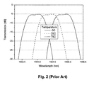
- Fig. 2 is a plot showing the transmittance in a single channel of a conventional AWG, at ambient temperatures of -5 C, +35 C and +75 C. It can be seen that the center wavelength increases as the temperature increases. The center wavelength variation with temperature is approximately the same for each channel, so analysis of the center wavelength variation for one channel for most AWG designs is representative of all channels in the design. For purposes of the present discussion, the central channel is used at both the input and output. This center wavelength shift with temperature is problematic in mux/demux applications because the wavelength of the incoming optical energy does not shift.
- the incoming optical energy for a given channel has the great majority of its power concentrated within the main lobe of the corresponding AWG passband, so as the passband shifts in wavelength, the channel loss can become substantial. It can be seen that losses may be acceptable above a predetermined channel wavelength spacing (permitting an AWG designed with wider passbands), but unacceptable for narrower channel spacings (requiring an AWG designed with narrow passbands). In filtering applications, a shift in the central wavelength of the passbands can cause the resulting signal to be out of specification and inappropriate for downstream components.
- n eff is the effective index of refraction in the waveguide
- ⁇ L is the length increment between adjacent waveguides in the array
- m is the order of the grating.
- the temperature dependence of the center wavelength ⁇ c arises because both n eff and ⁇ L vary with temperature, although the temperature dependence of n eff is typically much more significant. In fact as explained below, the temperature dependence of ⁇ L can be lumped into that of n eff without losing much accuracy.
- Each material is therefore characterized with two index of refraction terms, a 0'th order term n 0x , and a first order term n 1x .
- Fig. 4 is a plot showing the measured center wavelength temperature dependency of an AWG made according to this linearly athermalized technique. As can be seen in Fig. 4 , significant center wavelength variation remains in the linearly athermalized AWG.
- the second order coefficient ⁇ 2 e can be represented mathematically as the sum of a second order coefficient ⁇ 2 g due to the silica and a second order coefficient ⁇ 2 p due to the polymer.
- ⁇ 2 e is approximately 2.5E-05 nm/C/C, with ⁇ 2 g being about 1.5E-05 nm/C/C and ⁇ 2 p being about 1.0E-05 nm/C/C.
- Fig. 5 is a plot showing the measured effective second order wavelength variation coefficient ⁇ 2 e various waveguides which have been linearly athermalized using different sample polymers. As can be seen in Fig. 5 , the linearly athermalized waveguides exhibit nearly identical thermo-optic curvature characteristics regardless of the polymer used.
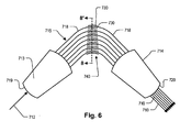
- Fig. 6 illustrates an AWG wavelength division multiplexer/de-multiplexer that has been athermalized utilizing slots 730 elongated in a direction parallel to the waveguides by taking second order temperature dependencies into account. It comprises a substrate or "die” (not shown) having provided thereon an arrayed waveguide grating 715 (also called a prism region) comprising an array of channel waveguides 718, only some of which are shown, which are optically coupled between two planar (slab or free-space) waveguide coupling regions 713 and 714.
- an arrayed waveguide grating 715 also called a prism region
- At least input waveguide 712 is optically coupled to an input face (or boundary) 719 of the first slab waveguide 713 for inputting a multiplexed input signal thereto, and a plurality of output waveguides 710 (only some shown) are optically coupled to an output face (or boundary) 720 of the second slab waveguide 714 for outputting respective wavelength channel outputs therefrom to the face 720.
- the input and output waveguides 712 and 710 preferably are integrated on the same die as the grating 715 and the two coupling regions 713 and 714, but in another embodiment they can be optical fibers, for example, or lens systems.
- the geometries of the slab waveguide regions 713 and 714 are both well known, and described for example in U.S. Patent No. 6,768,842 .
- the physical length of the waveguides increases incrementally by the same amount from one waveguide to the next.
- the effective optical path length difference ⁇ L x determines the position of the different wavelength output channels on the output face 720 of the second slab waveguide 714.
- the physical length of the waveguides in the array increases incrementally by the same amount, ⁇ L g , from one waveguide to the next.
- the slots 730 are filled with a compensation material and are elongated in a direction parallel to the core of the waveguides 418.
- the term “material” can be made up of one or more other materials, either mixed together, or layered, or combined in some other manner to make the overall "material.”
- the slots 730 are shaped and sized to define composite waveguide sections 740 having a second order effective index of refraction temperature dependency which minimizes the temperature dependence of the overall optical path length to both the first and second order.
- composite waveguide section refers to a stretch of waveguide that is influenced by the slots alongside it.
- the device in Fig. 6 is athermalized by taking into account the first and second order temperature dependency of the composite waveguide sections 740 and the first and second order temperature dependency of the remaining waveguide sections (or non-parallel-slotted sections).
- ⁇ c n c ⁇ ⁇ ⁇ L c + n r ⁇ ⁇ ⁇ L r m
- n c is the effective index of refraction of each of the composite waveguide sections 740
- ⁇ L c is the increment between adjacent waveguides in the operative length of the composite waveguide sections 730 encountered longitudinally by the optical energy
- n r is the effective index of refraction of the remaining sections of the waveguides
- ⁇ L r is the increment between adjacent waveguides in the total physical length of the remaining non-composite sections of the waveguides encountered longitudinally by the optical energy.
- ⁇ L x is therefore given by the sum of ⁇ L c and ⁇ L r .
- the remaining non-composite sections of waveguide provide conventional linear athermalization as described above.
- the operative length increment ⁇ L c of the composite waveguide sections 730 depends on the proximity, shape and materials within the slots 730, along with other factors.
- the operative length increment ⁇ L c is thus not necessarily the increment between adjacent waveguides in the physical length of the slots 730.
- the operative length increment ⁇ L c is intended to reflect a lumped measure which takes into account the variations in the amount of influence on the optical energy flow that the slot 730 has along its length. It does not matter, for the purposes of this discussion, how the operative length of the composite waveguide sections 730 are calculated, so long as the same method is used for all waveguides 718.
- the first and second order dependencies of the effective index of refraction n r of the non-parallel slotted sections will depend on the first and second order terms for the index of refraction of polymer and glass, as well as the polymer to glass path length ratio ⁇ L p / ⁇ L g . Then, by appropriate design of the size, shape and material(s) for the slots 730, along with the index and path length increment of the operative length increment ⁇ L c , the effective index of refraction n c of the composite waveguide sections 740 can be designed to satisfy both (eq. 23) and (eq. 24).
- second order athermalization is achieved due to the first and second order temperature dependency of the effective index of refraction n c of the composite waveguide sections 740, which counters the first and second order temperature dependency of the effective index of refraction n r of the remaining waveguide sections.
- the compensation material within the slots 730 has an effective index of refraction temperature dependency with differs from that of the core and cladding materials of the channel waveguides 718.
- at least three variables can be adjusted to design parallel slots 730 which satisfy both (eq. 23) and (eq. 24) as described herein.
- a stronger decrease in the overall effective wavelength curvature i.e. second order temperature dependency
- a weaker decrease can be obtained by choosing a compensation material which exhibits a lower index of refraction at a given temperature.
- a stronger effect on the overall effective wavelength curvature can be obtained by disposing the slots 730 closer to the core centerlines of the waveguides 718.
- a weaker effect can be obtained by disposing the slots 730 farther from the core centerlines. Both of these variables operate by affecting the optical mode profile through modification of the light distribution in the composite waveguide section 740 versus temperature, as discussed in more detail below.
- a stronger effect can be obtained by designing the slots 730 using a larger ⁇ L c
- a weaker effect can be obtained by designing them using a smaller ⁇ L c .
- ⁇ L r and the index of refraction n r of the remaining waveguide sections can be adjusted. A designer can then vary the above variables until the net curvature of the wavelength temperature dependence throughout a desired temperature range is minimized.
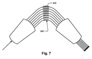
- the slots 730 have lengths that occupy a longer segment of the channel waveguides 718 that they straddle, for progressively shorter waveguides 718. This is appropriate in order to satisfy (eq. 22). According to that equation, if n 1c and n 1r are of the same sign, the equations can be satisfied only if the operative length increment ⁇ L c of the composite waveguide sections 740 is of the opposite sign as the increment ⁇ L r of the non-parallel slotted sections. In addition, in preferred embodiments n 1c is designed to be smaller than n 1r , so that the slots 730 do not have to be as long or longer than the branch waveguides 718. In another embodiment, as shown in Fig.
- the composite waveguide sections 840 can have an effective index of refraction variation with temperature which is of the opposite sign as that of the remaining waveguide sections.
- the slots 830 have lengths that occupy a longer segment of the channel waveguides 840 that they straddle, for progressively longer waveguides.
- Fig. 8 is a cross-section of a portion of the channel waveguides 718, taken along the sight lines 8-8' in Fig. 6 .
- Each of the waveguides 718 includes a core material 810 within a cladding material 800.
- each of the waveguides 718 includes a pair of slots 730 straddling the core material 810.
- the slots 730 do not cross into the core region of the waveguides 718.
- the slots 730 do cross into the core region of the waveguide 718.
- the core material 810 is Germanium doped glass with a refractive index of about 1.47 and has a square-cross section with a width 1000 of 4 ⁇ m.
- the core material 810 is surrounded by a glass cladding 800 having a refractive index of about 1.45.
- the slots 730 have a width 1010 of 4.4 ⁇ m and a center-to-center distance 1020 between the pair of inserts 730 straddling a given core of 7.6 ⁇ m.
- Fig. 6 The structure of Fig. 6 can be fabricated using well-known techniques.
- the transmission waveguides 718 and slab waveguides 713, 714 are formed (e.g. using standard photolithographic techniques) as "cores" on a silicon substrate.
- An oxide layer and/or cladding layer may be provided on the substrate prior to depositing the waveguide cores.
- the cores are then covered in cladding material, using for example Flame Hydrolysis Deposition (FHD) or Chemical Vapor Deposition (CVD) fabrication processes.
- FHD Flame Hydrolysis Deposition
- CVD Chemical Vapor Deposition
- the slots 730 are then etched photolithographically, and the compensation material is applied using a volumetrically controlled syringe dispenser and then cured, either thermally or using actinic radiation depending on the choice of compensation material. Alternatively, the compensation material can be deposited into the slots 730 by sputtering or any other method.
- Fig. 10 is an image of a manufactured device having elongated slots
- the slots 730 elongated in a direction parallel to the waveguides act to maintain confinement of the optical energy carried in the remaining non-composite sections.
- confinement of the optical energy in this portion is lost. This is due to the fact that the optical energy is not guided by the material of the transverse slots.
- optical energy being guided by the waveguide which enters the transverse slots can propagate outwardly into the region surrounding waveguide where it cannot be recovered, rather than being coupled into the next section of waveguide.
- slots 730 elongated in a direction parallel to the waveguides as described herein maintain confinement of the optical energy in at least one dimension orthogonal to a direction of propagation of the optical energy.
- This confinement is due to the index contrast at the outermost sides of the slots 730 along the direction of propagation of the optical energy. Due to the differences between the cladding and compensation materials, this index contrast at the outermost interface between the compensation material and the cladding material provides substantially total internal reflection which provides confinement of the optical energy.
- optical energy within the compensation material can be coupled into the next section of waveguide, rather than being lost.
- core material 800 is adjacent to the left side of the left slot 730 and the right side of the right slot 730 of each waveguide 718.
- the optical energy is confined in the horizontal dimension.
- the slots 730 do not give rise to additional losses in the AWG. As described below, this can be achieved by designing the slots 730 to enter the path of the optical beams adiabatically, or nearly so.
- Fig. 11 is a top view of a portion of the channel waveguides 718 having small additional losses introduced by the slots 730.
- the slots 730 include proximal and distal ends and curve away from the core material 810 they straddle at both ends. This is one way of minimizing the loss as the optical energy in the waveguides 718 encounters the slots 730.
- each of the slots is shown curving to the point where it meets the near slot for the next adjacent waveguide 718. This can help minimize the loss because it maximizes the distance between the beginning of each slot 730 and the waveguide cores. In other embodiments, it is not necessary that the ends of the slots meet.
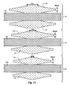
- Fig. 12 is a top view of a portion of another embodiment of the channel waveguides 718.
- the slots 730 instead curving the slots 730 away from the cores 810, the slots 730 have ends which are adiabatically tapered down to a width Wend.
- the gradual or adiabatic variation at the input and output sections of the slots 730 ensures that little to no optical light is scattered when the light in the waveguide 718 begin to interact with the slots 730.
- the lengths and widths of the adiabatic sections of the slots 730 can be chosen using for example beam propagation method (BPM) simulations to optimize the length and minimize loss.
- BPM beam propagation method
- the absolute lengths of the adiabatic sections should not affect the net curvature of the wavelength versus temperature curve of the waveguides 718, as long as the adiabatic sections have the same length in all the slots 730.
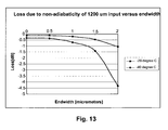
- Fig. 13 is a plot of the simulated insertion loss versus width Wend of the tapered slots 730. As shown in Fig. 13 , an insertion loss penalty of less than 0.5 dB can be achieved with a width Wend as large as 0.5 ⁇ m, even at -40 degrees C.
- Yet another way to minimize loss is to vary the depth of the slots 730 in the vertical dimension relative to the depth of the core material 810, or the thickness of the slots 730 in the vertical dimension. In certain embodiments, these may be more difficult to achieve than tapering or curving away in transverse dimension, but may be appropriate for other embodiments.
- Figs. 14A-14C illustrate cross-sectional views of a portion of the channel waveguides 718 showing alternative configurations for the slots 730.
- the slots 730 have a relatively large width and are formed over the core material 810 of each of the waveguides 718. In such a case, the slot 730 for each waveguide 718 is discontiguous from the slots 730 of each of the other waveguides 718.
- the slots 730 have a width similar the width of the core material 810.
- each of the waveguides 718 includes a single slot 730 straddling one side of the core material 810.
- Fig. 15 illustrates an AWG device in which the elongated slots used for athermalization are segmented along the length of the waveguides.
- the waveguides 718 include first slots 730a elongated in a direction parallel to one longitudinal segment, and second slots 730b elongated in a direction parallel to another longitudinal segment.
- one or more of the size, shape and compensation material in the first slots 730a may be different from those in the second slots 730b.
- the first slots 730a may have a different cross-section than that the of the second slots 730b, for example being a different distance away from the core material of the waveguides 718.
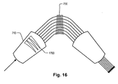
- Fig. 16 illustrates an AWG device which includes elongated slots 730 as described herein in conjunction with transversely oriented slots 1700 within the first slab waveguide 713.
- the transversely oriented slots 1700 provide conventional linear athermalization
- the elongated slots 730 provide the second order athermalization as described herein.
- the same compensation material may be used in both the elongated slots 730 and the transversely oriented slots 1700.
- different materials may be used.
- both compensation materials are polysiloxanes, with the compensation material in the transverse slots 1700 having an index or refraction of about 1.46, and the compensation material in the parallel elongated slots 730 has an index of refraction of 1.42.
- the slots 730 not only provide second order curvature correction, but also creates a change in the slope of the wavelength versus temperature curve at a given temperature.
- the strength of the athermalization by the slots 1700 may have to be adjusted in conjunction with that of the slots 730. This adjustment of both the slots 1700 and the slots 730 can be achieved using the techniques described mathematically above.
- second order athermalization is achieved by designing the second order temperature dependency of the effective index of refraction n c of the composite waveguide sections 740, to counter the second order temperature dependency of the effective index of refraction n r of the remaining waveguide sections.
- the principle in creating sufficient second order temperature dependency of the effective index of refraction n c of the composite waveguide sections 740, is achieved through modification of the light distribution in the composite waveguide sections 740 versus temperature.
- Figs. 17A-17D illustrate an example of the change in the cross-sectional light distribution versus temperature for an exemplary composite waveguide section 740 having a cross-section like that shown in Fig. 8 .
- the index of refraction of the compensation material in the slots 730 increases as the temperature decreases.
- This increase in the index of refraction of the compensation material will itself increase effective index of refraction of the composite waveguide section 740, because a certain percentage of the light is traveling through the slots 730.
- the light will redistribute itself towards this higher index of refraction region, the slots 730, with the change in temperature. This redistribution also acts to increase the effective index of refraction of the composite waveguide section 740, resulting in a 2nd order effect.
- Fig. 18 is a plot of an example of a calculated effective index of refraction n c versus temperature for an exemplary composite waveguide section having a silica core.
- the effective index of refraction n c is the weighted average of the refractive index of the different materials making up the composite structure.
- the calculated effective index of refraction n c of the composite waveguide section when fitted to a quadratic equation, has the following coefficients:
- Fig. 19 is a plot of an example of the confinement of energy of the fundamental mode within the elongated slots versus temperature.
- the confinement of energy of the fundamental mode propagating in the slots decreases with temperature.
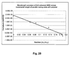
- Fig. 20 is a plot of center wavelength curvature of AWG devices athermalized as described herein, for various ratios of the operative length increment ⁇ L c of the composite waveguide sections to the total physical length increment ⁇ L x of the waveguides. This ratio is referred to herein as the fraction.
- the wavelength curvature (the second order temperature dependency) is largely a linear function of the fraction.
- the wavelength curvature can be minimized by designing the appropriate value for the fraction.
- the value of the fraction can change from embodiment to embodiment. As shown by (eq.
- changes in the operative length increment ⁇ L c of the composite waveguide sections also effect the wavelength slope (the first order temperature dependency).
- the changes in the wavelength slope due to the change in ⁇ L c can be compensated for by adjusting the transversely oriented slots with the slab. This adjustment may include moving the transversely oriented slots up or down along the optical axis in the slab.
- Fig. 21 is a plot of the center wavelength dependency 2100 of an AWG device which has been athermalized as described herein. Also show in Fig. 21 is the measured center wavelength dependency 2105 for a conventional linearly athermalized AWG device.
- the data in Fig. 21 is measured with the AWG input channel connected to a tunable laser and with AWG output channel 21 (of 4) connected to the detector.
- an AWG athermalized as described herein provides an enormous improvement over conventional linearly athermalized devices.
- an AWG device athermalized to the second order as described herein can achieve either a much larger temperature range, or much more densely packed channels, or both, than can a conventional device.
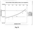
- Fig. 22 is a plot of the measured index-curvature versus the polymer index at room temperature, showing that the index-curvature is different for different compensation materials.
- a polymer with an index above 1.42 at room temperature results in a strong increase in the index curvature.
- the high curvature would allow for athermalization with a smaller operative length increment ⁇ L c of the composite waveguide sections.
- the generally parallel elongated slots described herein demonstrate how one can change the variation of index-curvature with temperature to provide excellent athermalization.
- Generally parallel elongated slots may also or alternatively be implemented to change the variation of the net index of the waveguide with wavelength. This could be of relevance for cyclic AWGs where one wants to control the free spectral range (FSR).
- FSR free spectral range
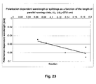
- Another application on the use of generally parallel elongated slots in an AWG is to eliminate, or otherwise control, polarization dependent wavelength. Further applications include to change the variation of birefringence with temperature.
- Fig. 23 is a plot of measured data showing the variation in the polarization of an AWG as a function of the operative length increment ⁇ L c of the composite waveguide sections.
- This change in polarization dependent wavelength originates from a change of the light modification as well as a change of the stress in the cross-section of the composite waveguide sections.
- an AWG is constructed in the same manner as shown in Fig. 7 , but the composite waveguide sections 740 are designed to satisfy all Q of the requirements of (eq. 31).
- the above second order athermalization techniques can be further extended to take into account the temperature dependencies not only of the effective indices of refraction, but also the ⁇ L's.
- ⁇ L c is much smaller than ⁇ L r in a typical embodiment, the mechanical expansion term can be lumped into n 1r without much loss of accuracy.
- n 1r is determined empirically, than the value of n 1r will inherently include contributions from the mechanical expansion term.
- the empirical determination is made using data taken from a chip already packaged in the same manner as would the final product, so that if the packaging of the final product will influence the mechanical expansion exhibited by the chip, those influences are present also in the chip as tested.
- the empirical determination can be made using data taken from an unpackaged chip, and a compliant layer separates the chip from the packaging in the final product.
- athermality can be optimized by using the equations and techniques described herein, it will be possible that an embodiment can still make great improvements in athermality over conventional methods if the equations described herein are only substantially equal to zero, or with a small spoiling factor.
- the phrase "substantially equal to zero" is intended to accommodate manufacturing tolerances. It is also intended to accommodate implementations where the result is a small number that yields an AWG having much better athermality than possible using conventional methods. It is not essential that the equations exactly zero to obtain the benefits of the invention.
Landscapes
- Physics & Mathematics (AREA)
- Engineering & Computer Science (AREA)
- Microelectronics & Electronic Packaging (AREA)
- General Physics & Mathematics (AREA)
- Optics & Photonics (AREA)
- Optical Integrated Circuits (AREA)
Claims (17)
- Un appareil de guide d'ondes en réseau comprenant une pluralité de guides d'ondes (740) à partir d'une région d'espace libre d'entrée vers une région d'espace libre de sortie, la région d'espace libre d'entrée possédant un port d'entrée (712) et la région d'espace libre de sortie possédant un port de sortie (710), chaque guide d'ondes dans la pluralité (740) comprenant :un matériau de coeur (810) ;un matériau de gaine (800) ; etun matériau de compensation à l'intérieur d'une fente (730) allongé dans une direction parallèle au matériau de coeur (810), la fente étant parallèle à un segment du matériau de coeur, le matériau de compensation possédant un indice de réfraction efficace de dépendance en température qui diffère de celui des matériaux de coeur (810) et de gaine (800),dans lequel le matériau de compensation est sélectionné et la fente est disposée de façon à ce qu'au moins les dérivées de premier et second ordre par rapport à la température d'une longueur d'onde centrale de l'appareil de guide d'ondes en réseau à partir du port d'entrée vers le port de sortie sont sensiblement égales à zéro sur toute la plage de températures de -5°C à +70°C.
- L'appareil de la revendication 1, dans lequel :chaque guide d'ondes dans la pluralité (740) a une longueur de trajet optique respective entre une limite d'entrée de la région d'espace libre d'entrée et une limite de sortie de la région d'espace libre de sortie qui diffère de celle d'un guide d'ondes adjacent dans la pluralité (740) par une différence de longueur de trajet optique efficace respective.
- L'appareil de la revendication 1, dans lequel pour chaque guide d'ondes dans la pluralité (740) :le matériau de coeur a une longueur de trajet physique entre une limite d'entrée de la région d'espace libre d'entrée et une limite de sortie de la région d'espace libre de sortie qui diffère de celle du matériau de coeur d'un guide d'ondes adjacent dans la pluralité par une première différence de longueur de trajet ; etle matériau de compensation a une longueur de trajet opératoire dans la direction parallèle au matériau de coeur et qui diffère de celle du matériau de compensation d'un guide d'ondes adjacent dans la pluralité (740) par une seconde différence de longueur de trajet.
- L'appareil de la revendication 3, dans lequel chaque guide d'ondes dans la pluralité (740) comprend :une première fente sur un premier côté du segment du matériau de coeur (810) et contenant le matériau de compensation ; etune seconde fente sur un second côté du segment du matériau de coeur (810) et contenant le matériau de compensation.
- L'appareil de la revendication 3, dans lequel un rapport de la première différence de longueur de trajet à la seconde différence de longueur de trajet est sensiblement le même pour chaque guide d'ondes dans la pluralité (740).
- L'appareil de la revendication 1, dans lequel la fente pour chaque guide d'ondes dans la pluralité (740) n'est pas adjacente aux fentes de chacun des autres guides d'ondes.
- L'appareil de la revendication 1, dans lequel chaque guide d'ondes dans la pluralité (740) comprend en outre un second matériau de compensation dans une seconde fente allongé dans une direction parallèle au second segment de matériau de coeur, le second matériau de compensation ayant un indice de réfraction efficace de dépendance en température qui diffère de celui des matériaux de coeur (810), de gaine (800) et de compensation.
- L'appareil de la revendication 1, comprenant en outre un second matériau de compensation à l'intérieur d'au moins une de la région d'espace libre d'entrée et de la région d'espace libre de sortie, le second matériau de compensation ayant un indice de réfraction efficace de dépendance en température qui diffère de celui des matériaux de coeur (810), de gaine (800).
- L'appareil de la revendication 8, dans lequel le matériau de compensation et le second matériau de compensation sont les mêmes.
- Un procédé pour la fabrication d'un appareil de guide d'ondes en réseau comprenant la formation d'une pluralité de guides d'ondes (740) à partir d'une région d'espace libre d'entrée vers une région d'espace libre de sortie, la formation de chaque guide d'ondes dans la pluralité (740) comprenant :la formation d'un matériau de coeur (810) ;la formation d'un matériau de gaine (800) ; etla formation d'un matériau de compensation à l'intérieur d'une fente (730) allongé dans une direction parallèle au matériau de coeur (810), la fente étant parallèle à un segment du matériau de coeur, le matériau de compensation affectant un profil de mode optique et possédant un indice de réfraction efficace de dépendance en température qui diffère de celui des matériaux de coeur (810) et de gaine (800),dans lequel le matériau de compensation est sélectionné et la fente est disposée de façon à ce qu'au moins les dérivées de premier et second ordre par rapport à la température d'une longueur d'onde centrale de l'appareil de guide d'ondes en réseau à partir du port d'entrée vers le port de sortie est sensiblement égale à zéro sur toute la plage de températures de -5°C à +70°C.
- Le procédé de la revendication 10, dans lequel pour chaque guide d'ondes dans la pluralité (740) :le matériau de coeur (810) a une longueur de trajet physique entre une limite d'entrée de la région d'espace libre d'entrée et une limite de sortie de la région d'espace libre de sortie qui diffère de celle du matériau de coeur d'un guide d'ondes adjacent dans la pluralité (740) par une première différence de longueur de trajet ; etle matériau de compensation a une longueur de trajet opératoire dans la direction parallèle au matériau de coeur et qui diffère de celle du matériau de compensation d'un guide d'ondes adjacent dans la pluralité (740) par une seconde différence de longueur de trajet.
- Le procédé de la revendication 11, dans lequel la formation de chaque guide d'ondes dans la pluralité (740) comprend :la formation d'une première fente sur un premier côté du segment du matériau de coeur (810) et contenant le matériau de compensation ; etla formation d'une seconde fente sur un second côté du segment du matériau de coeur (810) et contenant le matériau de compensation.
- Le procédé de la revendication 11, dans lequel un rapport de la première différence de longueur de trajet à la seconde différence de longueur de trajet est sensiblement le même pour chaque guide d'ondes dans la pluralité (740).
- Le procédé de la revendication 10, dans lequel la fente pour chaque guide d'ondes dans la pluralité (740) n'est pas adjacente aux fentes de chacun des autres guides d'ondes.
- Le procédé de la revendication 10, dans lequel la formation de chaque guide d'ondes dans la pluralité (740) comprend en outre la formation d'un second matériau de compensation dans une seconde fente allongé dans une direction parallèle au second segment de matériau de coeur (810), le second matériau de compensation ayant un indice de réfraction efficace de dépendance en température qui diffère de celui des matériaux de coeur, de gaine (800) et de compensation.
- Le procédé de la revendication 10, comprenant en outre la formation d'un second matériau de compensation à l'intérieur d'au moins une de la région d'espace libre d'entrée et de la région d'espace libre de sortie, le second matériau de compensation ayant un indice de réfraction efficace de dépendance en température qui diffère de celui des matériaux de coeur (810), de gaine (800).
- L'appareil de la revendication 16, dans lequel le matériau de compensation et le second matériau de compensation sont les mêmes.
Applications Claiming Priority (2)
| Application Number | Priority Date | Filing Date | Title |
|---|---|---|---|
| US31582410P | 2010-03-19 | 2010-03-19 | |
| PCT/US2011/029069 WO2011116333A1 (fr) | 2010-03-19 | 2011-03-18 | Réseau sélectif planaire compensé en température jusqu'au deuxième ordre renfermant des fentes longitudinales |
Publications (2)
| Publication Number | Publication Date |
|---|---|
| EP2548058A1 EP2548058A1 (fr) | 2013-01-23 |
| EP2548058B1 true EP2548058B1 (fr) | 2014-11-19 |
Family
ID=44063486
Family Applications (1)
| Application Number | Title | Priority Date | Filing Date |
|---|---|---|---|
| EP11711225.0A Not-in-force EP2548058B1 (fr) | 2010-03-19 | 2011-03-18 | Réseau de diffraction à guides d'onde compensé en température jusqu'au deuxième ordre comprenant des fentes longitudinales |
Country Status (3)
| Country | Link |
|---|---|
| US (1) | US8873910B2 (fr) |
| EP (1) | EP2548058B1 (fr) |
| WO (1) | WO2011116333A1 (fr) |
Cited By (1)
| Publication number | Priority date | Publication date | Assignee | Title |
|---|---|---|---|---|
| CN109471219A (zh) * | 2018-11-28 | 2019-03-15 | 武汉光迅科技股份有限公司 | 一种awg芯片、制作方法及其调节方法 |
Families Citing this family (15)
| Publication number | Priority date | Publication date | Assignee | Title |
|---|---|---|---|---|
| US20130101252A1 (en) * | 2011-10-19 | 2013-04-25 | Alcatel-Lucent Usa Inc. | Arrayed-waveguide grating having tailored thermal-shift characteristics and an optical assembly employing the same |
| US9722706B1 (en) * | 2013-05-17 | 2017-08-01 | Kaiam Corp. | Multiple wavelength light-source with tracking multiplexer |
| US9482862B2 (en) * | 2013-07-26 | 2016-11-01 | Neophotonics Corporation | Adjustable grid tracking transmitters and receivers |
| US9880352B2 (en) | 2015-07-22 | 2018-01-30 | BB Photonics Inc. | Compound semiconductor photonic integrated circuit with dielectric waveguide |
| US10488589B2 (en) * | 2017-02-08 | 2019-11-26 | Rockley Photonics Limited | T-shaped arrayed waveguide grating |
| US10439720B2 (en) | 2017-05-19 | 2019-10-08 | Adolite Inc. | FPC-based optical interconnect module on glass interposer |
| WO2019016603A1 (fr) * | 2017-07-17 | 2019-01-24 | Rockley Photonics Limited | Filtre d'interférence à trajets multiples athermalisé |
| US10429588B1 (en) * | 2017-10-27 | 2019-10-01 | The Regents Of The University Of California | Chirped grating surface emitter with uniform power emission for beam-steering applications |
| CA3092131C (fr) | 2018-02-22 | 2023-01-17 | Nippon Telegraph And Telephone Corporation | Circuit d'interferometre optique de type guide d'ondes |
| JP7070226B2 (ja) * | 2018-08-09 | 2022-05-18 | 日本電信電話株式会社 | 光導波路デバイスを透過する信号光の透過波長を調整する方法 |
| DE112020001684T5 (de) * | 2019-03-29 | 2022-01-13 | Voyant Photonics, Inc. | Strahlformung durch chipinternen Spiegel |
| CN110376677B (zh) | 2019-08-30 | 2024-10-01 | 深圳铱加科技有限公司 | 一种无热阵列波导光栅 |
| JP7510079B2 (ja) * | 2020-08-03 | 2024-07-03 | 日本電信電話株式会社 | 光回路 |
| CN113448011B (zh) * | 2021-06-29 | 2022-07-05 | 武汉光迅科技股份有限公司 | 一种无热awg的设计方法和装置 |
| US20230019747A1 (en) * | 2022-09-23 | 2023-01-19 | Richard Jones | Hybrid laser architecture with asymmetric metal shunt |
Family Cites Families (48)
| Publication number | Priority date | Publication date | Assignee | Title |
|---|---|---|---|---|
| US5002350A (en) | 1990-02-26 | 1991-03-26 | At&T Bell Laboratories | Optical multiplexer/demultiplexer |
| JP3467534B2 (ja) | 1994-06-28 | 2003-11-17 | オプトゥン (ビーヴィアイ) リミテッド | 光波長チャネルを空間的に分離及び/又は集合する装置 |
| JP3209042B2 (ja) | 1995-06-07 | 2001-09-17 | 日立電線株式会社 | マッハツェンダ光回路 |
| JPH0930251A (ja) | 1995-07-19 | 1997-02-04 | Koa Pack Nishikawa:Kk | 簡易形日除とその製造方法 |
| JPH0943440A (ja) | 1995-07-28 | 1997-02-14 | Toshiba Corp | 集積化光合分波器 |
| US5629992A (en) | 1995-09-14 | 1997-05-13 | Bell Communications Research, Inc. | Passband flattening of integrated optical filters |
| FR2742882B1 (fr) | 1995-12-22 | 1998-02-13 | Corning Inc | Demultiplexeur de longueurs d'onde, realise en optique integree |
| TW355752B (en) | 1996-09-27 | 1999-04-11 | Siemens Ag | Optical coupling-device to couple the light between two waveguide-end-face |
| FR2757722B1 (fr) | 1996-12-23 | 1999-03-19 | France Telecom | Multiplexeur et/ou demultiplexeur optique independant de la temperature |
| JP3436937B2 (ja) | 1997-02-14 | 2003-08-18 | 日本電信電話株式会社 | 光導波回路及び製造方法並びに該光導波回路を有する光導波回路モジュール |
| JPH1144825A (ja) | 1997-07-28 | 1999-02-16 | Fujitsu Ltd | 光デバイス及びその製造方法 |
| US6137939A (en) | 1997-10-01 | 2000-10-24 | Lucent Technologies Inc. | Method and apparatus for reducing temperature-related spectrum shifts in optical devices |
| US5978539A (en) | 1997-10-03 | 1999-11-02 | Lucent Technologies Inc. | Optical device having a temperature independent spectral response using nonplanar geometric distortion of a substrate |
| WO1999021038A1 (fr) | 1997-10-17 | 1999-04-29 | Akzo Nobel N.V. | Multiplexeur de longueurs d'onde a groupement a dephasage |
| US6169838B1 (en) | 1998-04-17 | 2001-01-02 | Jian-Jun He | Athermal waveguide grating based device having a temperature compensator in the slab waveguide region |
| US5937113A (en) | 1998-04-17 | 1999-08-10 | National Research Council Of Canada | Optical grating-based device having a slab waveguide polarization compensating region |
| GB9813281D0 (en) | 1998-06-19 | 1998-08-19 | Bookham Technology Ltd | Temperature stable integrated optical device |
| DE19934185A1 (de) | 1999-07-21 | 2001-01-25 | Siemens Ag | Optische Kopplungseinrichtung |
| DE19934183A1 (de) | 1999-07-21 | 2001-01-25 | Siemens Ag | Optische Kopplungseinrichtung |
| DE19934179A1 (de) | 1999-07-21 | 2001-01-25 | Siemens Ag | Optische Kopplungseinrichtung |
| DE19934178A1 (de) | 1999-07-21 | 2001-01-25 | Siemens Ag | Optische Kopplungseinrichtung |
| DE19934184A1 (de) | 1999-07-21 | 2001-01-25 | Siemens Ag | Optische Kopplungseinrichtung |
| JP2001051138A (ja) | 1999-08-10 | 2001-02-23 | Hitachi Cable Ltd | 温度無依存性光合分波器 |
| EP1089098B1 (fr) | 1999-09-28 | 2008-02-13 | Corning Incorporated | Multiplexeur à réseau de guides d'onde (AWG) athermique avec segment de polymère, et procédé de fabrication |
| US6289147B1 (en) | 1999-11-01 | 2001-09-11 | Bbv Design Bv | Passband flattening of a phasar |
| EP1116973A1 (fr) | 2000-01-11 | 2001-07-18 | Corning Incorporated | Dispositifs à guides d'onde optique intégrés athermalisés |
| US6757454B2 (en) | 2000-02-10 | 2004-06-29 | Nippon Telegraph And Telephone Corporation | Polarization desensitized optical waveguide interferometer |
| JP2001255423A (ja) | 2000-03-13 | 2001-09-21 | Furukawa Electric Co Ltd:The | 光部品 |
| US6985656B2 (en) | 2000-03-16 | 2006-01-10 | Lightsmyth Technologies Inc | Temperature-compensated planar waveguide optical apparatus |
| GB2370128A (en) | 2000-12-12 | 2002-06-19 | Kymata Ltd | Arrayed waveguide grating with optical delay regions |
| JP3764105B2 (ja) | 2001-03-13 | 2006-04-05 | 古河電気工業株式会社 | アレイ導波路回折格子型光合分波器 |
| US6735364B2 (en) | 2001-08-27 | 2004-05-11 | The Furukawa Electric Co., Ltd. | Arrayed waveguide grating optical multiplexer/demultiplexer and method for manufacturing the same |
| US20030039008A1 (en) | 2001-08-27 | 2003-02-27 | Michael Davies | Optical grating for coarse wavelength division multiplexing (CWDM) applications |
| GB2379517B (en) | 2001-09-11 | 2003-08-13 | Kymata Netherlands B V | Optical arrayed waveguide grating |
| US7130517B2 (en) | 2001-09-14 | 2006-10-31 | Photon X, Llc | Athermal polymer optical waveguide on polymer substrate |
| JP2003121666A (ja) | 2001-10-10 | 2003-04-23 | Nec Corp | 導波路型光デバイスおよびその製造方法 |
| AU2002353969A1 (en) | 2001-11-01 | 2003-05-12 | Massachusetts Institute Of Technology | Arrayed waveguide grating |
| EP1319967A1 (fr) | 2001-12-13 | 2003-06-18 | Alcatel | Réseau de guides d'ondes optiques athermique avec compensation thermique dans la zone du guide planaire |
| US6697553B2 (en) | 2002-02-15 | 2004-02-24 | Jds Uniphase Corporation | Compact, low insertion loss, high yield arrayed waveguide grating |
| US7194162B2 (en) | 2002-02-22 | 2007-03-20 | Neophotonics Corporation | Filter response optimization for an arrayed waveguide grating device by adjusting grating optical path length at nanometer scale |
| JP3404031B2 (ja) | 2002-03-25 | 2003-05-06 | 株式会社東芝 | 集積化光合分波器 |
| EP1367418A1 (fr) | 2002-05-30 | 2003-12-03 | Alcatel | Réseau de guides d'ondes athermique |
| US7177499B2 (en) | 2003-03-28 | 2007-02-13 | Intel Corporation | Athermal package for fiber bragg gratings with compensation for non-linear thermal response |
| US7013065B2 (en) | 2003-10-22 | 2006-03-14 | Klaus Petermann | Planar optical apparatus for setting the chromatic dispersion in an optical system |
| US7187818B2 (en) | 2004-01-16 | 2007-03-06 | Her Majesty The Queen In Right Of Canada, As Represented By The Minister Of Industry, Through The Communications Research Centre Canada | Packaging for planar lightwave circuits |
| KR100763790B1 (ko) | 2005-01-07 | 2007-10-08 | (주)포인테크 | 온도 무의존성 광도파로열 격자 및 그 제작방법 |
| US7397986B2 (en) | 2005-03-04 | 2008-07-08 | Gemfire Corporation | Optical device with reduced temperature dependence |
| EP2253976B1 (fr) | 2008-02-22 | 2015-10-07 | NTT Electronics Corporation | Dispositif optique de type guide d'ondes |
-
2011
- 2011-03-18 EP EP11711225.0A patent/EP2548058B1/fr not_active Not-in-force
- 2011-03-18 US US13/051,900 patent/US8873910B2/en not_active Expired - Fee Related
- 2011-03-18 WO PCT/US2011/029069 patent/WO2011116333A1/fr not_active Ceased
Cited By (1)
| Publication number | Priority date | Publication date | Assignee | Title |
|---|---|---|---|---|
| CN109471219A (zh) * | 2018-11-28 | 2019-03-15 | 武汉光迅科技股份有限公司 | 一种awg芯片、制作方法及其调节方法 |
Also Published As
| Publication number | Publication date |
|---|---|
| US20110229080A1 (en) | 2011-09-22 |
| WO2011116333A1 (fr) | 2011-09-22 |
| EP2548058A1 (fr) | 2013-01-23 |
| US8873910B2 (en) | 2014-10-28 |
Similar Documents
| Publication | Publication Date | Title |
|---|---|---|
| US8873910B2 (en) | Optical device with athermal slots for temperature dependence curvature reduction | |
| US7397986B2 (en) | Optical device with reduced temperature dependence | |
| US6757454B2 (en) | Polarization desensitized optical waveguide interferometer | |
| CN102099718B (zh) | 光波长合分波回路 | |
| US6169838B1 (en) | Athermal waveguide grating based device having a temperature compensator in the slab waveguide region | |
| CA2315458C (fr) | Multiplexeur/demultiplexeur optique | |
| US20020181868A1 (en) | Arrayed waveguide grating with waveguides of unequal widths | |
| JP4385224B2 (ja) | 光導波路デバイス及び光導波路モジュール | |
| CN110573918B (zh) | T形阵列式波导光栅 | |
| US20020181857A1 (en) | Optical wavelength multiplexer/demultiplexer | |
| EP2253976B1 (fr) | Dispositif optique de type guide d'ondes | |
| EP1319967A1 (fr) | Réseau de guides d'ondes optiques athermique avec compensation thermique dans la zone du guide planaire | |
| Buchold et al. | Polarisation insensitive arrayed-waveguide grating multiplexers with ion-exchanged waveguides in glass | |
| JP2011158730A (ja) | 温度無依存光回路 | |
| WO2004001470A1 (fr) | Reseau selectif planaire athermique | |
| US7072546B2 (en) | Compensation for chromatic dispersion | |
| Pandraud et al. | Technique for widening passband of wavelength router |
Legal Events
| Date | Code | Title | Description |
|---|---|---|---|
| PUAI | Public reference made under article 153(3) epc to a published international application that has entered the european phase |
Free format text: ORIGINAL CODE: 0009012 |
|
| 17P | Request for examination filed |
Effective date: 20121015 |
|
| AK | Designated contracting states |
Kind code of ref document: A1 Designated state(s): AL AT BE BG CH CY CZ DE DK EE ES FI FR GB GR HR HU IE IS IT LI LT LU LV MC MK MT NL NO PL PT RO RS SE SI SK SM TR |
|
| DAX | Request for extension of the european patent (deleted) | ||
| 17Q | First examination report despatched |
Effective date: 20130916 |
|
| GRAP | Despatch of communication of intention to grant a patent |
Free format text: ORIGINAL CODE: EPIDOSNIGR1 |
|
| INTG | Intention to grant announced |
Effective date: 20140718 |
|
| GRAS | Grant fee paid |
Free format text: ORIGINAL CODE: EPIDOSNIGR3 |
|
| GRAA | (expected) grant |
Free format text: ORIGINAL CODE: 0009210 |
|
| RAP1 | Party data changed (applicant data changed or rights of an application transferred) |
Owner name: GEMFIRE CORPORATION |
|
| AK | Designated contracting states |
Kind code of ref document: B1 Designated state(s): AL AT BE BG CH CY CZ DE DK EE ES FI FR GB GR HR HU IE IS IT LI LT LU LV MC MK MT NL NO PL PT RO RS SE SI SK SM TR |
|
| REG | Reference to a national code |
Ref country code: GB Ref legal event code: FG4D |
|
| REG | Reference to a national code |
Ref country code: CH Ref legal event code: EP |
|
| REG | Reference to a national code |
Ref country code: AT Ref legal event code: REF Ref document number: 697330 Country of ref document: AT Kind code of ref document: T Effective date: 20141215 |
|
| REG | Reference to a national code |
Ref country code: IE Ref legal event code: FG4D |
|
| REG | Reference to a national code |
Ref country code: DE Ref legal event code: R096 Ref document number: 602011011503 Country of ref document: DE Effective date: 20141231 |
|
| REG | Reference to a national code |
Ref country code: FR Ref legal event code: PLFP Year of fee payment: 5 |
|
| REG | Reference to a national code |
Ref country code: NL Ref legal event code: VDEP Effective date: 20141119 |
|
| REG | Reference to a national code |
Ref country code: AT Ref legal event code: MK05 Ref document number: 697330 Country of ref document: AT Kind code of ref document: T Effective date: 20141119 |
|
| REG | Reference to a national code |
Ref country code: LT Ref legal event code: MG4D |
|
| PG25 | Lapsed in a contracting state [announced via postgrant information from national office to epo] |
Ref country code: ES Free format text: LAPSE BECAUSE OF FAILURE TO SUBMIT A TRANSLATION OF THE DESCRIPTION OR TO PAY THE FEE WITHIN THE PRESCRIBED TIME-LIMIT Effective date: 20141119 Ref country code: IS Free format text: LAPSE BECAUSE OF FAILURE TO SUBMIT A TRANSLATION OF THE DESCRIPTION OR TO PAY THE FEE WITHIN THE PRESCRIBED TIME-LIMIT Effective date: 20150319 Ref country code: PT Free format text: LAPSE BECAUSE OF FAILURE TO SUBMIT A TRANSLATION OF THE DESCRIPTION OR TO PAY THE FEE WITHIN THE PRESCRIBED TIME-LIMIT Effective date: 20150319 Ref country code: LT Free format text: LAPSE BECAUSE OF FAILURE TO SUBMIT A TRANSLATION OF THE DESCRIPTION OR TO PAY THE FEE WITHIN THE PRESCRIBED TIME-LIMIT Effective date: 20141119 Ref country code: NL Free format text: LAPSE BECAUSE OF FAILURE TO SUBMIT A TRANSLATION OF THE DESCRIPTION OR TO PAY THE FEE WITHIN THE PRESCRIBED TIME-LIMIT Effective date: 20141119 Ref country code: FI Free format text: LAPSE BECAUSE OF FAILURE TO SUBMIT A TRANSLATION OF THE DESCRIPTION OR TO PAY THE FEE WITHIN THE PRESCRIBED TIME-LIMIT Effective date: 20141119 Ref country code: NO Free format text: LAPSE BECAUSE OF FAILURE TO SUBMIT A TRANSLATION OF THE DESCRIPTION OR TO PAY THE FEE WITHIN THE PRESCRIBED TIME-LIMIT Effective date: 20150219 |
|
| PG25 | Lapsed in a contracting state [announced via postgrant information from national office to epo] |
Ref country code: LV Free format text: LAPSE BECAUSE OF FAILURE TO SUBMIT A TRANSLATION OF THE DESCRIPTION OR TO PAY THE FEE WITHIN THE PRESCRIBED TIME-LIMIT Effective date: 20141119 Ref country code: AT Free format text: LAPSE BECAUSE OF FAILURE TO SUBMIT A TRANSLATION OF THE DESCRIPTION OR TO PAY THE FEE WITHIN THE PRESCRIBED TIME-LIMIT Effective date: 20141119 Ref country code: GR Free format text: LAPSE BECAUSE OF FAILURE TO SUBMIT A TRANSLATION OF THE DESCRIPTION OR TO PAY THE FEE WITHIN THE PRESCRIBED TIME-LIMIT Effective date: 20150220 Ref country code: PL Free format text: LAPSE BECAUSE OF FAILURE TO SUBMIT A TRANSLATION OF THE DESCRIPTION OR TO PAY THE FEE WITHIN THE PRESCRIBED TIME-LIMIT Effective date: 20141119 Ref country code: HR Free format text: LAPSE BECAUSE OF FAILURE TO SUBMIT A TRANSLATION OF THE DESCRIPTION OR TO PAY THE FEE WITHIN THE PRESCRIBED TIME-LIMIT Effective date: 20141119 Ref country code: SE Free format text: LAPSE BECAUSE OF FAILURE TO SUBMIT A TRANSLATION OF THE DESCRIPTION OR TO PAY THE FEE WITHIN THE PRESCRIBED TIME-LIMIT Effective date: 20141119 Ref country code: RS Free format text: LAPSE BECAUSE OF FAILURE TO SUBMIT A TRANSLATION OF THE DESCRIPTION OR TO PAY THE FEE WITHIN THE PRESCRIBED TIME-LIMIT Effective date: 20141119 Ref country code: CY Free format text: LAPSE BECAUSE OF FAILURE TO SUBMIT A TRANSLATION OF THE DESCRIPTION OR TO PAY THE FEE WITHIN THE PRESCRIBED TIME-LIMIT Effective date: 20141119 |
|
| PGFP | Annual fee paid to national office [announced via postgrant information from national office to epo] |
Ref country code: FR Payment date: 20150317 Year of fee payment: 5 |
|
| PG25 | Lapsed in a contracting state [announced via postgrant information from national office to epo] |
Ref country code: SK Free format text: LAPSE BECAUSE OF FAILURE TO SUBMIT A TRANSLATION OF THE DESCRIPTION OR TO PAY THE FEE WITHIN THE PRESCRIBED TIME-LIMIT Effective date: 20141119 Ref country code: RO Free format text: LAPSE BECAUSE OF FAILURE TO SUBMIT A TRANSLATION OF THE DESCRIPTION OR TO PAY THE FEE WITHIN THE PRESCRIBED TIME-LIMIT Effective date: 20141119 Ref country code: DK Free format text: LAPSE BECAUSE OF FAILURE TO SUBMIT A TRANSLATION OF THE DESCRIPTION OR TO PAY THE FEE WITHIN THE PRESCRIBED TIME-LIMIT Effective date: 20141119 Ref country code: CZ Free format text: LAPSE BECAUSE OF FAILURE TO SUBMIT A TRANSLATION OF THE DESCRIPTION OR TO PAY THE FEE WITHIN THE PRESCRIBED TIME-LIMIT Effective date: 20141119 Ref country code: EE Free format text: LAPSE BECAUSE OF FAILURE TO SUBMIT A TRANSLATION OF THE DESCRIPTION OR TO PAY THE FEE WITHIN THE PRESCRIBED TIME-LIMIT Effective date: 20141119 |
|
| REG | Reference to a national code |
Ref country code: DE Ref legal event code: R097 Ref document number: 602011011503 Country of ref document: DE |
|
| PLBE | No opposition filed within time limit |
Free format text: ORIGINAL CODE: 0009261 |
|
| STAA | Information on the status of an ep patent application or granted ep patent |
Free format text: STATUS: NO OPPOSITION FILED WITHIN TIME LIMIT |
|
| 26N | No opposition filed |
Effective date: 20150820 |
|
| PG25 | Lapsed in a contracting state [announced via postgrant information from national office to epo] |
Ref country code: LU Free format text: LAPSE BECAUSE OF FAILURE TO SUBMIT A TRANSLATION OF THE DESCRIPTION OR TO PAY THE FEE WITHIN THE PRESCRIBED TIME-LIMIT Effective date: 20150318 Ref country code: MC Free format text: LAPSE BECAUSE OF FAILURE TO SUBMIT A TRANSLATION OF THE DESCRIPTION OR TO PAY THE FEE WITHIN THE PRESCRIBED TIME-LIMIT Effective date: 20141119 |
|
| REG | Reference to a national code |
Ref country code: CH Ref legal event code: PL |
|
| PG25 | Lapsed in a contracting state [announced via postgrant information from national office to epo] |
Ref country code: IT Free format text: LAPSE BECAUSE OF FAILURE TO SUBMIT A TRANSLATION OF THE DESCRIPTION OR TO PAY THE FEE WITHIN THE PRESCRIBED TIME-LIMIT Effective date: 20141119 |
|
| REG | Reference to a national code |
Ref country code: IE Ref legal event code: MM4A |
|
| PG25 | Lapsed in a contracting state [announced via postgrant information from national office to epo] |
Ref country code: LI Free format text: LAPSE BECAUSE OF NON-PAYMENT OF DUE FEES Effective date: 20150331 Ref country code: CH Free format text: LAPSE BECAUSE OF NON-PAYMENT OF DUE FEES Effective date: 20150331 Ref country code: IE Free format text: LAPSE BECAUSE OF NON-PAYMENT OF DUE FEES Effective date: 20150318 |
|
| PG25 | Lapsed in a contracting state [announced via postgrant information from national office to epo] |
Ref country code: SI Free format text: LAPSE BECAUSE OF FAILURE TO SUBMIT A TRANSLATION OF THE DESCRIPTION OR TO PAY THE FEE WITHIN THE PRESCRIBED TIME-LIMIT Effective date: 20141119 |
|
| PG25 | Lapsed in a contracting state [announced via postgrant information from national office to epo] |
Ref country code: MT Free format text: LAPSE BECAUSE OF FAILURE TO SUBMIT A TRANSLATION OF THE DESCRIPTION OR TO PAY THE FEE WITHIN THE PRESCRIBED TIME-LIMIT Effective date: 20141119 |
|
| REG | Reference to a national code |
Ref country code: FR Ref legal event code: ST Effective date: 20161130 |
|
| PG25 | Lapsed in a contracting state [announced via postgrant information from national office to epo] |
Ref country code: FR Free format text: LAPSE BECAUSE OF NON-PAYMENT OF DUE FEES Effective date: 20160331 |
|
| PG25 | Lapsed in a contracting state [announced via postgrant information from national office to epo] |
Ref country code: HU Free format text: LAPSE BECAUSE OF FAILURE TO SUBMIT A TRANSLATION OF THE DESCRIPTION OR TO PAY THE FEE WITHIN THE PRESCRIBED TIME-LIMIT; INVALID AB INITIO Effective date: 20110318 Ref country code: BG Free format text: LAPSE BECAUSE OF FAILURE TO SUBMIT A TRANSLATION OF THE DESCRIPTION OR TO PAY THE FEE WITHIN THE PRESCRIBED TIME-LIMIT Effective date: 20141119 Ref country code: SM Free format text: LAPSE BECAUSE OF FAILURE TO SUBMIT A TRANSLATION OF THE DESCRIPTION OR TO PAY THE FEE WITHIN THE PRESCRIBED TIME-LIMIT Effective date: 20141119 |
|
| PG25 | Lapsed in a contracting state [announced via postgrant information from national office to epo] |
Ref country code: TR Free format text: LAPSE BECAUSE OF FAILURE TO SUBMIT A TRANSLATION OF THE DESCRIPTION OR TO PAY THE FEE WITHIN THE PRESCRIBED TIME-LIMIT Effective date: 20141119 |
|
| PG25 | Lapsed in a contracting state [announced via postgrant information from national office to epo] |
Ref country code: BE Free format text: LAPSE BECAUSE OF FAILURE TO SUBMIT A TRANSLATION OF THE DESCRIPTION OR TO PAY THE FEE WITHIN THE PRESCRIBED TIME-LIMIT Effective date: 20141119 |
|
| PG25 | Lapsed in a contracting state [announced via postgrant information from national office to epo] |
Ref country code: MK Free format text: LAPSE BECAUSE OF FAILURE TO SUBMIT A TRANSLATION OF THE DESCRIPTION OR TO PAY THE FEE WITHIN THE PRESCRIBED TIME-LIMIT Effective date: 20141119 |
|
| PGFP | Annual fee paid to national office [announced via postgrant information from national office to epo] |
Ref country code: DE Payment date: 20180529 Year of fee payment: 8 |
|
| PG25 | Lapsed in a contracting state [announced via postgrant information from national office to epo] |
Ref country code: AL Free format text: LAPSE BECAUSE OF FAILURE TO SUBMIT A TRANSLATION OF THE DESCRIPTION OR TO PAY THE FEE WITHIN THE PRESCRIBED TIME-LIMIT Effective date: 20141119 |
|
| PGFP | Annual fee paid to national office [announced via postgrant information from national office to epo] |
Ref country code: GB Payment date: 20180427 Year of fee payment: 8 |
|
| REG | Reference to a national code |
Ref country code: DE Ref legal event code: R082 Ref document number: 602011011503 Country of ref document: DE Representative=s name: PAGE, WHITE & FARRER GERMANY LLP, DE |
|
| REG | Reference to a national code |
Ref country code: GB Ref legal event code: 732E Free format text: REGISTERED BETWEEN 20190711 AND 20190717 |
|
| REG | Reference to a national code |
Ref country code: DE Ref legal event code: R119 Ref document number: 602011011503 Country of ref document: DE |
|
| GBPC | Gb: european patent ceased through non-payment of renewal fee |
Effective date: 20190318 |
|
| PG25 | Lapsed in a contracting state [announced via postgrant information from national office to epo] |
Ref country code: GB Free format text: LAPSE BECAUSE OF NON-PAYMENT OF DUE FEES Effective date: 20190318 Ref country code: DE Free format text: LAPSE BECAUSE OF NON-PAYMENT OF DUE FEES Effective date: 20191001 |