EP2548076B1 - Dispositif de variation optique, son utilisation et procédé de sa fabrication. - Google Patents
Dispositif de variation optique, son utilisation et procédé de sa fabrication. Download PDFInfo
- Publication number
- EP2548076B1 EP2548076B1 EP11715948.3A EP11715948A EP2548076B1 EP 2548076 B1 EP2548076 B1 EP 2548076B1 EP 11715948 A EP11715948 A EP 11715948A EP 2548076 B1 EP2548076 B1 EP 2548076B1
- Authority
- EP
- European Patent Office
- Prior art keywords
- optical
- optically variable
- electrodes
- electrode
- layer
- Prior art date
- Legal status (The legal status is an assumption and is not a legal conclusion. Google has not performed a legal analysis and makes no representation as to the accuracy of the status listed.)
- Active
Links
Images


Classifications
-
- G—PHYSICS
- G02—OPTICS
- G02F—OPTICAL DEVICES OR ARRANGEMENTS FOR THE CONTROL OF LIGHT BY MODIFICATION OF THE OPTICAL PROPERTIES OF THE MEDIA OF THE ELEMENTS INVOLVED THEREIN; NON-LINEAR OPTICS; FREQUENCY-CHANGING OF LIGHT; OPTICAL LOGIC ELEMENTS; OPTICAL ANALOGUE/DIGITAL CONVERTERS
- G02F1/00—Devices or arrangements for the control of the intensity, colour, phase, polarisation or direction of light arriving from an independent light source, e.g. switching, gating or modulating; Non-linear optics
- G02F1/29—Devices or arrangements for the control of the intensity, colour, phase, polarisation or direction of light arriving from an independent light source, e.g. switching, gating or modulating; Non-linear optics for the control of the position or the direction of light beams, i.e. deflection
-
- G—PHYSICS
- G02—OPTICS
- G02F—OPTICAL DEVICES OR ARRANGEMENTS FOR THE CONTROL OF LIGHT BY MODIFICATION OF THE OPTICAL PROPERTIES OF THE MEDIA OF THE ELEMENTS INVOLVED THEREIN; NON-LINEAR OPTICS; FREQUENCY-CHANGING OF LIGHT; OPTICAL LOGIC ELEMENTS; OPTICAL ANALOGUE/DIGITAL CONVERTERS
- G02F1/00—Devices or arrangements for the control of the intensity, colour, phase, polarisation or direction of light arriving from an independent light source, e.g. switching, gating or modulating; Non-linear optics
- G02F1/29—Devices or arrangements for the control of the intensity, colour, phase, polarisation or direction of light arriving from an independent light source, e.g. switching, gating or modulating; Non-linear optics for the control of the position or the direction of light beams, i.e. deflection
- G02F1/292—Devices or arrangements for the control of the intensity, colour, phase, polarisation or direction of light arriving from an independent light source, e.g. switching, gating or modulating; Non-linear optics for the control of the position or the direction of light beams, i.e. deflection by controlled diffraction or phased-array beam steering
-
- G—PHYSICS
- G02—OPTICS
- G02B—OPTICAL ELEMENTS, SYSTEMS OR APPARATUS
- G02B30/00—Optical systems or apparatus for producing three-dimensional [3D] effects, e.g. stereoscopic images
-
- G—PHYSICS
- G02—OPTICS
- G02F—OPTICAL DEVICES OR ARRANGEMENTS FOR THE CONTROL OF LIGHT BY MODIFICATION OF THE OPTICAL PROPERTIES OF THE MEDIA OF THE ELEMENTS INVOLVED THEREIN; NON-LINEAR OPTICS; FREQUENCY-CHANGING OF LIGHT; OPTICAL LOGIC ELEMENTS; OPTICAL ANALOGUE/DIGITAL CONVERTERS
- G02F1/00—Devices or arrangements for the control of the intensity, colour, phase, polarisation or direction of light arriving from an independent light source, e.g. switching, gating or modulating; Non-linear optics
- G02F1/01—Devices or arrangements for the control of the intensity, colour, phase, polarisation or direction of light arriving from an independent light source, e.g. switching, gating or modulating; Non-linear optics for the control of the intensity, phase, polarisation or colour
- G02F1/13—Devices or arrangements for the control of the intensity, colour, phase, polarisation or direction of light arriving from an independent light source, e.g. switching, gating or modulating; Non-linear optics for the control of the intensity, phase, polarisation or colour based on liquid crystals, e.g. single liquid crystal display cells
- G02F1/133—Constructional arrangements; Operation of liquid crystal cells; Circuit arrangements
- G02F1/1333—Constructional arrangements; Manufacturing methods
- G02F1/1343—Electrodes
- G02F1/13439—Electrodes characterised by their electrical, optical, physical properties; materials therefor; method of making
-
- G—PHYSICS
- G02—OPTICS
- G02F—OPTICAL DEVICES OR ARRANGEMENTS FOR THE CONTROL OF LIGHT BY MODIFICATION OF THE OPTICAL PROPERTIES OF THE MEDIA OF THE ELEMENTS INVOLVED THEREIN; NON-LINEAR OPTICS; FREQUENCY-CHANGING OF LIGHT; OPTICAL LOGIC ELEMENTS; OPTICAL ANALOGUE/DIGITAL CONVERTERS
- G02F2201/00—Constructional arrangements not provided for in groups G02F1/00 - G02F7/00
- G02F2201/12—Constructional arrangements not provided for in groups G02F1/00 - G02F7/00 electrode
-
- G—PHYSICS
- G02—OPTICS
- G02F—OPTICAL DEVICES OR ARRANGEMENTS FOR THE CONTROL OF LIGHT BY MODIFICATION OF THE OPTICAL PROPERTIES OF THE MEDIA OF THE ELEMENTS INVOLVED THEREIN; NON-LINEAR OPTICS; FREQUENCY-CHANGING OF LIGHT; OPTICAL LOGIC ELEMENTS; OPTICAL ANALOGUE/DIGITAL CONVERTERS
- G02F2202/00—Materials and properties
- G02F2202/02—Materials and properties organic material
- G02F2202/022—Materials and properties organic material polymeric
-
- G—PHYSICS
- G02—OPTICS
- G02F—OPTICAL DEVICES OR ARRANGEMENTS FOR THE CONTROL OF LIGHT BY MODIFICATION OF THE OPTICAL PROPERTIES OF THE MEDIA OF THE ELEMENTS INVOLVED THEREIN; NON-LINEAR OPTICS; FREQUENCY-CHANGING OF LIGHT; OPTICAL LOGIC ELEMENTS; OPTICAL ANALOGUE/DIGITAL CONVERTERS
- G02F2203/00—Function characteristic
- G02F2203/18—Function characteristic adaptive optics, e.g. wavefront correction
Definitions
- the present invention relates to optical variation devices for controlling the propagation of light and improving the optical qualities of an image viewed by an apparatus comprising such a device.
- optical variation device as defined in claim 1 and illustrated on the Figures 13 to 15 .
- This type of lens offers the advantage of having a variable focal length that is quickly controllable by simple electrical means by applying a voltage signal to the electrodes, the signal may have different frequencies.
- a convergent lens is obtained whose focusing is performed on a point of the optical axis.
- this type of lens has a possibility of variation of the focal length along the optical axis, depending on the frequency and control voltage but it does not provide a three-dimensional control of the focal point to shift the orientation of the optical beam and thus d improve the range of angular scanning of the device.
- the object of the present invention is to overcome these disadvantages, to provide an optical variation device for varying the optical phase so as to improve the optical qualities of the image.
- optical variation device as described above is characterized by the provisions defined in the characterizing part of claim 1; the preamble of this claim is disclosed in the article " Low aberrations symmetrical adaptive modal liquid crystal lens with short focal lengths "by N. Fraval et al., Applied Optics, 49, number 15, pages 2778-2783 .
- the invention offers the possibility of unbalancing the electric field between the electrodes and thus to shift the orientation of the optical beam.
- signals having different voltages and frequencies can be applied to generate more complex electrical surface area profiles that result in asymmetric and complex wavefront shapes.
- the present invention can also be used as an aberration correction solution or conversely, generating deformation of the wavefront depending on the intended application and the desired effects.
- the device is adapted to be used for optical opening lenses of very small diameters, especially less than 2 mm.
- the invention also relates to an optical assembly comprising two optical variation devices stacked one on the other so that their anchoring directions are perpendicular.
- the present invention finds application in the field of imaging so as to better control the optical quality of an image to be viewed with a device equipped with the device according to the invention.
- the optical dimming device 10 is a lens having a liquid crystal element 312 having optical properties controlling the propagation of light.
- the liquid crystal element 312 consists of a liquid crystal, for example nematic having molecules which are initially oriented around the same mean direction. These molecules exhibit anisotropy of the dielectric permittivity and a positive or negative birefringence. The molecules therefore have an ability to orient respectively parallel or perpendicular to the electric field E applied to them. Liquid crystal 312 modifies the polarization of light.
- the optical variation device further comprises two transparent substrates 314, 316 (for example glass, plastics, quartz, etc.). Each substrate is covered with an opaque or transparent metallic layer (Cr, Al, Au ...) or semiconductor (ITO ...) forming a control electrode, which defines substantially at its center a circular opening called optical opening 322, which has a center. A layer of a transparent resistive material 326, 328 is applied in the optical aperture of each electrode so as to fill the latter.
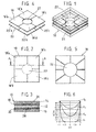
- the figure 3 illustrates a sectional view of a device useful for understanding the invention, which shows the various elements constituting the device 10.
- This frequency-controllable electrical potential distribution makes it possible to generate a variable electric field gradient E in the liquid crystal 12.
- the distribution of the electric field E causes an orientation gradient of the molecules of the liquid crystal 12.
- the liquid crystal 12 thus oriented is considered by polarized light parallel to the long axis of the molecules as a gradient gradient medium.
- the lens 10 formed by the device thus has controllable focusing properties.
- the material layer 26, 28 has resistivity characteristics as a function of the diameter of the optical aperture between 10k ⁇ / square and 10G ⁇ / square. It is assimilated to a resistive electrode.
- the material 26, 28 has a surface resistance greater than 10 M ⁇ / square and can therefore be used for lenses of very small size, for example in micro-cameras. This material 26, 28 makes it possible to free itself from the constraints of dimensions of the lens and makes it possible to perform imaging with very small pupils. This material 26, 28 can be subjected to high frequency signals, because of its high resistivity.
- the layer of material 26, 28 filling the optical aperture 22, 24 has a surface resistance distributed very uniformly, which generates current conduction properties and distribution of the homogeneous electric potential to obtain a wavefront steady and avoid wavefront deformations due to surface condition.
- the material 26, 28 is adapted to be arranged uniformly in the optical opening 22, 24 to obtain a homogeneous distribution of potential.
- uniform means the ability of the material not to present a discontinuity of distribution of the surface resistance in the volume or the surface that it delimits.
- the uniformity of the surface electrical resistance to obtain the uniform distribution of potential that results from the application of a voltage across the layer implies the conditions following: the initial solution of the material must be homogeneous and the layer obtained after annealing must have a constant thickness.
- the first condition is satisfied by producing a solution with permanent stirring and then filtered with a porosity filter of less than 1 .mu.m in order to guarantee the absence of large aggregates which would greatly increase the local surface resistance.
- the layer must be distributed uniformly over the substrate covered with the electrode. This result can be obtained by the spin-coating spin coating technique and / or by the addition of a solvent such as ethylene glycol which makes it possible to modify the molecular organization of the material and makes it possible to homogenize the deposit on the surface of the substrate.
- the layer of the resistive material 26, 28 makes it possible to control the distribution of the voltage and to obtain an electric field gradient effect in the liquid crystal layer by modulating the frequency.
- the device 10 acts as a low-pass device, in which only the low-frequency signals can pass between the electrodes 18, 20. If the frequencies increase, the voltage will vary between the two electrodes 18, 20, revealing a field gradient. E. The higher the frequency of the signal, the less the voltage propagates towards the center of the cell and the more the electric field gradient E is pronounced between the edges and the center of the pupil, thus making it possible to obtain greater E controllable electric field gradient value range.
- the first and the second electrodes 18, 20 of the device 10 are divided into several parts forming sub-electrodes 18'a, 18'b, 18'c, 18'd and / or 20'a, 20'b, 20'c, 20'd adapted to simultaneously receive different potentials.
- the control electrodes 18, 20 of each substrate 14, 16 may be partitioned into 2, 3, 4, 6 or 8 parts, as visible on the figure 5 . The partitioning is performed so that the axes delimiting the sub-electrodes open on the circumference of the optical aperture and delimit arcs of the circle.
- the axes delimiting the sub-electrodes are such that the electrode is divided into N sub-electrodes and the circumference of the optical aperture is divided into N circular arcs of identical lengths.
- the spacing between each sub-electrode 18 ', 20' is greater than or equal to 1 ⁇ m. This distance is adapted to the resistance of the resistive material and the applied voltages so as not to damage the material locally.
- the space between the electrodes it is possible to eliminate the resistive material in the space between the electrodes, for example by using dry etching techniques, the space between the electrodes then being able to be reduced to a dimension of less than 1 ⁇ m.
- the two electrodes 18, 20 are divided identically and are arranged vis-à-vis so that each sub-electrode 18 'of the first electrode 18 is disposed opposite and is associated with an identical sub-electrode 20' of the second electrode 20.
- the application of electrical signals of variable voltage and frequency, but identical on all the subelectrodes 18 ', 20' metal makes it possible to control the position of the focal point along the optical axis, such that the optical function is that of a convergent lens.
- the corresponding phase profile is that of a spherical cap, whose radius of curvature can vary.
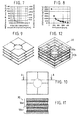
- FIGs 7 and 8 respectively illustrate the curves of the resistance of the material required as a function of the radius of the lens, and the curve of the variation of the focal length as a function of the frequency of the control signals. It can be seen from these figures that for lenses of very small diameters ( ⁇ 0.5 mm) the material must have a high resistance and that lenses of small diameter have a very small focal length. In addition, figure 8 shows that for a very small focal length, the frequency of the signals can be very high (> 400kHz) to obtain a variation of the focal length.
- the lens 10 according to the invention improves image stabilization and can be used, for example as an electro-active element of an imaging lens. It can also be used for laser beam shaping or in any application that requires optical lenses with variable focal lengths.
- the combination of the lenses with variable focal length and beam deflection makes it possible to obtain an autofocus device with miniature angular correction, this association is sought for making micro cameras and adaptive endoscope heads.
- the material 26, 28 in the optical opening may be of transparent conductive polymer type: PEDOT-PSS, polyaniline, polypyrrole ...
- the material 26, 28 disposed between the electrodes 18, 20 is composed of a mixture of poly (-3,4-ethylenedioxythiophene) polystyrene sulfonate and polyvinyl alcohol.
- This material 26, 28 is adapted to be arranged in a uniform layer necessary for the homogeneous distribution of the potential and can be used to produce liquid crystal modal lenses of diameters between 0.5 and 10 mm with low aberrations ( ⁇ / 20) and short focal lengths (1 mm to infinity).
- the device according to the invention is manufactured as follows:
- Each substrate 14, 16 is covered with a metal electrode layer 18, 20 as described above.
- the electrodes 18, 20 are divided into several sub-electrodes 18 ', 20' by conventional etching, for example by photolithography or laser ablation.
- the optical aperture 22, 24 delimited by the electrode 18, 20 receives the layer of material 26, 28 weakly conductive.
- the material consists of a mixture of poly-3,4-ethylenedioxythiophene polystyrenesulfonate (PEDOT-PSS) and polyvinyl alcohol. (PVA).
- the material 26, 28 PEDOT-PSS is deposited on the substrates by a deposition technique known from polymer engineering, such as spin-coating, spraying, or printing.
- the whole is then dried at 100 ° C, for example in an oven.
- shims are, for example, balls of calibrated diameter, for example from 1 to 200 micrometers. They are composed for example of plastic, silica or alumina. According to another method, the calibration of the thickness consists in etching blocks of photosensitive resin.
- the second substrate 16 is then superimposed on the first substrate 14, so that the optical openings 22, 24 of each of the substrates 14, 16 are precisely aligned with each other, and are spaced apart from one another. distance determined by the holds.
- Each sub-electrode 20 'of the second electrode 20 is disposed opposite the sub-electrode 18' corresponding to it of the first electrode 18.
- the assembly is sealed for example by curing the adhesive, either by Ultra violet polymerization or by drying in an oven.
- the liquid crystal element 12 is infiltrated into the cavity formed between the two substrates either by capillarity or vacuum suction. Then a linear polarizer can be positioned at the lens input or output, oriented parallel to the anchoring direction. This polarizer makes it possible to select the light polarization oriented parallel to the anchoring direction.
- the conduction of the PEDOT-PSS layer can be increased by adding a surface resistance promoter to the PEDOT-PSS solution.
- This promoter is, for example, ethylene glycol (EG), dimethyl formamide (DMF).
- PVA makes it possible to reduce and standardize the surface resistance of the deposited material, thus allowing an even more homogeneous distribution of the potential in the material.
- Adhesion of PEDOT-PSS to substrates can be enhanced by adding an adhesion promoter such as tetraethoxysilane.
- planar anchoring treatment can be performed on the material, if the latter supports such treatment.
- the treatment consists of a mechanical action (for example, brushing the surface) which aligns the molecules of the liquid crystal parallel to each other.
- the PEDOT-PSS layers are then brushed with a nylon-coated roller to achieve a planar anchorage of the liquid crystal, that is to say parallel to the substrates.
- Anchoring treatments can be carried out by other methods, for example by depositing a another layer of photo-alignable polymer.
- liquid crystal used has a negative birefringence, it is necessary to achieve a suitable deposition of material so that the anchoring of the liquid crystal is homeotropic, that is to say perpendicular to the substrates, for example silanes.
- the device comprises an anchoring layer, that is to say a layer of another material that supports the anchoring treatment (Poliymide, PVA 7) is deposited on the resistive electrode and a treatment of anchoring is performed so as to constrain the liquid crystal to a planar or homeotropic position.
- an anchoring layer that is to say a layer of another material that supports the anchoring treatment (Poliymide, PVA 7) is deposited on the resistive electrode and a treatment of anchoring is performed so as to constrain the liquid crystal to a planar or homeotropic position.
- the manufacturing techniques outlined above are easily industrializable. All stages are "wafer level", that is to say that they are manufacturing techniques dedicated to microelectronics.
- the "wafer” is a silicon or glass disk on which photolithography is etched respectively into electronic components (transistor, resistors, etc.) or optoelectronic (miniature lenses, OLED, etc.). This makes it possible to highly parallelize the processes and thus to gain profitability.
- These manufacturing techniques can be used and adapted to massively parallel production systems.
- the birefringence ie its property of producing a double refraction of the light
- the birefringence can be negative or positive.
- the application of electrical signals of variable voltage and frequency, but identical on all the sub-electrodes 18 ', 20' makes it possible to control the position of the focal point along the optical axis such that the optical function is that of a divergent lens.
- the invention also relates to an optical assembly 30 consisting of several optical variation devices 10a, 10b assembled to one another.
- the stacked lenses are convergent and their anchoring directions, that is to say their direction of orientation of the liquid crystal, are perpendicular to one another.
- the assembly thus formed becomes a polarized lens that is insensitive to polarization.
- the polarizer must be removed.
- the space between the two devices must be much smaller than the minimum focal length.
- the assembly thus formed becomes two lenses with variable focal lengths.
- the assembly thus formed becomes two lenses with variable focal length, a different focal length per lens, but acting on the same polarization. Only one polarizer is needed for both lenses.
- the assembly in the case where the assembly comprises a convergent lens associated with a diverging lens in an imaging lens, the assembly acquires the properties of a miniature zoom.
- the optical variation devices can be controlled simultaneously, that is to say that the phase, the amplitude and the frequency of the signals applied to each device are equal.
- the devices are controlled independently, that is to say that the phase, the amplitude and the frequency of the signals applied to each device are independent.
- the structure of the optical variation device according to the invention, used in the previous embodiments, is illustrated by the Figures 13 to 15 the resistive pupil, formed by the optical aperture 322, is delimited by a resistive ring (34, 36).
- the resistive ring (34, 36) is controlled by thin metal sub-electrodes (318a, 318b, 318c, 318d, 320a, 320b, 320c, 320d).
- Each sub-electrode (318a to 318d, 320a to 320d) has the shape of a rod connected on the one hand to the resistive ring (34, 36) so as to delimit between them arcs of the ring resistive ring (34, 36) of substantially the same length.
- the optical variation device comprises four sub-electrodes delimiting, on the one hand, four substantially equal arcs of circle and opening on the other hand on the same edge of the substrate plate on which the sub-electrodes are arranged.
- the resistive ring (34, 36) serves to standardize the distribution of the electrical potential on the surface of the layer of material (326, 328) disposed in the optical aperture.
- the resistive ring (34, 36) makes it possible to linearize the electrical voltage between each thin metal electrode (318a to 318d, 320a to 320d). It improves the electrical continuity between the sub-electrodes (318a to 318d, 320a to 320d) while ensuring electrical propagation on each arc of the resistive ring, between the sub-electrodes.
- the optical variation device ensures the conduction of the electric potential in the sub-electrodes (318a to 318d, 320a to 320d), a linear distribution of potential in the resistive ring (34, 36) and therefore a homogeneous distribution of the potential in the pupil. In addition, it allows the modification of the distribution of the electrical potential in the pupil by modifying the control frequency.
- the optical variation device has thin metal sub-electrodes of virtually zero resistance, if the ring has a surface resistance of between 1 and 10 k ⁇ / square, the resistance of the pupil having a surface resistance of 1 ⁇ m. order of several M ⁇ / square.
- the layer of material (326, 328) used in the pupil can be of transparent conductive type: PEDOT-PSS, polyaniline, polypyrrolle, etc.
- the material does not have to be transparent because it delimits the opening optical.
- an optical variation device 410 comprises on each substrate plate 414, 416 an electrode 418, 420 divided into two sub-electrodes 418a, 418b, 420a, 420b rectilinear and arranged in parallel.
- the sub-electrodes of the same substrate plate 414, 416 delimit an optical opening 422, 424 of substantially rectangular shape defining a cylindrical lens.
- the sub-electrodes 418a, 418b, 420a, 420b are adapted to simultaneously receive different potentials. This configuration makes it possible to associate a cylindrical lens function with variable focal length with a variable angle prism function.
- the application of electrical signals of variable voltage and frequency, but identical on all the metal sub-electrodes 418a, 418b, 420a, 420b of the same substrate 414, 416 makes it possible to control the position of the focal line along the optical axis, such that the optical function is that of a convergent cylindrical lens.
- the corresponding phase profile is that of a cylindrical cap or vault, whose radius of curvature may vary.
- An optical assembly comprising devices according to the example of Figures 16 to 18 illustrated by the figures 19 and 20 .
- this optical assembly there are several optical variation devices 410 so that the rectangular optical openings 422, 424 can be made in a network.
- the optical function thus produced is an adjustable lenticular array.
- Each element of the network can be controlled by a control means individually or globally identically to the neighbors.
- a variable lenticular array may be combined with a conventional liquid crystal display 438 to provide an autostereoscopic display function (i.e. a projection rendering a three-dimensional relief print, without the need for glasses), switchable (to switch from a simple 2D display to a 3D display), and to be able to add an adaptation function of the 3D display to the position of the observer.
- an autostereoscopic display function i.e. a projection rendering a three-dimensional relief print, without the need for glasses
- switchable to switch from a simple 2D display to a 3D display
- an adaptation function of the 3D display to the position of the observer.
- the known autostereoscopic 3D displays using the principle of the paralax barrier mask or the principle of the lenticular network do not make it possible to follow the observer, the screen must be viewed at a fixed distance, and at a fixed angle with respect to the 'screen.
- An array of cylindrical lenses according to the example will make it possible to adapt the 3D display to the position of the observer, provided to detect its position defined by the distance d1, d2 and the angular position ( ⁇ 1, ⁇ 1, ⁇ 2, ⁇ 2 ) of the observer with respect to the screen 438 by a specific detection means known to those skilled in the art.
- Device control means is provided for applying electrical signals of voltages and frequencies adapted to change the focal length and prism function of the optical variation devices 410 so as to adjust the direction of the light beam to the observer.
Landscapes
- Physics & Mathematics (AREA)
- Nonlinear Science (AREA)
- General Physics & Mathematics (AREA)
- Optics & Photonics (AREA)
- Mathematical Physics (AREA)
- Chemical & Material Sciences (AREA)
- Crystallography & Structural Chemistry (AREA)
- Liquid Crystal (AREA)
Applications Claiming Priority (2)
| Application Number | Priority Date | Filing Date | Title |
|---|---|---|---|
| FR1001091A FR2957684B1 (fr) | 2010-03-19 | 2010-03-19 | Dispositif de variation optique, ensemble optique et procede de fabrication d'un tel dispositif |
| PCT/FR2011/050563 WO2011114076A1 (fr) | 2010-03-19 | 2011-03-18 | Dispositif de variation optique. ensemble optique et procédé de fabrication d'un tel dispositif. |
Publications (2)
| Publication Number | Publication Date |
|---|---|
| EP2548076A1 EP2548076A1 (fr) | 2013-01-23 |
| EP2548076B1 true EP2548076B1 (fr) | 2014-05-28 |
Family
ID=42355388
Family Applications (1)
| Application Number | Title | Priority Date | Filing Date |
|---|---|---|---|
| EP11715948.3A Active EP2548076B1 (fr) | 2010-03-19 | 2011-03-18 | Dispositif de variation optique, son utilisation et procédé de sa fabrication. |
Country Status (7)
| Country | Link |
|---|---|
| US (1) | US8896772B2 (da) |
| EP (1) | EP2548076B1 (da) |
| JP (1) | JP5938353B2 (da) |
| KR (1) | KR101855304B1 (da) |
| DK (1) | DK2548076T3 (da) |
| FR (1) | FR2957684B1 (da) |
| WO (1) | WO2011114076A1 (da) |
Families Citing this family (23)
| Publication number | Priority date | Publication date | Assignee | Title |
|---|---|---|---|---|
| US9849657B2 (en) * | 2011-03-15 | 2017-12-26 | Douglas J. McKnight | Liquid crystal devices having reduced electrode-gap visibility |
| KR102002325B1 (ko) * | 2011-12-29 | 2019-07-23 | 주식회사 동진쎄미켐 | 액정 표시 장치의 배면전극 형성용 도전성 조성물 및 이를 사용한 배면전극의 형성 방법 |
| TWI459080B (zh) * | 2012-03-01 | 2014-11-01 | Au Optronics Corp | 立體顯示面板以及屏障面板 |
| ES2727498T3 (es) | 2012-09-30 | 2019-10-16 | Optica Amuka A A Ltd | Lentes con potencia y alineación eléctricamente ajustable |
| US11126040B2 (en) | 2012-09-30 | 2021-09-21 | Optica Amuka (A.A.) Ltd. | Electrically-tunable lenses and lens systems |
| TWI477816B (zh) * | 2012-10-24 | 2015-03-21 | Dayu Optoelectronics Co Ltd | 裸眼式立體顯示裝置及其液晶透鏡 |
| CN103792753A (zh) * | 2012-10-31 | 2014-05-14 | 大昱光电股份有限公司 | 裸眼式立体显示装置及其液晶透镜 |
| CN105103045A (zh) * | 2012-12-18 | 2015-11-25 | 兰斯维克托公司 | 具有高级电场控制能力的液晶光学设备 |
| KR102221553B1 (ko) * | 2014-05-09 | 2021-03-02 | 삼성디스플레이 주식회사 | 3차원 표시 장치 및 이를 위한 액정 렌즈 패널 장치 |
| JP6649901B2 (ja) | 2014-06-05 | 2020-02-19 | オプティカ アムカ(エー.エー.)リミテッド | 動的レンズの制御 |
| FR3028052B1 (fr) | 2014-10-31 | 2017-12-08 | Nexter Systems | Cellule reflechissante a reflectivite modulable |
| US9875705B2 (en) * | 2015-05-13 | 2018-01-23 | Boe Technology Group Co., Ltd. | Display apparatus and method of driving the same |
| ES2904889T3 (es) | 2016-04-17 | 2022-04-06 | Optica Amuka A A Ltd | Lente para gafas que comprende una lente de cristal líquido con accionamiento eléctrico mejorado |
| WO2017216716A1 (en) | 2016-06-16 | 2017-12-21 | Optica Amuka (A.A.) Ltd. | Tunable lenses for spectacles |
| TWI608082B (zh) * | 2016-10-11 | 2017-12-11 | 財團法人工業技術研究院 | 變焦透鏡與其形成方法 |
| US11953764B2 (en) | 2017-07-10 | 2024-04-09 | Optica Amuka (A.A.) Ltd. | Tunable lenses with enhanced performance features |
| US11747619B2 (en) | 2017-07-10 | 2023-09-05 | Optica Amuka (A.A.) Ltd. | Virtual reality and augmented reality systems with dynamic vision correction |
| WO2019077442A1 (en) | 2017-10-16 | 2019-04-25 | Optica Amuka (A.A.) Ltd. | ELECTRICALLY ADJUSTABLE GLASS LENSES THAT CAN BE CONTROLLED BY AN EXTERNAL SYSTEM |
| JP2019200258A (ja) * | 2018-05-15 | 2019-11-21 | 凸版印刷株式会社 | 光偏向装置 |
| CN109752323A (zh) * | 2019-01-24 | 2019-05-14 | 南京奥谱依电子科技有限公司 | 用于波谱寻址测调的fp波谱结构、制备方法和光学显微镜 |
| JP7496142B2 (ja) | 2019-06-02 | 2024-06-06 | オプティカ アムカ(エー.エー.)リミテッド | 近視の治療のための電気的に調整可能な視力補助具 |
| JP7430538B2 (ja) * | 2020-01-24 | 2024-02-13 | 株式会社ジャパンディスプレイ | 光制御装置及び照明装置 |
| WO2022221112A1 (en) * | 2021-04-12 | 2022-10-20 | Corning Research & Development Corporation | Waveguide substrate connection systems and methods |
Family Cites Families (9)
| Publication number | Priority date | Publication date | Assignee | Title |
|---|---|---|---|---|
| FR2650400B1 (fr) * | 1989-07-25 | 1991-10-04 | Thomson Csf | Deflecteur electro-optique a cristal liquide |
| US5493427A (en) * | 1993-05-25 | 1996-02-20 | Sharp Kabushiki Kaisha | Three-dimensional display unit with a variable lens |
| JPH11109304A (ja) * | 1997-09-30 | 1999-04-23 | Advantest Corp | 光結合器 |
| JP5073150B2 (ja) * | 2003-06-30 | 2012-11-14 | 旭硝子株式会社 | 光偏向器および光走査装置 |
| WO2006013901A1 (ja) * | 2004-08-04 | 2006-02-09 | Asahi Glass Company, Limited | 液晶レンズ素子および光ヘッド装置 |
| JP4057597B2 (ja) * | 2004-08-26 | 2008-03-05 | 独立行政法人科学技術振興機構 | 光学素子 |
| KR101689817B1 (ko) | 2008-06-21 | 2017-01-09 | 렌즈벡터 인코퍼레이티드 | 효과적인 전극 구조의 동적 재구성을 사용하는 전자 광학 장치 |
| US7894123B2 (en) * | 2009-02-27 | 2011-02-22 | Raytheon Company | Multilayer light modulator |
| US8134636B2 (en) * | 2009-12-14 | 2012-03-13 | Yi-Shin Lin | Autofocusing optical system using tunable lens system |
-
2010
- 2010-03-19 FR FR1001091A patent/FR2957684B1/fr not_active Expired - Fee Related
-
2011
- 2011-03-18 KR KR1020127027412A patent/KR101855304B1/ko not_active Expired - Fee Related
- 2011-03-18 EP EP11715948.3A patent/EP2548076B1/fr active Active
- 2011-03-18 US US13/582,884 patent/US8896772B2/en active Active
- 2011-03-18 WO PCT/FR2011/050563 patent/WO2011114076A1/fr not_active Ceased
- 2011-03-18 JP JP2012557594A patent/JP5938353B2/ja not_active Expired - Fee Related
- 2011-03-18 DK DK11715948.3T patent/DK2548076T3/da active
Also Published As
| Publication number | Publication date |
|---|---|
| DK2548076T3 (da) | 2014-08-04 |
| US20120327351A1 (en) | 2012-12-27 |
| EP2548076A1 (fr) | 2013-01-23 |
| US8896772B2 (en) | 2014-11-25 |
| KR20130058677A (ko) | 2013-06-04 |
| WO2011114076A1 (fr) | 2011-09-22 |
| KR101855304B1 (ko) | 2018-05-08 |
| JP5938353B2 (ja) | 2016-06-22 |
| FR2957684B1 (fr) | 2012-08-03 |
| JP2013522670A (ja) | 2013-06-13 |
| FR2957684A1 (fr) | 2011-09-23 |
Similar Documents
| Publication | Publication Date | Title |
|---|---|---|
| EP2548076B1 (fr) | Dispositif de variation optique, son utilisation et procédé de sa fabrication. | |
| EP2591324B1 (fr) | Analyseur de front d'ondes a microlentilles a cristal liquide | |
| WO2015091834A1 (fr) | Dispositif optique a variation de focale | |
| EP2929310B1 (fr) | Dispositif de mesure et de controle du front d'onde d'un faisceau lumineux coherent | |
| EP0802439A1 (fr) | Microdispositif optomécanique, et application à un microdéflecteur optomécanique | |
| FR2553907A1 (fr) | Modulateur optique | |
| US8228472B2 (en) | Electrically tunable liquid crystal lens with central electrode | |
| EP3926392A1 (fr) | Dispositif optique et procédé de fabrication | |
| Ouyang et al. | A novel tunable grating fabricated with viscoelastic polymer (PDMS) and conductive polymer (PEDOT) | |
| WO2008046820A1 (fr) | Systeme d'imagerie polarimetrique a matrice de lames d'onde programmables a base de materiau avec un tenseur electro-optique isotrope | |
| Kosugi et al. | Surface-normal electro-optic-polymer modulator with silicon subwavelength grating | |
| EP3571721B1 (fr) | Procédé de réalisation collective de circuits électroniques courbes | |
| FR2780520A1 (fr) | Modulateur d'intensite optique et son procede de fabrication | |
| EP1356344A1 (fr) | Dispositif de controle de polarisation dans une liaison optique | |
| EP4198623B1 (fr) | Dispositif de modulation de phase à cristal liquide | |
| CN106154684A (zh) | 展曲取向液晶透镜 | |
| WO2006003313A1 (fr) | Procede de fabrication d’un bloc optique a circuit optique integre par photopolymerisation localisee d’une matrice organique par absorption a deux photons et bloc optique ainsi obtenu | |
| EP4707908A1 (fr) | Dispositif d'affichage d'une image | |
| Hoeh et al. | Silicon-based, ultra-thin, flexible optically tunable metamaterial-bandpass filter in the thz-regime | |
| EP4098606A1 (fr) | Microsystème électromécanique | |
| FR3119888A1 (fr) | Dispositif pyroelectrique comprenant un substrat a couche superficielle pyroelectrique et procede de realisation | |
| FR3045843A1 (fr) | Systeme d'imagerie optique a lentille deformable par des forces electriques et/ou magnetiques | |
| FR2495805A1 (fr) | Dispositif electro-optique de visualisation a cristal liquide et son procede de fabrication | |
| FR3052913A1 (fr) | Capteur optique comportant un reflecteur optique resonant a multiples couches minces de materiaux dielectriques | |
| EP1456712A2 (fr) | Dispositif de controle de la polarisation d'un signal vehicule sous la forme d'un faisceau lumineux, et application correspondante |
Legal Events
| Date | Code | Title | Description |
|---|---|---|---|
| PUAI | Public reference made under article 153(3) epc to a published international application that has entered the european phase |
Free format text: ORIGINAL CODE: 0009012 |
|
| 17P | Request for examination filed |
Effective date: 20121019 |
|
| AK | Designated contracting states |
Kind code of ref document: A1 Designated state(s): AL AT BE BG CH CY CZ DE DK EE ES FI FR GB GR HR HU IE IS IT LI LT LU LV MC MK MT NL NO PL PT RO RS SE SI SK SM TR |
|
| RIN1 | Information on inventor provided before grant (corrected) |
Inventor name: FRAVAL, NICOLAS Inventor name: BERIER, FREDERIC Inventor name: DE BOUGRENET DE LA TOCNAYE, JEAN LOUIS |
|
| DAX | Request for extension of the european patent (deleted) | ||
| GRAP | Despatch of communication of intention to grant a patent |
Free format text: ORIGINAL CODE: EPIDOSNIGR1 |
|
| INTG | Intention to grant announced |
Effective date: 20131218 |
|
| GRAS | Grant fee paid |
Free format text: ORIGINAL CODE: EPIDOSNIGR3 |
|
| GRAA | (expected) grant |
Free format text: ORIGINAL CODE: 0009210 |
|
| AK | Designated contracting states |
Kind code of ref document: B1 Designated state(s): AL AT BE BG CH CY CZ DE DK EE ES FI FR GB GR HR HU IE IS IT LI LT LU LV MC MK MT NL NO PL PT RO RS SE SI SK SM TR |
|
| REG | Reference to a national code |
Ref country code: GB Ref legal event code: FG4D Free format text: NOT ENGLISH |
|
| REG | Reference to a national code |
Ref country code: CH Ref legal event code: EP |
|
| REG | Reference to a national code |
Ref country code: AT Ref legal event code: REF Ref document number: 670397 Country of ref document: AT Kind code of ref document: T Effective date: 20140615 |
|
| REG | Reference to a national code |
Ref country code: IE Ref legal event code: FG4D Free format text: LANGUAGE OF EP DOCUMENT: FRENCH |
|
| REG | Reference to a national code |
Ref country code: DE Ref legal event code: R096 Ref document number: 602011007306 Country of ref document: DE Effective date: 20140710 |
|
| REG | Reference to a national code |
Ref country code: DK Ref legal event code: T3 Effective date: 20140801 |
|
| REG | Reference to a national code |
Ref country code: NL Ref legal event code: T3 |
|
| REG | Reference to a national code |
Ref country code: SE Ref legal event code: TRGR |
|
| REG | Reference to a national code |
Ref country code: AT Ref legal event code: MK05 Ref document number: 670397 Country of ref document: AT Kind code of ref document: T Effective date: 20140528 |
|
| REG | Reference to a national code |
Ref country code: LT Ref legal event code: MG4D |
|
| PG25 | Lapsed in a contracting state [announced via postgrant information from national office to epo] |
Ref country code: CY Free format text: LAPSE BECAUSE OF FAILURE TO SUBMIT A TRANSLATION OF THE DESCRIPTION OR TO PAY THE FEE WITHIN THE PRESCRIBED TIME-LIMIT Effective date: 20140528 Ref country code: GR Free format text: LAPSE BECAUSE OF FAILURE TO SUBMIT A TRANSLATION OF THE DESCRIPTION OR TO PAY THE FEE WITHIN THE PRESCRIBED TIME-LIMIT Effective date: 20140829 Ref country code: LT Free format text: LAPSE BECAUSE OF FAILURE TO SUBMIT A TRANSLATION OF THE DESCRIPTION OR TO PAY THE FEE WITHIN THE PRESCRIBED TIME-LIMIT Effective date: 20140528 Ref country code: NO Free format text: LAPSE BECAUSE OF FAILURE TO SUBMIT A TRANSLATION OF THE DESCRIPTION OR TO PAY THE FEE WITHIN THE PRESCRIBED TIME-LIMIT Effective date: 20140828 |
|
| PG25 | Lapsed in a contracting state [announced via postgrant information from national office to epo] |
Ref country code: AT Free format text: LAPSE BECAUSE OF FAILURE TO SUBMIT A TRANSLATION OF THE DESCRIPTION OR TO PAY THE FEE WITHIN THE PRESCRIBED TIME-LIMIT Effective date: 20140528 Ref country code: RS Free format text: LAPSE BECAUSE OF FAILURE TO SUBMIT A TRANSLATION OF THE DESCRIPTION OR TO PAY THE FEE WITHIN THE PRESCRIBED TIME-LIMIT Effective date: 20140528 Ref country code: HR Free format text: LAPSE BECAUSE OF FAILURE TO SUBMIT A TRANSLATION OF THE DESCRIPTION OR TO PAY THE FEE WITHIN THE PRESCRIBED TIME-LIMIT Effective date: 20140528 Ref country code: LV Free format text: LAPSE BECAUSE OF FAILURE TO SUBMIT A TRANSLATION OF THE DESCRIPTION OR TO PAY THE FEE WITHIN THE PRESCRIBED TIME-LIMIT Effective date: 20140528 |
|
| PG25 | Lapsed in a contracting state [announced via postgrant information from national office to epo] |
Ref country code: PT Free format text: LAPSE BECAUSE OF FAILURE TO SUBMIT A TRANSLATION OF THE DESCRIPTION OR TO PAY THE FEE WITHIN THE PRESCRIBED TIME-LIMIT Effective date: 20140929 |
|
| PG25 | Lapsed in a contracting state [announced via postgrant information from national office to epo] |
Ref country code: RO Free format text: LAPSE BECAUSE OF FAILURE TO SUBMIT A TRANSLATION OF THE DESCRIPTION OR TO PAY THE FEE WITHIN THE PRESCRIBED TIME-LIMIT Effective date: 20140528 Ref country code: EE Free format text: LAPSE BECAUSE OF FAILURE TO SUBMIT A TRANSLATION OF THE DESCRIPTION OR TO PAY THE FEE WITHIN THE PRESCRIBED TIME-LIMIT Effective date: 20140528 Ref country code: CZ Free format text: LAPSE BECAUSE OF FAILURE TO SUBMIT A TRANSLATION OF THE DESCRIPTION OR TO PAY THE FEE WITHIN THE PRESCRIBED TIME-LIMIT Effective date: 20140528 Ref country code: SK Free format text: LAPSE BECAUSE OF FAILURE TO SUBMIT A TRANSLATION OF THE DESCRIPTION OR TO PAY THE FEE WITHIN THE PRESCRIBED TIME-LIMIT Effective date: 20140528 Ref country code: ES Free format text: LAPSE BECAUSE OF FAILURE TO SUBMIT A TRANSLATION OF THE DESCRIPTION OR TO PAY THE FEE WITHIN THE PRESCRIBED TIME-LIMIT Effective date: 20140528 |
|
| PG25 | Lapsed in a contracting state [announced via postgrant information from national office to epo] |
Ref country code: PL Free format text: LAPSE BECAUSE OF FAILURE TO SUBMIT A TRANSLATION OF THE DESCRIPTION OR TO PAY THE FEE WITHIN THE PRESCRIBED TIME-LIMIT Effective date: 20140528 |
|
| REG | Reference to a national code |
Ref country code: DE Ref legal event code: R097 Ref document number: 602011007306 Country of ref document: DE |
|
| PLBE | No opposition filed within time limit |
Free format text: ORIGINAL CODE: 0009261 |
|
| STAA | Information on the status of an ep patent application or granted ep patent |
Free format text: STATUS: NO OPPOSITION FILED WITHIN TIME LIMIT |
|
| PG25 | Lapsed in a contracting state [announced via postgrant information from national office to epo] |
Ref country code: IT Free format text: LAPSE BECAUSE OF FAILURE TO SUBMIT A TRANSLATION OF THE DESCRIPTION OR TO PAY THE FEE WITHIN THE PRESCRIBED TIME-LIMIT Effective date: 20140528 |
|
| 26N | No opposition filed |
Effective date: 20150303 |
|
| REG | Reference to a national code |
Ref country code: DE Ref legal event code: R097 Ref document number: 602011007306 Country of ref document: DE Effective date: 20150303 |
|
| PG25 | Lapsed in a contracting state [announced via postgrant information from national office to epo] |
Ref country code: SI Free format text: LAPSE BECAUSE OF FAILURE TO SUBMIT A TRANSLATION OF THE DESCRIPTION OR TO PAY THE FEE WITHIN THE PRESCRIBED TIME-LIMIT Effective date: 20140528 |
|
| PG25 | Lapsed in a contracting state [announced via postgrant information from national office to epo] |
Ref country code: MC Free format text: LAPSE BECAUSE OF FAILURE TO SUBMIT A TRANSLATION OF THE DESCRIPTION OR TO PAY THE FEE WITHIN THE PRESCRIBED TIME-LIMIT Effective date: 20140528 |
|
| REG | Reference to a national code |
Ref country code: IE Ref legal event code: MM4A |
|
| PG25 | Lapsed in a contracting state [announced via postgrant information from national office to epo] |
Ref country code: IE Free format text: LAPSE BECAUSE OF NON-PAYMENT OF DUE FEES Effective date: 20150318 |
|
| REG | Reference to a national code |
Ref country code: FR Ref legal event code: PLFP Year of fee payment: 6 |
|
| PG25 | Lapsed in a contracting state [announced via postgrant information from national office to epo] |
Ref country code: IS Free format text: LAPSE BECAUSE OF FAILURE TO SUBMIT A TRANSLATION OF THE DESCRIPTION OR TO PAY THE FEE WITHIN THE PRESCRIBED TIME-LIMIT Effective date: 20140528 |
|
| PG25 | Lapsed in a contracting state [announced via postgrant information from national office to epo] |
Ref country code: MT Free format text: LAPSE BECAUSE OF FAILURE TO SUBMIT A TRANSLATION OF THE DESCRIPTION OR TO PAY THE FEE WITHIN THE PRESCRIBED TIME-LIMIT Effective date: 20140528 |
|
| REG | Reference to a national code |
Ref country code: FR Ref legal event code: PLFP Year of fee payment: 7 |
|
| PG25 | Lapsed in a contracting state [announced via postgrant information from national office to epo] |
Ref country code: SM Free format text: LAPSE BECAUSE OF FAILURE TO SUBMIT A TRANSLATION OF THE DESCRIPTION OR TO PAY THE FEE WITHIN THE PRESCRIBED TIME-LIMIT Effective date: 20140528 Ref country code: HU Free format text: LAPSE BECAUSE OF FAILURE TO SUBMIT A TRANSLATION OF THE DESCRIPTION OR TO PAY THE FEE WITHIN THE PRESCRIBED TIME-LIMIT; INVALID AB INITIO Effective date: 20110318 Ref country code: BG Free format text: LAPSE BECAUSE OF FAILURE TO SUBMIT A TRANSLATION OF THE DESCRIPTION OR TO PAY THE FEE WITHIN THE PRESCRIBED TIME-LIMIT Effective date: 20140528 |
|
| PG25 | Lapsed in a contracting state [announced via postgrant information from national office to epo] |
Ref country code: TR Free format text: LAPSE BECAUSE OF FAILURE TO SUBMIT A TRANSLATION OF THE DESCRIPTION OR TO PAY THE FEE WITHIN THE PRESCRIBED TIME-LIMIT Effective date: 20140528 |
|
| REG | Reference to a national code |
Ref country code: FR Ref legal event code: PLFP Year of fee payment: 8 |
|
| PG25 | Lapsed in a contracting state [announced via postgrant information from national office to epo] |
Ref country code: MK Free format text: LAPSE BECAUSE OF FAILURE TO SUBMIT A TRANSLATION OF THE DESCRIPTION OR TO PAY THE FEE WITHIN THE PRESCRIBED TIME-LIMIT Effective date: 20140528 |
|
| PG25 | Lapsed in a contracting state [announced via postgrant information from national office to epo] |
Ref country code: AL Free format text: LAPSE BECAUSE OF FAILURE TO SUBMIT A TRANSLATION OF THE DESCRIPTION OR TO PAY THE FEE WITHIN THE PRESCRIBED TIME-LIMIT Effective date: 20140528 |
|
| PGFP | Annual fee paid to national office [announced via postgrant information from national office to epo] |
Ref country code: FR Payment date: 20230329 Year of fee payment: 13 Ref country code: FI Payment date: 20230329 Year of fee payment: 13 Ref country code: DK Payment date: 20230330 Year of fee payment: 13 |
|
| PGFP | Annual fee paid to national office [announced via postgrant information from national office to epo] |
Ref country code: SE Payment date: 20230329 Year of fee payment: 13 Ref country code: GB Payment date: 20230330 Year of fee payment: 13 Ref country code: DE Payment date: 20230327 Year of fee payment: 13 Ref country code: BE Payment date: 20230327 Year of fee payment: 13 |
|
| PGFP | Annual fee paid to national office [announced via postgrant information from national office to epo] |
Ref country code: NL Payment date: 20230327 Year of fee payment: 13 Ref country code: LU Payment date: 20230331 Year of fee payment: 13 |
|
| PGFP | Annual fee paid to national office [announced via postgrant information from national office to epo] |
Ref country code: CH Payment date: 20230404 Year of fee payment: 13 |
|
| REG | Reference to a national code |
Ref country code: DE Ref legal event code: R119 Ref document number: 602011007306 Country of ref document: DE |
|
| PG25 | Lapsed in a contracting state [announced via postgrant information from national office to epo] |
Ref country code: FI Free format text: LAPSE BECAUSE OF NON-PAYMENT OF DUE FEES Effective date: 20240318 |
|
| REG | Reference to a national code |
Ref country code: DK Ref legal event code: EBP Effective date: 20240331 |
|
| REG | Reference to a national code |
Ref country code: SE Ref legal event code: EUG |
|
| PG25 | Lapsed in a contracting state [announced via postgrant information from national office to epo] |
Ref country code: FI Free format text: LAPSE BECAUSE OF NON-PAYMENT OF DUE FEES Effective date: 20240318 |
|
| REG | Reference to a national code |
Ref country code: CH Ref legal event code: PL |
|
| REG | Reference to a national code |
Ref country code: NL Ref legal event code: MM Effective date: 20240401 |
|
| PG25 | Lapsed in a contracting state [announced via postgrant information from national office to epo] |
Ref country code: LU Free format text: LAPSE BECAUSE OF NON-PAYMENT OF DUE FEES Effective date: 20240318 |
|
| GBPC | Gb: european patent ceased through non-payment of renewal fee |
Effective date: 20240318 |
|
| PG25 | Lapsed in a contracting state [announced via postgrant information from national office to epo] |
Ref country code: LU Free format text: LAPSE BECAUSE OF NON-PAYMENT OF DUE FEES Effective date: 20240318 |
|
| PG25 | Lapsed in a contracting state [announced via postgrant information from national office to epo] |
Ref country code: NL Free format text: LAPSE BECAUSE OF NON-PAYMENT OF DUE FEES Effective date: 20240401 |
|
| REG | Reference to a national code |
Ref country code: BE Ref legal event code: MM Effective date: 20240331 |
|
| PG25 | Lapsed in a contracting state [announced via postgrant information from national office to epo] |
Ref country code: NL Free format text: LAPSE BECAUSE OF NON-PAYMENT OF DUE FEES Effective date: 20240401 |
|
| PG25 | Lapsed in a contracting state [announced via postgrant information from national office to epo] |
Ref country code: DE Free format text: LAPSE BECAUSE OF NON-PAYMENT OF DUE FEES Effective date: 20241001 |
|
| PG25 | Lapsed in a contracting state [announced via postgrant information from national office to epo] |
Ref country code: BE Free format text: LAPSE BECAUSE OF NON-PAYMENT OF DUE FEES Effective date: 20240331 |
|
| PG25 | Lapsed in a contracting state [announced via postgrant information from national office to epo] |
Ref country code: GB Free format text: LAPSE BECAUSE OF NON-PAYMENT OF DUE FEES Effective date: 20240318 |
|
| PG25 | Lapsed in a contracting state [announced via postgrant information from national office to epo] |
Ref country code: FR Free format text: LAPSE BECAUSE OF NON-PAYMENT OF DUE FEES Effective date: 20240331 |
|
| PG25 | Lapsed in a contracting state [announced via postgrant information from national office to epo] |
Ref country code: GB Free format text: LAPSE BECAUSE OF NON-PAYMENT OF DUE FEES Effective date: 20240318 Ref country code: FR Free format text: LAPSE BECAUSE OF NON-PAYMENT OF DUE FEES Effective date: 20240331 Ref country code: DE Free format text: LAPSE BECAUSE OF NON-PAYMENT OF DUE FEES Effective date: 20241001 Ref country code: BE Free format text: LAPSE BECAUSE OF NON-PAYMENT OF DUE FEES Effective date: 20240331 Ref country code: CH Free format text: LAPSE BECAUSE OF NON-PAYMENT OF DUE FEES Effective date: 20240331 |
|
| PG25 | Lapsed in a contracting state [announced via postgrant information from national office to epo] |
Ref country code: DK Free format text: LAPSE BECAUSE OF NON-PAYMENT OF DUE FEES Effective date: 20240331 |
|
| PG25 | Lapsed in a contracting state [announced via postgrant information from national office to epo] |
Ref country code: SE Free format text: LAPSE BECAUSE OF NON-PAYMENT OF DUE FEES Effective date: 20240319 |