EP2555261A1 - Dispositif émetteur de lumière - Google Patents
Dispositif émetteur de lumière Download PDFInfo
- Publication number
- EP2555261A1 EP2555261A1 EP11762879A EP11762879A EP2555261A1 EP 2555261 A1 EP2555261 A1 EP 2555261A1 EP 11762879 A EP11762879 A EP 11762879A EP 11762879 A EP11762879 A EP 11762879A EP 2555261 A1 EP2555261 A1 EP 2555261A1
- Authority
- EP
- European Patent Office
- Prior art keywords
- phosphor
- light emitting
- area
- light
- emitting device
- Prior art date
- Legal status (The legal status is an assumption and is not a legal conclusion. Google has not performed a legal analysis and makes no representation as to the accuracy of the status listed.)
- Withdrawn
Links
Images












Classifications
-
- F—MECHANICAL ENGINEERING; LIGHTING; HEATING; WEAPONS; BLASTING
- F21—LIGHTING
- F21K—NON-ELECTRIC LIGHT SOURCES USING LUMINESCENCE; LIGHT SOURCES USING ELECTROCHEMILUMINESCENCE; LIGHT SOURCES USING CHARGES OF COMBUSTIBLE MATERIAL; LIGHT SOURCES USING SEMICONDUCTOR DEVICES AS LIGHT-GENERATING ELEMENTS; LIGHT SOURCES NOT OTHERWISE PROVIDED FOR
- F21K9/00—Light sources using semiconductor devices as light-generating elements, e.g. using light-emitting diodes [LED] or lasers
- F21K9/60—Optical arrangements integrated in the light source, e.g. for improving the colour rendering index or the light extraction
- F21K9/64—Optical arrangements integrated in the light source, e.g. for improving the colour rendering index or the light extraction using wavelength conversion means distinct or spaced from the light-generating element, e.g. a remote phosphor layer
-
- F—MECHANICAL ENGINEERING; LIGHTING; HEATING; WEAPONS; BLASTING
- F21—LIGHTING
- F21V—FUNCTIONAL FEATURES OR DETAILS OF LIGHTING DEVICES OR SYSTEMS THEREOF; STRUCTURAL COMBINATIONS OF LIGHTING DEVICES WITH OTHER ARTICLES, NOT OTHERWISE PROVIDED FOR
- F21V13/00—Producing particular characteristics or distribution of the light emitted by means of a combination of elements specified in two or more of main groups F21V1/00 - F21V11/00
- F21V13/12—Combinations of only three kinds of elements
- F21V13/14—Combinations of only three kinds of elements the elements being filters or photoluminescent elements, reflectors and refractors
-
- F—MECHANICAL ENGINEERING; LIGHTING; HEATING; WEAPONS; BLASTING
- F21—LIGHTING
- F21V—FUNCTIONAL FEATURES OR DETAILS OF LIGHTING DEVICES OR SYSTEMS THEREOF; STRUCTURAL COMBINATIONS OF LIGHTING DEVICES WITH OTHER ARTICLES, NOT OTHERWISE PROVIDED FOR
- F21V29/00—Protecting lighting devices from thermal damage; Cooling or heating arrangements specially adapted for lighting devices or systems
- F21V29/50—Cooling arrangements
- F21V29/502—Cooling arrangements characterised by the adaptation for cooling of specific components
- F21V29/506—Cooling arrangements characterised by the adaptation for cooling of specific components of globes, bowls or cover glasses
-
- F—MECHANICAL ENGINEERING; LIGHTING; HEATING; WEAPONS; BLASTING
- F21—LIGHTING
- F21V—FUNCTIONAL FEATURES OR DETAILS OF LIGHTING DEVICES OR SYSTEMS THEREOF; STRUCTURAL COMBINATIONS OF LIGHTING DEVICES WITH OTHER ARTICLES, NOT OTHERWISE PROVIDED FOR
- F21V29/00—Protecting lighting devices from thermal damage; Cooling or heating arrangements specially adapted for lighting devices or systems
- F21V29/50—Cooling arrangements
- F21V29/70—Cooling arrangements characterised by passive heat-dissipating elements, e.g. heat-sinks
- F21V29/74—Cooling arrangements characterised by passive heat-dissipating elements, e.g. heat-sinks with fins or blades
- F21V29/75—Cooling arrangements characterised by passive heat-dissipating elements, e.g. heat-sinks with fins or blades with fins or blades having different shapes, thicknesses or spacing
-
- F—MECHANICAL ENGINEERING; LIGHTING; HEATING; WEAPONS; BLASTING
- F21—LIGHTING
- F21V—FUNCTIONAL FEATURES OR DETAILS OF LIGHTING DEVICES OR SYSTEMS THEREOF; STRUCTURAL COMBINATIONS OF LIGHTING DEVICES WITH OTHER ARTICLES, NOT OTHERWISE PROVIDED FOR
- F21V29/00—Protecting lighting devices from thermal damage; Cooling or heating arrangements specially adapted for lighting devices or systems
- F21V29/50—Cooling arrangements
- F21V29/70—Cooling arrangements characterised by passive heat-dissipating elements, e.g. heat-sinks
- F21V29/74—Cooling arrangements characterised by passive heat-dissipating elements, e.g. heat-sinks with fins or blades
- F21V29/76—Cooling arrangements characterised by passive heat-dissipating elements, e.g. heat-sinks with fins or blades with essentially identical parallel planar fins or blades, e.g. with comb-like cross-section
- F21V29/763—Cooling arrangements characterised by passive heat-dissipating elements, e.g. heat-sinks with fins or blades with essentially identical parallel planar fins or blades, e.g. with comb-like cross-section the planes containing the fins or blades having the direction of the light emitting axis
-
- F—MECHANICAL ENGINEERING; LIGHTING; HEATING; WEAPONS; BLASTING
- F21—LIGHTING
- F21V—FUNCTIONAL FEATURES OR DETAILS OF LIGHTING DEVICES OR SYSTEMS THEREOF; STRUCTURAL COMBINATIONS OF LIGHTING DEVICES WITH OTHER ARTICLES, NOT OTHERWISE PROVIDED FOR
- F21V29/00—Protecting lighting devices from thermal damage; Cooling or heating arrangements specially adapted for lighting devices or systems
- F21V29/50—Cooling arrangements
- F21V29/70—Cooling arrangements characterised by passive heat-dissipating elements, e.g. heat-sinks
- F21V29/83—Cooling arrangements characterised by passive heat-dissipating elements, e.g. heat-sinks the elements having apertures, ducts or channels, e.g. heat radiation holes
-
- F—MECHANICAL ENGINEERING; LIGHTING; HEATING; WEAPONS; BLASTING
- F21—LIGHTING
- F21V—FUNCTIONAL FEATURES OR DETAILS OF LIGHTING DEVICES OR SYSTEMS THEREOF; STRUCTURAL COMBINATIONS OF LIGHTING DEVICES WITH OTHER ARTICLES, NOT OTHERWISE PROVIDED FOR
- F21V3/00—Globes; Bowls; Cover glasses
- F21V3/04—Globes; Bowls; Cover glasses characterised by materials, surface treatments or coatings
-
- F—MECHANICAL ENGINEERING; LIGHTING; HEATING; WEAPONS; BLASTING
- F21—LIGHTING
- F21V—FUNCTIONAL FEATURES OR DETAILS OF LIGHTING DEVICES OR SYSTEMS THEREOF; STRUCTURAL COMBINATIONS OF LIGHTING DEVICES WITH OTHER ARTICLES, NOT OTHERWISE PROVIDED FOR
- F21V9/00—Elements for modifying spectral properties, polarisation or intensity of the light emitted, e.g. filters
- F21V9/30—Elements containing photoluminescent material distinct from or spaced from the light source
- F21V9/38—Combination of two or more photoluminescent elements of different materials
-
- F—MECHANICAL ENGINEERING; LIGHTING; HEATING; WEAPONS; BLASTING
- F21—LIGHTING
- F21V—FUNCTIONAL FEATURES OR DETAILS OF LIGHTING DEVICES OR SYSTEMS THEREOF; STRUCTURAL COMBINATIONS OF LIGHTING DEVICES WITH OTHER ARTICLES, NOT OTHERWISE PROVIDED FOR
- F21V9/00—Elements for modifying spectral properties, polarisation or intensity of the light emitted, e.g. filters
- F21V9/40—Elements for modifying spectral properties, polarisation or intensity of the light emitted, e.g. filters with provision for controlling spectral properties, e.g. colour, or intensity
- F21V9/45—Elements for modifying spectral properties, polarisation or intensity of the light emitted, e.g. filters with provision for controlling spectral properties, e.g. colour, or intensity by adjustment of photoluminescent elements
-
- H—ELECTRICITY
- H10—SEMICONDUCTOR DEVICES; ELECTRIC SOLID-STATE DEVICES NOT OTHERWISE PROVIDED FOR
- H10H—INORGANIC LIGHT-EMITTING SEMICONDUCTOR DEVICES HAVING POTENTIAL BARRIERS
- H10H20/00—Individual inorganic light-emitting semiconductor devices having potential barriers, e.g. light-emitting diodes [LED]
- H10H20/80—Constructional details
- H10H20/85—Packages
- H10H20/851—Wavelength conversion means
- H10H20/8511—Wavelength conversion means characterised by their material, e.g. binder
- H10H20/8512—Wavelength conversion materials
-
- H—ELECTRICITY
- H10—SEMICONDUCTOR DEVICES; ELECTRIC SOLID-STATE DEVICES NOT OTHERWISE PROVIDED FOR
- H10H—INORGANIC LIGHT-EMITTING SEMICONDUCTOR DEVICES HAVING POTENTIAL BARRIERS
- H10H20/00—Individual inorganic light-emitting semiconductor devices having potential barriers, e.g. light-emitting diodes [LED]
- H10H20/80—Constructional details
- H10H20/85—Packages
- H10H20/851—Wavelength conversion means
- H10H20/8511—Wavelength conversion means characterised by their material, e.g. binder
- H10H20/8512—Wavelength conversion materials
- H10H20/8513—Wavelength conversion materials having two or more wavelength conversion materials
-
- H—ELECTRICITY
- H10—SEMICONDUCTOR DEVICES; ELECTRIC SOLID-STATE DEVICES NOT OTHERWISE PROVIDED FOR
- H10H—INORGANIC LIGHT-EMITTING SEMICONDUCTOR DEVICES HAVING POTENTIAL BARRIERS
- H10H20/00—Individual inorganic light-emitting semiconductor devices having potential barriers, e.g. light-emitting diodes [LED]
- H10H20/80—Constructional details
- H10H20/85—Packages
- H10H20/851—Wavelength conversion means
- H10H20/8516—Wavelength conversion means having a non-uniform spatial arrangement or non-uniform concentration, e.g. patterned wavelength conversion layer or wavelength conversion layer with a concentration gradient
-
- F—MECHANICAL ENGINEERING; LIGHTING; HEATING; WEAPONS; BLASTING
- F21—LIGHTING
- F21Y—INDEXING SCHEME ASSOCIATED WITH SUBCLASSES F21K, F21L, F21S and F21V, RELATING TO THE FORM OR THE KIND OF THE LIGHT SOURCES OR OF THE COLOUR OF THE LIGHT EMITTED
- F21Y2103/00—Elongate light sources, e.g. fluorescent tubes
- F21Y2103/10—Elongate light sources, e.g. fluorescent tubes comprising a linear array of point-like light-generating elements
-
- F—MECHANICAL ENGINEERING; LIGHTING; HEATING; WEAPONS; BLASTING
- F21—LIGHTING
- F21Y—INDEXING SCHEME ASSOCIATED WITH SUBCLASSES F21K, F21L, F21S and F21V, RELATING TO THE FORM OR THE KIND OF THE LIGHT SOURCES OR OF THE COLOUR OF THE LIGHT EMITTED
- F21Y2107/00—Light sources with three-dimensionally disposed light-generating elements
- F21Y2107/90—Light sources with three-dimensionally disposed light-generating elements on two opposite sides of supports or substrates
-
- F—MECHANICAL ENGINEERING; LIGHTING; HEATING; WEAPONS; BLASTING
- F21—LIGHTING
- F21Y—INDEXING SCHEME ASSOCIATED WITH SUBCLASSES F21K, F21L, F21S and F21V, RELATING TO THE FORM OR THE KIND OF THE LIGHT SOURCES OR OF THE COLOUR OF THE LIGHT EMITTED
- F21Y2115/00—Light-generating elements of semiconductor light sources
- F21Y2115/10—Light-emitting diodes [LED]
-
- H—ELECTRICITY
- H10—SEMICONDUCTOR DEVICES; ELECTRIC SOLID-STATE DEVICES NOT OTHERWISE PROVIDED FOR
- H10H—INORGANIC LIGHT-EMITTING SEMICONDUCTOR DEVICES HAVING POTENTIAL BARRIERS
- H10H20/00—Individual inorganic light-emitting semiconductor devices having potential barriers, e.g. light-emitting diodes [LED]
- H10H20/80—Constructional details
- H10H20/85—Packages
- H10H20/851—Wavelength conversion means
- H10H20/8514—Wavelength conversion means characterised by their shape, e.g. plate or foil
-
- H—ELECTRICITY
- H10—SEMICONDUCTOR DEVICES; ELECTRIC SOLID-STATE DEVICES NOT OTHERWISE PROVIDED FOR
- H10H—INORGANIC LIGHT-EMITTING SEMICONDUCTOR DEVICES HAVING POTENTIAL BARRIERS
- H10H20/00—Individual inorganic light-emitting semiconductor devices having potential barriers, e.g. light-emitting diodes [LED]
- H10H20/80—Constructional details
- H10H20/85—Packages
- H10H20/851—Wavelength conversion means
- H10H20/8515—Wavelength conversion means not being in contact with the bodies
-
- H—ELECTRICITY
- H10—SEMICONDUCTOR DEVICES; ELECTRIC SOLID-STATE DEVICES NOT OTHERWISE PROVIDED FOR
- H10W—GENERIC PACKAGES, INTERCONNECTIONS, CONNECTORS OR OTHER CONSTRUCTIONAL DETAILS OF DEVICES COVERED BY CLASS H10
- H10W90/00—Package configurations
Definitions
- the present invention relates to a light emitting device and, more particularly, to a light emitting device exhibiting a superior emission efficiency which enables easy adjustment of an emission spectrum.
- a light emitting device which uses a semiconductor light emitting element is relatively costly in comparison with a fluorescent lamp, and changing the color temperature of the emission color of a light emitting device according to the environment or season, just as a fluorescent lamp is replaced in summer and winter, is not economically viable. It is desirable to be able to change the color temperature, where necessary, of a single light emitting device.
- Japanese Patent Application Publication No. 2009-245712 discloses a light emitting device in which phosphor of different emission colors is applied to a central portion and outer periphery of a transparent disk, in which the irradiation angle is changed by modifying the distance between the semiconductor light emitting element and the phosphor applied portions, and in which the color temperature can be modified by changing the size of the irradiation part.
- a light emitting device has low light rendering properties, forming white light from the blue light which is emitted by the light emitting element and yellow light which is emitted by the phosphor through excitation with the light which is emitted from the light emitting element.
- Patent Document 1 Japanese Patent Application Laid-open No. 2009-245712
- the way in which the distance between the phosphor layer and the semiconductor light emitting device is configured is not defined, and when there is an inadequate separation distance between the phosphor layer and the semiconductor light emitting element, an increasingly high light output from the light emitting element leads not only to an increase in the temperature of the light emitting element but also an increase in the temperature of the phosphor due to the heat arising from the loss when phosphor color conversion takes place and, as a result, there is a loss in the light emission efficiency of the semiconductor light emitting element and phosphor layer (second problem).
- a light emitting device is configured by using a semiconductor light emitting element which emits light in the ultraviolet to near-ultraviolet range and phosphor which emits visible light which is excited by the light from the semiconductor light emitting element
- a semiconductor light emitting element which emits light in the ultraviolet to near-ultraviolet range
- phosphor which emits visible light which is excited by the light from the semiconductor light emitting element
- a light emitting device is configured by using a semiconductor light emitting element which emits light in the ultraviolet to near-ultraviolet range and phosphor which emits visible light which is excited by the light from the semiconductor light emitting element, there is a problem in that, when a high proportion of the visible light emitted from the phosphor layer is light which is emitted toward the semiconductor light emitting element, the light emission efficiency of the phosphor layer is low (fourth problem).
- the present inventors discovered, based on extensive research aimed at solving the first problem above, that the problem could be solved with a light emitting device which is configured having a phosphor layer having at least an area A and an area B of different emission spectra and in which a plurality of phosphor portions are arranged in planar fashion, and by adjustably configuring the proportion of light irradiated onto area A and area B from the semiconductor light emission device, and thus completed the invention.
- the present invention is a light emitting device which is configured comprising a semiconductor light emitting element and a phosphor layer which has an area A and an area B with different emission spectra, wherein
- the proportion of the light which is irradiated onto area A and area B from the semiconductor light emitting element can be adjusted by moving the phosphor layer or the semiconductor light emitting element in order to change relative positions of the phosphor layer and the semiconductor light emitting element.
- the phosphor layer fulfill the condition of formula [1] below when, at a light emission-side face of the light emitting device, a sum total of the surface area occupied by the 1Ath phosphor portions of area A is S A1 , a sum total of the surface area occupied by the 2Ath phosphor portions of area A is S A2 , a sum total of the surface area occupied by the 1Bth phosphor portions of area B is S B1 , and a sum total of the surface area occupied by the 2Bth phosphor portions of area B is S B2 .
- the phosphor layer fulfill the condition of formula [2] below when a sum total of the thickness of the 1Ath phosphor portions of area A is T A1 , a sum total of the thickness of the 2Ath phosphor portions of area A is T A2 , a sum total of the thickness of the 1Bth phosphor portions of area B is T B1 , and the sum total of the thickness of the 1Bth phosphor portions of area B is T B2 .
- the 1Ath phosphor be of a different type from the 1Bth phosphor and/or that the 2Ath phosphor be of a different type from the 2Bth phosphor.
- a proportion of the surface area of a part of the phosphor layer where there is a plurality of types of phosphor in the thickness direction of the phosphor layer be between 0% and 20% of the light emission surface area of the light emitting device.
- the phosphor layer comprise a light shielding portion and that the light shielding portion be disposed so as to prevent light, which is emitted from the 1Ath phosphor portion between the 1Ath phosphor portion and the 2Ath phosphor portion, from entering the 2Ath phosphor portion and/or disposed so as to prevent light, which is emitted from the 1Bth phosphor portion between the 1Bth phosphor portion and the 2Bth phosphor portion, from entering the 2Bth phosphor portion.
- an area X be further provided between the area A and the area B, wherein
- the light emitting device is preferably configured comprising a phosphor layer disposed such that, by adjusting a proportion of light which is irradiated onto the area A and the area B from the semiconductor light emitting element, the light emitted by the light emitting device can be adjusted to an optional chromaticity which is located on a straight line, in the chromaticity diagram, linking a chromaticity A (x A , y A ) of the light emitted from the area A to a chromaticity X (x X , y X ) of the light emitted from the area X, or adjusted to an optional chromaticity which is located on a straight line linking a chromaticity B (x B , y B ) of the light emitted from the area B to the chromaticity X (x X , y X ) of the light emitted from the area X.
- the chromaticity X (x X , y X ) be located on a straight line linking the chromaticity A (x A , y A ) to the chromaticity B (x B , y B ) . Further, it is preferable that the chromaticity X (x X , y X ) not be located on a straight line linking the chromaticity A (x A , y A ) to the chromaticity B (x B , y B ).
- the light emitting device is preferably configured having a phosphor layer which is disposed such that, by adjusting a proportion of light which is irradiated onto the area A and the area B from the semiconductor light emitting element, the light emitted by the light emitting device can be adjusted to an optional chromaticity which is located on an optional curve, in the chromaticity diagram, linking a chromaticity A (x A , y A ) of the light emitted from the area A, a chromaticity X (x X , Y X ) of the light emitted from the area X, and a chromaticity B (x B , y B ) of the light emitted from the area B.
- the light emitting device is preferably configured such that, by adjusting the proportion of the light which is irradiated onto the area A and the area B from the semiconductor light emitting element, the light emitting device is able to continuously adjust the chromaticity of the light which is emitted by the light emitting device within a range in which a deviation duv from a black body radiation curve is -0.02 ⁇ duv ⁇ 0.02.
- the light emitting device is preferably configured such that the chromaticity of the light emitted by the light emitting device can be continuously adjusted along a black body radiation curve by moving the phosphor layer or the semiconductor light emitting element in a direction perpendicular to the thickness direction of the phosphor layer.
- the light emitting device is preferably configured such that a color temperature of the color emitted by the light emitting device can be adjusted from 2800 K to 6500 K by adjusting the proportion of light irradiated onto the area A and the area B from the semiconductor light emitting element.
- the light emitting device is preferably configured such that a distance between the semiconductor light emitting element and the phosphor layer is 1 mm or more and 500 mm or less.
- the light emitting device preferably comprises, on the light emission side of the light emitting device of the phosphor layer, a bandpass filter which reflects at least a portion of the light emitted by the semiconductor light emitting element and transmits at least a portion of the light emitted by the phosphor.
- the light emitting device preferably comprises, on the semiconductor light emitting element side of the phosphor layer, a bandpass filter which transmits at least a portion of the light emitted by the semiconductor light emitting element and reflects at least a portion of the light emitted by the phosphor.
- the light emitting device preferably comprises:
- the area A and the area B preferably divide the phosphor layer in a peripheral direction and are preferably disposed as areas along a center axis direction of the housing member.
- the phosphor layer is preferably disposed over the whole circumference of the housing member.
- the semiconductor light emitting element is preferably disposed on both faces of the substrate so as to hold the substrate from both sides, and, in the phosphor layer, phosphor layers having mutually identical emission spectra are preferably disposed in symmetrical areas, with the center axis of the housing member between both sides of the symmetrical areas.
- a reflective member is preferably provided on the outside of the housing member such that the light emitted from the housing member which corresponds to the semiconductor light emitting element disposed on one face of the substrate is reflected toward the emission area of the emitted light which corresponds to the semiconductor light emitting element disposed on the other face of the substrate.
- the semiconductor light emitting element is preferably disposed only on one of the faces of the substrate, and, in a housing space of the housing member, a heat radiation member for radiating the heat of the semiconductor light emitting element is disposed in thermal contact with the other face of the substrate, in a space which the other face of the substrate faces.
- the housing member preferably has a cylindrical shape and, in a case where the semiconductor light emitting element disposed on the substrate is disposed eccentric to the center axis of the housing member, the semiconductor light emitting element is provided to reduce an angle formed between a normal direction of a virtual ground plane at a point of intersection between the irradiation center direction of the light emitted by the semiconductor light emitting element and the phosphor layer, and the irradiation center direction.
- a cross-section orthogonal to the center axis of the housing member preferably has a bent plate shape or arc shape.
- the present invention makes it possible to provide a light emitting device of a superior emission efficiency which enables straightforward adjustment of an emission spectrum. Further, the present invention makes it possible to provide a light emitting device which obviates the need for complex power control and which enables straightforward color temperature adjustment.
- the light emitting device of the present invention is a light emitting device which comprises a semiconductor light emitting element and a phosphor layer comprising an area A and an area B of different emission spectra.
- the area A comprises two or more 1Ath phosphor portions and two or more 2Ath phosphor portions
- the area B comprises two or more 1Bth phosphor portions and two or more 2Bth phosphor portions.
- the 1Ath phosphor portions comprise a 1Ath phosphor and the 2Ath phosphor portions comprise a 2Ath phosphor
- the 1Bth phosphor portions comprise a 1Bth phosphor and the 2Bth phosphor portions comprise a 2Bth phosphor.
- a light emitting device normally comprises a package or substrate for holding a semiconductor light emitting element.
- the phosphor layer of the present invention comprises an area A and an area B of different emission spectra, and each area comprises two or more first phosphor portions and second phosphor portions. More specifically, the area A comprises two or more 1Ath phosphor portions and two or more 2Ath phosphor portions, and the area B comprises two or more 1Bth phosphor portions and two or more 2Bth phosphor portions.
- the 1Ath phosphor portions comprise the 1Ath phosphor, and the 1Ath phosphor is excited by the light emitted by the semiconductor light emitting element and is thus able to emit light which contains a longer wavelength light than the light emitted by the semiconductor light emitting element.
- the 1Bth phosphor portions comprise the 1Bth phosphor, and the 1Bth phosphor is excited by the light emitted by the semiconductor light emitting element and is thus able to emit light which contains a longer wavelength light than the light emitted by the semiconductor light emitting element.
- the 2Ath phosphor portions comprise the 2Ath phosphor, and the 2Ath phosphor is excited by the light emitted by the semiconductor light emitting element and is thus able to emit light which contains a longer wavelength light than the light emitted by the first phosphor.
- the 2Bth phosphor portions comprise the 2Bth phosphor, and the 2Bth phosphor is excited by the light emitted by the semiconductor light emitting element and is thus able to emit light which contains a longer wavelength light than the light emitted by the first phosphor.
- the area A and/or area B may comprise a third phosphor portion which comprises a third phosphor and a fourth phosphor portion which comprises a fourth phosphor which are able to emit light containing light of a different wavelength from the 1Ath phosphor, 1Bth phosphor, 2Ath phosphor, and 2Bth phosphor.
- the 1Ath phosphor which is contained in the 1Ath phosphor portion and the 1Bth phosphor which is contained in the 1Bth phosphor portion may be either phosphor of the same type or phosphor of different types.
- the 2Ath phosphor which is contained in the 2Ath phosphor portion and the 2Bth phosphor which is contained in the 2Bth phosphor portion may be either phosphor of the same type or phosphor of different types.
- the 1Ath phosphor portions and 1Bth phosphor portions are sometimes referred to collectively as the first phosphor portions
- the 2Ath phosphor portions and 2Bth phosphor portions are sometimes referred to collectively as the second phosphor portions.
- the 1Ath phosphor and 1Bth phosphor are sometimes referred to collectively as the first phosphor
- the 2Ath phosphor and 2Bth phosphor are sometimes referred to collectively as the second phosphor.
- the first phosphor portions may also comprise the second phosphor, but that the first phosphor portions preferably do not comprise the second phosphor.
- the second phosphor portions may also comprise the first phosphor, but that the second phosphor portions preferably do not comprise the first phosphor.
- the phosphor layers which are used in the light emitting device of the present invention are configured such that, in each area, the foregoing adjoining first phosphor portions and second phosphor portions are formed as separate members in a direction perpendicular to the thickness direction of the phosphor layer at the interface between the first and second phosphor portions. More specifically, in area A, the adjoining 1Ath phosphor portion and 2Ath phosphor portion are formed as separate members in a direction perpendicular to the thickness direction of the phosphor layer at the interface between the 1Ath and 2Ath phosphor portions. Note that "adjoining" indicates the positional relationship between the phosphor portions.
- the phosphor portions are "adjoining." Further, in cases where a member whereon a phosphor layer is disposed is curved, the phosphor portions are taken to be arranged in a " perpendicular direction at the interface" as long as they are perpendicular at the interface, though some of them are not disposed in a perpendicular direction at points other than at the interface.
- the phosphor portions are approximately perpendicular at the interface because the interface of the phosphor portions has a range but, even in this case, the phosphor portions are taken as being disposed in a "perpendicular direction at the interface.”
- the phosphor layer of the present invention can be created, for example, by arranging and adjoining, on a transparent substrate which transmits near-ultraviolet light and visible light, a plurality of the first phosphor portions which comprise the foregoing 1Ath and 1Bth phosphors and a plurality of the second phosphor portions which comprise the foregoing 2Ath and 2Bth phosphors.
- "Separate members" indicates a state where, if the first phosphor portions and second phosphor portions are disposed on the foregoing transparent substrate, a separate layer is formed independently for each phosphor portion. That is, the 2Ath and 2Bth phosphors exist in separate spatial areas together with the 1Ath and 1Bth phosphors which are contained in the first phosphor portion and second phosphor portion.
- the third phosphor can be suitably selected according to the wavelength of the light emitted by the semiconductor light emitting element together with the 1Ath and 1Bth phosphors (hereinafter also referred to collectively as the first phosphors) and the 2Ath and 2Bth phosphors (hereinafter also referred to collectively as the second phosphors).
- the wavelength of the excitation light of the semiconductor light emitting element is in the near ultraviolet or ultraviolet range, that is, if the wavelength is about 350 nm to 430 nm
- a blue, green or red phosphor, or the like can be chosen depending on the targeted emission spectrum.
- a phosphor of an intermediate color such as blue-green, yellow, or orange may be used.
- Specific examples which can be cited include a configuration in which the first phosphor is blue and the second phosphor is yellow, a configuration where the first phosphor is green, the second phosphor is red, and the third phosphor is blue, a configuration where the first phosphor is blue, the second phosphor is green, and the third phosphor is red, and a configuration in which the first phosphor is blue, the second phosphor is red, and the third phosphor is green.
- the wavelength of the excitation light of the semiconductor light emitting element is in the blue color range, that is, if the wavelength is about 430 nm to 480 nm, normally, the blue light uses the light emission of the semiconductor light emitting element as is, and hence the first phosphor is green and the second phosphor is red.
- the particle size of the phosphor can be suitably chosen depending on the method of applying the phosphor, and so on, but normally the diameter which is preferably used is 2 to 30 ⁇ m as a volumetric basis median diameter.
- the volumetric basis median diameter measures samples by using a particle distribution measurement apparatus which is based on measuring laser diffraction and scattering, and is defined as the particle diameter for which the volumetric basis relative particle weight when particle distribution (cumulative distribution) is required is 50%.
- the first phosphor, second phosphor, and third phosphor which are used in the present invention are excited by the light emitted by the semiconductor light emitting element and are phosphors which are capable of emitting a longer wavelength light than the light emitted by the semiconductor light emitting element. Furthermore, the first phosphor, second phosphor, and third phosphor which are used in the present invention often have overlapping wavelength ranges between the light emission wavelength range of the emission spectrum and the excitation wavelength range of the excitation spectrum. In this case, the so-called self-absorption phenomenon sometimes arises, whereby the fluorescent light emitted by a certain phosphor particle is absorbed by another phosphor particle of the same type and the other phosphor particle emits fluorescent light by being excited by the absorbed light.
- the first phosphor may emit first light of a longer wavelength than the light emitted by the semiconductor light emitting element as a result of being excited by the light emitted by the semiconductor light emitting element, and the second phosphor may emit second light of a longer wavelength than the first light by being excited by the first light. Further, if a third phosphor is included, the third phosphor may emit third light of a longer wavelength than the first light and/or second light by being excited by the first light and/or second light.
- the types of phosphor used by the present invention may be suitably chosen but the following phosphor types are given as representative phosphors for red, green, blue, and yellow phosphors.
- red phosphors which can be used include europium-activated alkaline-earth silicon nitride phosphor, expressed as (Mg, Ca, Sr, Ba) 2 Si 5 N 8 :Eu, which is configured from fractured particles with a red fractured surface and which performs light emission in the red color range, europium-activated rare-earth oxycarcogenide phosphor, expressed as (Y, La, Gd, Lu) 2 O 2 S:Eu, which is configured from grown particles having a substantially spherical shape as a regular crystal-growth shape and which performs light emission in the red color range, phosphor which contains an oxysulfide and/or an oxynitride containing at least one element selected from the group consisting of Ti, Zr, Hf, Nb, Ta, W, and Mo which is a phosphor containing an oxynitride with an alpha-SiAlON in which some or all of the element Al is substituted for the element Ga, and
- Additional phosphors which can be used include Eu-activated oxysulfide phosphors such as (La, Y) 2 O 2 S:Eu, Eu-activated oxide phosphors such as Y (V, P)O 4 : Eu and Y 2 O 3 :Eu, Eu- and Mn-activated silicate phosphors such as (Ba, Sr, Ca, Mg) 2 SiO 4 :Eu, Mn, and (Ba, Mg) 2 SiO 4 :Eu, Mn, Eu-activated sulfide phosphors such as (Ca, Sr) S:Eu, Eu-activated aluminate phosphors such as YAlO 3 :Eu, Eu-activated silicate phosphors such as LiY 9 (SiO 4 ) 6 O 2 :Eu, Ca 2 Y 8 (SiO 4 ) 6 O 2 :Eu, (Sr, Ba, Ca) 3 SiO 5 :Eu, and
- SrAlSi 4 N 7 which appears in WO 2009/072043 and Sr 2 Al 2 Si 9 O 2 N 14 :Eu which appears in US Patent Specification No. 7524437 can also be used.
- Eu-activated nitride phosphors such as (Mg, Ca, Sr, Ba) AlSiN 3 :Eu and CaAlSi (N, O) 3 :Eu (abbreviation:CASON) are preferably used.
- green phosphors which can be used include europium-activated alkaline-earth silicon oxynitride phosphor, expressed as (Mg, Ca, Sr, Ba)Si 2 O 2 N 2 :Eu, which is configured from fractured particles with a fractured surface and which performs light emission in the green color range, europium-activated alkaline-earth silicate phosphor, expressed as (Ba, Ca, Sr, Mg) 2 SiO 4 :Eu, which is configured from fractured particles with a fractured surface and which performs light emission in the green color range, and Eu-activated nitride phosphors such as M 3 Si 6 O 12 N 2 :Eu (where M represents the alkaline-earth metal) which appears in WO 2007-088966 .
- europium-activated alkaline-earth silicon oxynitride phosphor expressed as (Mg, Ca, Sr, Ba)Si 2 O 2 N 2 :Eu, which is configured
- additional phosphors which can also be used include Eu-activated aluminate phosphors such as Sr 4 Al 14 O 25 :Eu, (Ba, Sr, Ca) Al 2 O 4 :Eu, Eu-activated silicate phosphors such as (Sr, Ba) Al 2 Si 2 O 8 :Eu, (Ba, Mg) 2 SiO 4 :Eu, (Ba, Sr, Ca, Mg) 2 SiO 4 :Eu, (Ba, Sr, Ca) 2 (Mg, Zn) Si 2 O 7 :Eu, Ce- and Tb-activated silicate phosphors such as Y 2 SiO 5 :Ce, Tb, Eu-activated boron phosphate phosphors such as Sr 2 P 2 O 7 -Sr 2 B 2 O 5 :Eu, Eu-activated halophosphate phosphors such as Sr 2 Si 3 O 8 -2SrCl 2 :Eu, Mn-activated
- Sr 5 Al 5 Si 21 O 2 N 35 :Eu which appears in WO 2009/072043 and Sr 3 Si 13 Al 3 N 21 O 2 :Eu which appears in WO 2007/105631 can also be used.
- (Ba, Ca, Sr, Mg) 2 SiO 4 :Eu, BaMgAl 10 O 17 :Eu, Mn; Eu-activated ⁇ -SiAlON, and M 3 Si 6 O 12 N 2 :Eu (where M represents the alkaline-earth metal element) and the like can preferably be used.
- blue phosphors which can be used include europium-activated barium magnesium aluminate phosphor, expressed as BaMgAl 10 O 17 :Eu, which is configured from grown particles having a substantially hexagonal shape as a regular crystal-growth shape and which performs light emission in the blue color range, europium-activated calcium halo phosphate phosphor, expressed as (Ca, Sr, Ba) 5 (PO 4 ) 3 Cl:Eu, which is configured from grown particles having a substantially spherical shape as a regular crystal-growth shape and which performs light emission in the blue color range, europium-activated alkaline-earth chloroborate phosphor, expressed as (Ca, Sr, Ba) 2 B 5 O 9 Cl:Eu, which is configured from grown particles having a substantially cubic shape as a regular crystal-growth shape and which performs light emission in the blue color range, and europium-activated alkaline-earth aluminate phosphor, expressed as (Sr,
- additional phosphors which can be used as blue colors include Sn-activated phosphate phosphors such as Sr 2 P 2 O 7 :Sn; Eu-activated aluminate phosphors such as Sr 9 Al 14 O 25 :Eu, BaMgAl 10 O 17 :Eu, and BaAl 8 O 13 :Eu; Ce-activated thiogallate phosphors such as SrGa 2 S 4 :Ce and CaGa 2 S 4 :Ce; Eu-, Tb-, and Sm-activated aluminate phosphors such as (Ba, Sr, Ca) MgAl 10 O 17 :Eu and BaMgAl 10 O 17 :Eu, Tb, Sm; Eu- and Mn-activated aluminate phosphors such as (Ba, Sr, Ca) MgAl 10 O 17 :Eu, Mn; Eu-, Tb-, and Sm-activated aluminate
- (Sr, Ca, Ba) 10 (PO 4 ) 6 Cl 2 :Eu 2+ , BaMgAl 10 O 17 :Eu can preferably be used.
- a phosphor denoted by Sr a Ba b Eu x (PO 4 ) c Cl d can preferably be used (where c, d and x are numbers satisfying 2.7 ⁇ c ⁇ 3.3, 0.9 ⁇ d ⁇ 1.1, and 0.3 ⁇ x ⁇ 1.2, with x preferably being 0.3 ⁇ x ⁇ 1.0.
- Yellow phosphors include various oxide, nitride, oxynitride, sulfide, and oxysulfide phosphors.
- garnet phosphors with a garnet structure denoted by RE 3 M 5 O 12 :Ce (here, RE represents at least one element selected from the group consisting of Y, Tb, Gd, Lu, and Sm, and M represents at least one element selected from the group consisting of Al, Ga, and Sc)
- Ma 3 Mb 2 MC 3 O 12 :Ce here Ma represents a di-valent metal element, Mb represents a tri-valent metal element, and Mc represents a 4-valent metal element
- orthosilicate phosphors, denoted by AE 2 MdO 4 :Eu (here, AE represents at least one element selected from the group consisting of Ba, Sr, Ca, Mg, and Zn, and Md represents Si, and/or Ge), oxynitride phosphors obtained by substituting nitrogen for part
- yellow phosphors which can be used include sulfide phosphors such as CaGa 2 S 4 :Eu, (Ca, Sr) Ga 2 S 4 :Eu, (Ca, Sr) (Ga, Al) 2 S 4 :Eu, Eu- activated phosphors such as oxynitride phosphors which have an SiAlON structure such as Ca x (Si, Al) 12 (O, N) 16 :Eu, Eu-activated or Eu- and Mn-activated boron halide phosphors such as (M 1-A-B Eu A Mn B ) 2 (BO 3 ) 1-P (PO 4 ) P X (where M represents at least one element selected from the group consisting of Ca, Sr, and Ba, and X represents at least one element selected from the group consisting of F, Cl, and Br.
- sulfide phosphors such as CaGa 2 S 4 :Eu, (Ca, Sr) Ga 2 S 4
- A, B, and P each represent numbers which satisfy 0.001 ⁇ A ⁇ 0.3, 0 ⁇ B ⁇ 0.3, 0 ⁇ P ⁇ 0.2), and may contain alkaline earth metals, and, for example, Ce-activated oxynitride phosphors having a structure of La 3 Si 3 N 11 may be used. Note that the foregoing Ce-activated nitride phosphors may also be partially substituted with Ca and O.
- the phosphor portions contained in the phosphor layer of the present invention are formed by screen printing a phosphor paste onto a transparent substrate which transmits near-ultraviolet light and visible light or formed using inkjet printing, and can be fabricated using a transfer process or by using an exposure-type coating method which is used to coat a cathode ray tube (CRT), or the like. Otherwise, as long as the method enables distributed coating of phosphors on a substrate, there are no restrictions on the method employed. Further, when performing the distributed coating, printing with a mask to prevent overlap between adjoining phosphor portions may also be given as a preferred method. Arranging a light-shielding portion between the first and second phosphor portions may also be cited. In this case, the light-shielding portion is preferably disposed so as to prevent the light emitted from the first phosphor portion from entering the second phosphor portion, and the light-shielding portion is more preferably formed of a reflective material.
- the phosphor portions comprising the phosphor layer of the present invention may be fabricated by mixing a phosphor powder with binder resin and organic solvent to form a paste, applying the paste to a transparent substrate, and performing drying and calcination to remove the organic solvent, or may be fabricated by forming a paste from the phosphor and organic solvent without the use of a binder, and press-molding the dried sinter.
- a binder the binder can be used without restrictions on the type: an epoxy resin, a silicone resin, an acrylic resin, or a polycarbonate resin or the like can be used.
- the phosphor portions are formed using screen printing
- same can be fabricated by mixing a phosphor powder with binder resin and organic solvent to form a paste, and using a patterned screen to transfer the paste to the transparent substrate via a squeegee.
- a silicone resin, an acrylic urethane resin or a polyester urethane resin as the binder resin.
- mixing may be performed with an organic solvent added. The organic solvent can be used to adjust the viscosity.
- the phosphor can be packed more precisely in the phosphor layer.
- cyclohexanone or xylene or the like is preferably used as the organic solvent.
- the material for the transparent substrate there are no particular restrictions as long as the material is transparent to visible light, and glass and plastic and the like can be used.
- plastics epoxy resin, silicone resin, acrylic resin, polycarbonate resin, PET resin, and PEN resin are preferable, with PET resin, PEN resin, and polycarbonate resin being more preferable and PET being even more preferable.
- an adhesive layer may be formed by coating an adhesive, whose main component is a resin such as a silicone resin or epoxy resin, on a transparent substrate by means of a dispensing or spraying method or the like, and spraying a phosphor powder onto the adhesive layer using a compressed gas or the like.
- the area A and area B of the phosphor layer of the present invention are configured such that, in addition to the adjoining 1Ath phosphor portions and 2Ath phosphor portions, 2Ath phosphor portions and 2Bth phosphor portions are disposed as separate members in a direction perpendicular to the thickness direction of the phosphor layer at the interface between the 2Ath phosphor portions and 2Bth phosphor portions; however, various aspects may be considered for the disposition of the phosphor portions.
- examples of shapes for the 1Ath phosphor portions and 1Bth phosphor portions include a stripe shape, a triangular shape, a square shape, a hexagonal shape, and a circular shape.
- the phosphor layer of the present invention is preferably configured such that the first phosphor portions and second phosphor portions are disposed as a pattern and more preferably configured such that the first phosphor portions and second phosphor portions are disposed with a stripe shape.
- "disposed as a pattern” denotes an arrangement in which at least one or more first phosphor portions and one or more second phosphor portions are included, with no identical phosphor portions adjoining one another and with the first phosphor portions and second phosphor portions being alternately arranged to form a unit which is repeated regularly.
- disposed with a stripe shape denotes an arrangement in which the first phosphor portions and second phosphor portions are of the same size and the same shape, with no identical phosphor portions adjoining one another and the first phosphor portions and second phosphor portions being alternately arranged.
- the first phosphor portions and second phosphor portions are square shapes of the same size and shape and identical phosphor portions do not adjoin one another and are arranged alternately.
- the number of members is preferably ten or more in each of areas A and B, described subsequently, and more preferably twenty or more.
- the phosphor layer of the present invention preferably significantly improves the design of the light emitting device in any of the following cases:(1) the shape or design or the combination thereof are rendered using the same molding processing, thereby establishing a uniform disposition overall, (2) a uniform disposition overall is established by rendering one single overall shape or design, and (3) a uniform disposition overall is established by providing images which are conceptually related as in a narrative according to each shape, design or a combination thereof. A specific arrangement pattern for the phosphor portions will be described below.
- Fig. 6 shows a pattern of a phosphor layer which comprises a first phosphor portion comprising green phosphor, a second phosphor portion comprising red phosphor, and a third phosphor portion comprising blue phosphor, in a case where the semiconductor light emitting element emits light of a wavelength in the near-ultraviolet or ultraviolet light range.
- Figs. 6A and 6B show patterns of a phosphor layer in which phosphor portions of an oblong shape are disposed in stripes
- Figs. 6C to 6E show patterns of a phosphor layer in which circular-shaped phosphor portions are disposed
- Fig. 6F shows a pattern of a phosphor layer in which phosphor portions of a triangular shape are disposed.
- Fig. 7 shows a pattern of a phosphor layer in which flower-shaped phosphor portions and petal-shaped phosphor portions are disposed. All of Figs. 7A to 7F are an aspect which corresponds to case (2) above where a uniform disposition overall is established by rendering one single overall shape or design.
- the pattern may be a pattern of a phosphor layer which comprises first phosphor portions comprising blue phosphor and second phosphor portions comprising yellow phosphor.
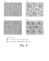
- a phosphor layer pattern is shown in Figs. 8A to 8E and Figs. 9A to 9D.
- a pattern of a phosphor layer which comprises first phosphor portions comprising green phosphor and second phosphor portions comprising red phosphor may be provided for the phosphor layer.
- the patterns shown in Figs. 8 and 9 are patterns in which the first phosphor portions are green and the second phosphor portions are red.
- a pattern is one in which the blue light emitted from the semiconductor light emitting element is transmitted and used as is without providing third phosphor portions which comprise blue phosphor.
- a pattern in which a light-shielding portion is provided at the interface between each of the phosphor portions is also possible.
- the pattern in which a light-shielding portion is provided at the interface between the light-shielding portions in Fig. 6B is shown in Fig. 10 .
- the phosphor layer of the present invention is preferably of a layer shape with a thickness of not more than 1 mm.
- the thickness is more preferably not more than 500 ⁇ m and even more preferably not more than 300 ⁇ m.
- the foregoing thickness does not include the thickness of the substrate in cases where the phosphor layer is formed on a transparent substrate which transmits near-ultraviolet light and visible light.
- the thickness of the phosphor layer in the present invention is not more than 1 mm and thin, fabrication is preferably straightforward by means of a method of coating phosphor on a transparent substrate which transmits visible light.
- the thickness of the phosphor layer can be measured by cutting the phosphor layer in the thickness direction and observing the cross section using an electron microscope such as an SEM.
- the combined thickness of the substrate coated with the phosphor layer and the phosphor layer is measured using a micrometer, and the thickness of the phosphor layer can be measured by using a micrometer to measure the thickness of the substrate once again after the phosphor layer has been detached from the substrate.
- the thickness can be measured directly by partially detaching the phosphor layer and using a stylus profile measuring system to measure the difference between the part where the phosphor layer remains and the part from which the phosphor layer has been detached part.
- a transparent substrate which transmits ultraviolet light and visible light there are no particular restrictions on the material of the substrate as long as the substrate is transparent to near-ultraviolet light and visible light, and glass and plastic (for example epoxy resin, silicone resin, acrylic resin, and polycarbonate resin or the like) can be used. If excited by wavelengths in the near-ultraviolet range, glass is preferable from the standpoint of durability.
- the thickness of the phosphor layer at least twice the volumetric basis median diameter of the phosphor contained in the phosphor layer and not more than 10 times this diameter preferably enables the self-absorption of the light of the phosphors and reduces the light scattering caused by the phosphors. If the thickness of the phosphor layer is too thin, since the excitation light from the semiconductor light emitting element is not adequately converted at the light emitting layer, there tends to be a drop in the intensity of the output light.
- the thickness of the phosphor layer is more preferably three times or more the median diameter of the phosphor and particularly preferably four times or more the median diameter.
- the thickness of the phosphor layer is preferably not more than nine times the median diameter of the phosphor, particularly preferably not more than eight times the median diameter, and more preferably not more than seven times the median diameter, and even more preferably not more than six times the median diameter, and most preferably not more than five times the median diameter.
- the volume fill rate of the phosphor in the phosphor layer is preferably at least 20% in order to raise the light emitting efficiency. If the volume fill rate drops below 20%, there is an increase in the light from the semiconductor light emitting element which is not excited by the phosphor at the light emitting layer and a risk of a drop in emission efficiency.
- the volume fill rate is more preferably at least 40%. Although there are no particular upper limit restrictions, there is normally no increase above the value for the maximum packing rate which is about 74%.
- the density of the phosphor layer is preferably at least 1.0 g/cm 3 .
- the phosphor layer of the present invention is preferably configured such that separate phosphor portions which are formed in a direction perpendicular to the thickness direction are disposed so as to prevent a reduction in overlapping parts in the thickness direction of the phosphor layer at the interface between the phosphor portions in order to be able to prevent cascade excitation and improve the emission efficiency. More specifically, the phosphor layer is preferably configured such that the proportion of the surface area of the part having phosphors of a plurality of types in the thickness direction of the phosphor layer relative to the light emission surface area of the light emitting device is 0% or more and 20% or less in order to improve the emission efficiency.
- light emission surface area of the light emitting device indicates the surface area of the part passing light emitted by the light emitting device to the outside, of the surface area of the light emitting device.
- surface area of the part having phosphors of a plurality of types in the thickness direction of the phosphor layer means the projection surface area when the part having phosphors of a plurality of types in the thickness direction of the phosphor layer is projected onto the surface on the emission direction side from the thickness direction of the phosphor layer.
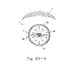
- Figs. 5-1 to 5-3 show the contact face of adjoining phosphor portions. At this contact face, there is a part where phosphors of a plurality of types overlap in the thickness direction of the phosphor layer. Cascade excitation occurs extremely readily in this overlap part. For this reason, the state in Fig. 5-1 is preferable over the state in Fig. 5-2 in enabling prevention of cascade excitation. Further, a configuration like that in Fig. 5-3 by means of a method such as providing a light-shielding portion between the phosphor portions is more preferable in enabling prevention of cascade excitation.
- the proportion of the surface area of the part where a plurality of phosphors exist is preferably not more than 10%, more preferably not more than 5%, and most preferably 0%.
- the light-shielding portion is preferably disposed so as to prevent the light emitted from the first phosphor portions from entering the second phosphor portions. Further, the light-shielding portion is preferably of a black matrix or reflective material and more preferably a reflective material.
- the desired interface between the first and second phosphor portions can be established to enable the foregoing numerical range for the overlap surface area by, for example, using screen printing, and (1) forming the first phosphor portions of a desired shape by using a screen of a specific shape, and (2) subsequently forming the second phosphor portions so as to contact the first phosphor portions.
- the desired shape for the interface between the first and second phosphor portions can be established to enable the foregoing numerical range for the overlap surface area by, for example, (1) forming a mask of a specific shape on the substrate by means of photolithography or the like, (2) forming first phosphor portions of the desired shape so as to adjoin the mask, (3) subsequently removing the mask, and (4) forming second phosphor portions, of the same shape as the removed mask, so as to contact the first phosphor portions in order to fill the part from which the mask was removed.
- the surface area of the overlap part where phosphors of a plurality of types overlap in the phosphor layer of the present invention can be measured by cutting the phosphor layer in a thickness direction and observing the cross section using an electron microscope such as an SEM.
- the phosphor layer of the present invention is fabricated by arranging a plurality of phosphor portions and hence there is a contact face formed by adjoining phosphor portions at a plurality of points.
- the surface area of the overlap part where phosphors of a plurality of types overlap is given by the sum of the surface areas of the overlap parts which exist in the light emission surface area of the light emitting device.
- the phosphor layer of the present invention comprises an area A comprising two or more 1Ath phosphor portions and two or more 2Ath phosphor portions and an area B comprising two or more 1Bth phosphor portions and two or more 2Bth phosphor portions.
- the condition of formula [1] below is satisfied when the sum total of the surface area occupied by the 1Ath phosphor portions in the area A is S A1 , the sum total of the surface area occupied by the 2Ath phosphor portions is S A2 , the sum total of the surface area occupied by the 1Bth phosphor portions in the area B is S B1 , and the sum total of the surface area occupied by the 2Bth phosphor portions is S B2 .
- the areas A and B are preferably provided as separate areas in a direction perpendicular to the thickness direction of the phosphor layer and are more preferably provided so as to adjoin one another as separate areas in a direction perpendicular to the thickness direction of the phosphor layer.
- the 1Ath phosphor contained in the 1Ath phosphor portions and the 1Bth phosphor contained in the 1Bth phosphor portions may be phosphors of the same type or phosphors of different types, but that the types are preferably different from the standpoint of precisely controlling the color temperature of the light emitted by the light emitting device.
- the 2Ath phosphor contained in the 2Ath phosphor portions and the 2Bth phosphor contained in the 2Bth phosphor portions may be phosphors of the same type or phosphors of different types.
- the second phosphor contained in the second phosphor portions emits light which includes a component of a longer wavelength than the light emitted by the first phosphor contained in the first phosphor portions. That is, there is a difference in wavelength of the fluorescent light emitted by the phosphors contained in the second phosphor portions and first phosphor portions, and the second phosphor portions emit fluorescent light of a longer wavelength.
- the semiconductor light emitting element emits light of a wavelength in the violet range
- the phosphor contained in the first phosphor portions is blue and the phosphor contained in the second phosphor portions is yellow.
- the phosphor contained in the first phosphor portions is green, the phosphor contained in the second phosphor portions is red, and the phosphor contained in the third phosphor portions is blue.
- the phosphor contained in the first phosphor portions is blue, the phosphor contained in the second phosphor portions is green, and the phosphor contained in the third phosphor portions is red.
- the phosphor contained in the first phosphor portions is blue, the phosphor contained in the second phosphor portions is red, and the phosphor contained in the third phosphor portions is green.
- the phosphor contained in the first phosphor portions is green, the phosphor contained in the second phosphor portions is red, the phosphor contained in the third phosphor portions is blue, and the phosphor contained in fourth phosphor portions is yellow. Further, the phosphor contained in the first phosphor portions is blue, the phosphor contained in the second phosphor portions is green, the phosphor contained in the third phosphor portions is red, and the phosphor contained in fourth phosphor portions is yellow. Furthermore, the phosphor contained in the first phosphor portions is blue, the phosphor contained in the second phosphor portions is red, the phosphor contained in the third phosphor portions is green, and the phosphor contained in fourth phosphor portions is yellow.
- the semiconductor light emitting element emits light of a wavelength in the blue color range
- the phosphor contained in the first phosphor portions is green, and the phosphor contained in the second phosphor portions is red.
- the phosphor contained in the first phosphor portions is green, the phosphor contained in the second phosphor portions is red, and the phosphor contained in the third phosphor portions is yellow. Note that, if the color rendering properties are to be improved, the phosphor contained in the first phosphor portions is green, the phosphor contained in the second phosphor portions is red, the phosphor contained in the third phosphor portions is red, and there is a difference in the type and peak wavelength of the phosphor between the second and third phosphor portions.
- the foregoing formula [1] represents different proportions for green phosphor and red phosphor in the areas A and B. That is, different emission spectra, for example, color temperatures of the emitted light color are represented in areas A and B.
- An area with a larger amount of red phosphor has a lower emitted light color temperature, that is, emits white light like that of a light bulb, and an area with a smaller amount of red phosphor has a higher emitted light color temperature, that is, emits pale white light like that of a fluorescent lamp.
- the color temperature of the emitted light color can be tuned by adjusting the proportion of the light irradiated onto areas A and B from the semiconductor light emitting element, in the phosphor layer. Accordingly, simply by adjusting the ratio between the surface areas of the first phosphor portions and second phosphor portions contained in areas A and B in the phosphor layer, it is possible to easily adjust the emission spectrum of the light which is a combination of the light emitted from area A and the light emitted from area B.
- the light emitting device is configured using the phosphors and the semiconductor light emitting element and the emission spectrum of the light emitting device can easily be tuned by adjusting the proportion of the light irradiated onto areas A and B from the semiconductor light emitting element.
- the phosphor layer of the present invention further comprises an area X between the area A and the area B,
- Fig. 13-1 if the surface areas of areas A, B, and X are the same as the light emission surface area of the light emitting device and the areas are provided so as to adjoin one another, when the phosphor layer or the semiconductor light emitting element is moved, as shown in Fig. 13-2A if the light emission area matches area A, the light emitted from area A is the light emitted by the light emitting device, 13-2B if the light emission area matches area X, only the light emitted from area X is the light emitted by the light emitting device, and 13-2C if the light emission area matches the area B, only the light emitted from area B is the light emitted by the light emitting device.
- the phosphor layer is configured as per Fig. 13-1 , by moving the phosphor layer or the semiconductor light emitting element, it is possible to continuously adjust the color temperature of the light emitted by the light emitting device to an optional color temperature, in the chromaticity diagram, which lies on a straight line linking a color temperature A (X A , y A ) of the light emitted from area A and a color temperature X (X x , y x ) of the light emitted from area X or linking a color temperature B (X B , y B ) of the light emitted from area B and a color temperature X ( x X, y x) of the light emitted from area X.
- an optional color temperature in the chromaticity diagram, which lies on a straight line linking a color temperature A (X A , y A ) of the light emitted from area A and a color temperature X (X x , y x ) of the light emitted from
- the color temperature X (X x , y x ) may lie on a straight line linking the color temperature A (x A , y A ) and the color temperature B(X B , y B ) and, as shown in Fig. 14-1B , the color temperature X (X x , y x ) may not lie on a straight line linking the color temperature A (x A , y A ) and the color temperature B(X B , y B ).
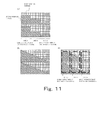
- the phosphor layer is disposed in order to enable adjustment to an optional color temperature which lies on a straight line linking the color temperature A of the light emitted from area A and the color temperature X of the light emitted from area X or an optional color temperature which lies on a straight line linking the color temperature B of the light emitted from area B and the color temperature X of the light emitted from area X is shown in Figs. 11A to 11C and Figs. 12A to 12D.
- the areas A, B, and X in the phosphor layer may be provided clearly marked as per Fig. 11A or may be provided without being clearly marked as per Fig. 11B .
- optional ranges which comprises two or more first phosphor portions and two or more second phosphor portions can each be assigned to areas A, B, and X.
- the first phosphor portions and second phosphor portions in the phosphor layer may be provided so as to span the areas A, B, and X as per Fig. 11C .
- the phosphor layer is configured as per Figs. 15A and 15B , by moving the phosphor layer or semiconductor light emitting element, it is possible to continuously adjust the color temperature of the light emitted by the light emitting device to an optional color temperature, in the chromaticity diagram, which lies on a curve linking a color temperature A (X A , y A ) of the light emitted from area A, a color temperature X (X x , y x ) of the light emitted from area X, and a color temperature B (X B , y A ) of the light emitted from area B.
- an optional color temperature in the chromaticity diagram, which lies on a curve linking a color temperature A (X A , y A ) of the light emitted from area A, a color temperature X (X x , y x ) of the light emitted from area X, and a color temperature B (X B , y A ) of the light emitted from
- the color temperature of the light emitted by the light emitting device can be continuously adjusted along a black-body radiation curve by aligning the color temperature A, color temperature X, and color temperature B on a black-body radiation curve. Further, by setting the color temperatures A, X, and B at a slight displacement from the black-body radiation curve, for example by setting the deviation duv from the black-body radiation curve as -0.02 ⁇ duv ⁇ 0.02, the color temperature of the light emitted by the light emitting device can be continuously adjusted in a range where the deviation duv from the black-body radiation curve is -0. 02 ⁇ duv ⁇ 0.02, where duv is a value defined according to JIS Z 8725:1999.
- the phosphor layer of the present invention may also be afforded a desirable aspect based on thickness rather than the surface area of the phosphor portions. More specifically, the phosphor layer of the present invention preferably satisfies the condition of formula [2] below when the sum total of the thickness of the 1Ath phosphor portion of area A is T A1 , the sum total of the thickness of the 2Ath phosphor portions of area A is T A2 , the sum total of the thickness of the 1Bth phosphor portions of area B is T B1 , and the sum total of the thickness of the 2Bth phosphor portions of area B is T B2 .
- formula [2] above represents different proportions for green phosphor and red phosphor in the areas A and B. That is, different emission spectra, for example, color temperatures of the emitted light color are represented in areas A and B.
- An area with a larger amount of red phosphor has a lower emitted light color temperature, that is, emits white light like that of a light bulb, and an area with a smaller amount of red phosphor has a higher emitted light color temperature, that is, emits pale white light like that of a fluorescent lamp.
- the color temperature of the emitted light color can be tuned by adjusting the proportion of the light irradiated onto areas A and B from the semiconductor light emitting element, in the phosphor layer. Accordingly, simply by adjusting the ratio between the thicknesses of the first phosphor portions and second phosphor portions contained in areas A and B in the phosphor layer, it is possible to easily adjust the emission spectrum of the light which is a combination of the light emitted from area A and the light emitted from area B.
- the light emitting device is configured using the phosphors and the semiconductor light emitting element and the emission spectrum of the light emitting device can easily be tuned by adjusting the proportion of the light irradiated onto areas A and B from the semiconductor light emitting element.
- S A1 , S A2 , S B1 , and S B2 , and T A1 , T A2 , T B1 , and T B2 can be obtained by using an optical microscope to measure the surface area occupied by each of the phosphor portions in each area of the phosphor layer, on the face on the light-emission side of the light emitting device, or by measuring the cross section of the phosphor layer using an optical microscope.
- the semiconductor light emitting element of the present invention emits the excitation light of the phosphor contained in the first phosphor portions and second phosphor portions.
- the wavelength of the excitation light is 350 nm or more and 520 nm or less, preferably at least 370 nm, and more preferably at least 380 nm. Further, this wavelength is preferably not more than 500 nm and more preferably not more than 480 nm.
- a light emitting device with superior color rendering properties can preferably be provided.
- the semiconductor light emitting element which may be given include semiconductor light emitting elements which use a InGaAlN, GaAlN or InGaAlN semiconductor or similar for which crystal growth is performed using the MOCVD method or the like on a silicon carbide, sapphire, or gallium nitride substrate.
- a plurality of semiconductor light emitting elements are preferably used aligned in a planar shape.
- the present invention is preferably used in a light emitting device which comprises such a large emission surface area.
- the light emitting device of the present invention can comprise a package for holding a semiconductor light emitting element and which has an optional shape and material.
- Specific shapes which can be used are plate shape, cup shape, or any suitable shape depending on the application. Among these shapes, a cup-shaped package is preferable since this shape is able to retain directivity in the light emission direction and is able to effectively use the light emitted by the light emitting device.
- the surface area of the opening for emitting light is preferably 20% or more and 600% or less of the base surface area.
- possible package materials which can be used include suitable materials depending on the application such as inorganic materials such as metals, glass alloys and carbons, and organic materials such as synthetic resins.
- Highly reflective packages of this type include packages which are formed of silicone resin and which comprise light scattering particles. Possible examples of light scattering particles include titania and alumina.
- the light emitting device of the present invention can also comprise a bandpass filter on the semiconductor light emitting element side of the light emitting device and/or on the light emission direction side of the light emitting device.
- a bandpass filter possesses the property of passing only light of predetermined wavelengths and enables control of the light emission in the near-ultraviolet and ultraviolet ranges from the light emitting device.
- Commercial bandpass filters can suitably be used in the present invention, where the type of bandpass filter is suitably selected according to the type of semiconductor light emitting element.
- metal wiring for supplying power from the outside to the semiconductor light emitting element and a cap to protect the light emission direction side of the phosphor layer, and so on, can be suitably disposed.
- the light emitting device of the present invention comprises an area A and an area B with different emission spectra in the phosphor layer, for example different emitted light color temperatures, and the emission spectrum of the light emitted by the light emitting device can be continuously tuned by adjusting the proportion of the light irradiated onto the areas A and B from the semiconductor light emitting element.
- the phosphor layer or semiconductor light emitting element may be moved so as to change the relative positional relationship between the phosphor layer and semiconductor light emitting element, for example, the phosphor layer or semiconductor light emitting element may be moved in a direction perpendicular to the thickness direction of the phosphor layer.
- the semiconductor light emitting element may comprise a light distribution member such as a light distribution lens and the tilt angle of the optical axis of the light distribution member relative to the thickness direction of the phosphor layer may be adjusted.
- reflective-type light emitting device may be adopted in which the light emitted by the semiconductor light emitting element falls incident on the reflective member once and the light reflected by the reflective member is introduced to the phosphor layer, and the tilt angle of the optical axis of the light reflected by the reflective member relative to the thickness direction of the phosphor layer may be adjusted.
- a semiconductor light emitting element A and a semiconductor light emitting element B may be provided in areas A and B respectively and the amount of power fed to the respective semiconductor light emitting elements may be adjusted.
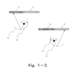
- Fig. 1-1 the light emission area is adjusted by moving the phosphor layer perpendicularly to the thickness direction of the phosphor layer but, as shown in Fig.
- the light emission area can be adjusted by providing a configuration in which a light distribution member comprising a rotational axis is installed between the semiconductor light emitting element and the phosphor layer so that the light distribution member is able to turn about the rotational axis.
- the light emission area can also be adjusted by providing a configuration in which a semiconductor light emitting element is disposed such that the light from the semiconductor light emitting element does not strike the phosphor layer directly and a reflective member comprising a rotational axis is disposed so that the light emitted by the semiconductor light emitting element can be reflected toward the phosphor layer and the reflective member is able to turn about the rotational axis.
- a light distribution member comprising a rotational axis is installed between the semiconductor light emitting element and the phosphor layer so that the light distribution member is able to turn about the rotational axis.
- the light emission area can also be adjusted by providing a configuration in which a semiconductor light emitting element is disposed such that the light from the semiconductor light emitting
- a semiconductor light emitting element A and a semiconductor light emitting element B may be provided in areas A and B respectively and the amount of power fed to the respective semiconductor light emitting elements may be adjusted.
- a plurality of semiconductor light emitting elements can be provided in each of the areas A and B, for example four semiconductor light emitting elements A and four semiconductor light emitting elements B, and the proportion of light irradiated onto the areas A and B can be adjusted by turning on some of the semiconductor light emitting elements and turning off the other semiconductor light emitting elements.
- Fig. 1-5A in a case where only four semiconductor light emitting elements, provided directly below area A, are turned on, light is emitted from the area A; as per Fig.
- Area A and area B of the phosphor layer are areas of different emission spectra for the light emitted from the respective areas. Hence, because the emission spectrum of the light emitted from the light emitting device can be continuously adjusted by changing the proportions of the area A and area B which occupy the optical emission area of the light emitting device, a light emitting device which emits light of the desired emission spectrum can be provided.
- Suitable aspects of areas A and B according to the present invention include suitable combinations of the following aspects (a) to (c), for example:
- the phosphor layer of the present invention which comprises such areas A and B is designed to be larger than the light emission surface area of the light emitting device, by moving the phosphor layer so as to change the relative positions of the phosphor layer and semiconductor light emitting element, it is possible to adjust the proportions of light of two types of different spectra in the light emitted from area A and the light emitted from area B. More specifically, by moving the phosphor layer in a direction perpendicular to the thickness direction of the phosphor layer, it is possible to adjust the proportions of two types of light of different emission spectra in the light emitted from area A and the light emitted from area B.
- the emission spectra can also be adjusted by moving the semiconductor light emitting element (the package is a package is provided). Further, in a case where the light emitting device comprises a housing member, described subsequently, the proportion of the light which is irradiated onto areas A and B from the semiconductor light emitting element can be adjusted by rotationally moving the housing member about the semiconductor light emitting element, and this can also be achieved by rotating the semiconductor light emitting element, and so on.
- Possible means for moving or rotationally moving the phosphor layer and/or the semiconductor light emitting element include driving by means of a manual operation, an actuator, and a motor, and the like.
- the movement direction may either be linear motion or rotational motion.
- the phosphor layer of the present invention enables continuous adjustment of the color temperature of the white light from 2800 K to 6500 K by means of a relative changing of the positional relationship between the semiconductor light emitting element and the phosphor layer which comprises areas A and B.
- Fig. 1-1 shows a schematic diagram of an overall view of a light emitting device 1 of the present invention.
- the light emitting device 1 is a light emitting device in which a semiconductor light emitting element 2 is disposed on a flat face, and the semiconductor light emitting element 2 is disposed on the bottom face of a hollow portion of a package 3. Further, a phosphor layer 4 is disposed in an opening in the package 3.
- a near-ultraviolet semiconductor light emitting element which emits light of a wavelength in the near-ultraviolet range
- a violet semiconductor light emitting element which emits light of a wavelength in the violet color range
- a blue semiconductor light emitting element which emits light of a wavelength in the blue color range
- a violet semiconductor light emitting element will be described by way of example.
- a single semiconductor light emitting element may be installed or a plurality of semiconductor light emitting elements may be disposed in a planar shape.
- the light emitting device can also be configured by installing a single large-output semiconductor light emitting element.
- configuring a light emitting device either by disposing a plurality of semiconductor light emitting elements in a planar shape or by installing a single large-output semiconductor light emitting element permits straight-forward surface lighting and is therefore preferable.
- the package 3 holds the semiconductor light emitting elements and phosphor layer and, in this embodiment, is cup-shaped with an opening and a hollow portion, and the semiconductor light emitting element 2 is disposed on the bottom face of the hollow portion. If the package 3 is cup-shaped, the directivity of the light emitted from the light emitting device can be retained and the emitted light can be better used.
- the specifications of the hollow portion of the package 3 are set as specifications enabling the light emitting device 1 to emit light in a predetermined direction.
- the bottom portion of the hollow portion of the package 3 comprises electrodes (not shown) for supplying power to the semiconductor light emitting element from the outside of the light emitting device 1.
- a highly reflective package is preferably used for the package 3, thereby enabling the light striking the wall surface (tapered portion) of the package 3 to be emitted in a predetermined direction and making it possible to prevent a loss of light.
- the phosphor layer 4 is disposed at the opening of the package 3.
- the hollow portion of the package 3 is covered by the phosphor layer 4 and the light from the semiconductor light emitting element 2 does not pass through the phosphor layer 4 and is not emitted from the light emitting device 1.
- the phosphor layer 4 comprises three areas, namely an A area 4a, an X area 4x, and a B area 4b which have different emission spectra, and the size of the phosphor layer 4 is designed to be larger than the size of the opening of the package 3.
- the phosphor layer 4 which is of a greater surface area than the opening of the package 3 while covering the opening of the package 3 (the arrow 8 in the drawing is an example of the horizontal sliding direction of the phosphor layer 4), it is possible to adjust the proportion of light irradiated onto area A and area B from the semiconductor light emitting element 2 and to adjust the emission spectra of the light emitted by the light emitting device 1.
- the package 3 may also be slid horizontally without horizontally sliding the phosphor layer 4.
- the color temperature of the emitted light of the A area 4a of the phosphor layer is in a 6500 K high color temperature range
- the color temperature of the emitted light of the B area 4b is in a 2800 K low color temperature range
- the color temperature of the emitted light of the X area 4x is a middle color temperature range of 4500 K
- the surface areas of the areas A, B, and X are each the same as that of the opening of the package
- a pale white light with a color temperature of 6500 K is emitted if the opening of the package 3 is completely covered by the A area 4a of the phosphor layer
- a white light with a color temperature of approximately 3700 K which is intermediate between 2800 K and 4500 K is emitted if the opening of the package 3 is covered approximately by a half each by the A area 4a and the X area 4x.
- a white light of a color temperature of approximately 5500 K which is intermediate between 4500 K and 6500 K is emitted if the opening is covered approximately by a half each by the X area 4X and the B area 4b.
- a white light like that of a light bulb with a color temperature of 2800 K is emitted if the opening of the package 3 is completely covered by a B area 4b.
- the color temperature of the emitted light can be continuously adjusted by moving the area of the phosphor layer which covers the opening of the package 3, a light emitting device which emits light of the desired color temperature can be provided.
- Fig. 2 shows a detailed schematic diagram of the phosphor layer 4.
- the phosphor layer 4 is formed on a transparent substrate 5 which transmits near-ultraviolet light and visible light. Using the transparent substrate 5 enables screen printing and the formation of the phosphor layer 4 is straightforward.
- the phosphor layer 4 which is formed on the transparent substrate is a layer with a thickness of not more than 1 mm and comprises the first phosphor portion 6a to the third phosphor portion 6c.
- the first phosphor portion 6a is a phosphor portion which comprises a green phosphor 7a in this embodiment, and emits light in the green color range which is a longer component than the light in the violet color range as a result of being excited by the light of the violet semiconductor light emitting element 2.
- the second phosphor portion 6b is a phosphor portion which comprises a red phosphor in this embodiment and emits light in the red color range which is a longer component than the light in the green color range emitted by the green phosphor contained in the first phosphor portion as a result of being excited by the light of the violet semiconductor light emitting element 2.
- the third phosphor portion 6c is a phosphor portion which comprises a blue phosphor in this embodiment and is provided in order to generate white light.
- the phosphor portions are suitably selected according to the types of semiconductor light emitting element used, with the foregoing third phosphor portion being unnecessary in a case where a blue semiconductor light emitting element is used because the light from the blue semiconductor light emitting element can be used as is as blue light for generating white light.
- the phosphor portions are each provided such that the surface area of the part with a plurality of types of phosphor in the thickness direction of the phosphor layer is 0% or more and 20% or less of the light emission surface area of the light emitting device of the phosphor layer, that is, of the surface area of the opening of the package 3. Since there is a plurality of phosphor portions in the light emission surface area, the surface area of the part with a plurality of types of the foregoing phosphor is calculated as the sum total of the surface areas of the plurality of parts.
- a bandpass filter 9 can be provided on the light emission side and/or the semiconductor light emitting element side of the light emitting device of the phosphor layer 4.
- the "light emission side of the light emitting device of the phosphor layer 4" indicates, of the surface in a direction perpendicular to the thickness direction of the phosphor layer 4, the side of the surface from which light is emitted to the outside of the light emitting device, that is, using Fig. 3 to illustrate, the upper part of the phosphor layer 4.
- the semiconductor light emitting element side of the phosphor layer 4" indicates, of the surface in a direction perpendicular to the thickness direction of the phosphor layer 4, the surface side from which light is emitted to the inside of the light emitting device, that is, using Fig. 3 to illustrate, the lower part of the phosphor layer 4.
- the bandpass filter 9 possesses the property of passing only light of predetermined wavelengths, and by providing a bandpass filter, which reflects at least a portion of the light emitted by the semiconductor light emitting element and transmits at least a portion of the light emitted by the phosphor, between the package 3 and the phosphor layer 4, the fluorescent light emitted by the phosphor can be prevented from entering the package once again, thereby raising the emission efficiency of the light emitting device.
- the bandpass filter which reflects at least a portion of the light emitted by the semiconductor light emitting element and transmits at least a portion of the light emitted by the phosphor, on the light emission side of the light emitting device of the phosphor layer 4, the light emitted by the semiconductor light emitting element which is not absorbed by the phosphor and passes through can be returned once again to the phosphor layer to excite the phosphor, thereby raising the emission efficiency of the light emitting device.
- the bandpass filter is suitably selected according to the semiconductor light emitting element 2. Further, as per Fig.
- the proportion of the light which enters in the thickness direction of the bandpass filter can be increased, thereby enabling the bandpass filter to be used more efficiently.
- Fig. 4 show a schematic diagram of another embodiment for the installation of the semiconductor light emitting element 2, the package 3, and the phosphor layer 4.
- Fig. 4A is an embodiment of Fig. 1 , and is an embodiment in which the phosphor layer 4 is disposed in the opening of the package 3. The disposition is designed to enable the phosphor layer 4 or the package 3 to move in the arrow direction. The light emitted by the semiconductor light emitting element 2 is converted into fluorescent light of the phosphor layer 4 and is emitted outside the device.
- Fig. 4B shows an aspect in which disposition is such that the periphery of the semiconductor light emitting element 2 is covered by the phosphor layer 4.
- the disposition is such that the phosphor layer 4 can be moved in the arrow direction and the package 3 can be moved in the arrow direction.
- the light emitted by the semiconductor light emitting element 2 is converted into fluorescent light in the phosphor layer 4 and is emitted outside the device.
- Fig. 4C shows an aspect in which the phosphor layer 4 is placed on the surface of the package 3 and the semiconductor light emitting element 2 is held by a transparent member which is provided in the opening so as to emit light in a downward direction in the drawing.
- Installation is such that the phosphor layer 4 can be moved in the arrow direction along the shape of the hollow portion of the package 3 and such that the semiconductor light emitting element 2 can be moved in the direction of the arrow.
- the light which is emitted from the semiconductor light emitting element 2 is fluorescent light in the phosphor layer 4, and the fluorescent light is reflected by the package 3 comprising the reflective member and emitted outside the device.
- the semiconductor light emitting element 2 and phosphor layer 4 are a distance apart, and this distance is preferably at least 0.1 mm, more preferably at least 0.3 mm, even more preferably at least 0. 5 mm, and particularly preferably at least 1 mm, and preferably not more than 500 mm, more preferably not more than 300 mm, even more preferably not more than 100 mm, and particularly preferably not more than 10 mm.
- this arrangement it is possible to prevent a weakening of the excitation light for each unit area of the phosphor and degradation of the light of the phosphor, and even if the temperature of the semiconductor light emitting element rises, a rise in the temperature of the phosphor layer can be alleviated.
- Fig. 16 is a perspective view schematically showing the overall configuration of the light emitting device 1 according to the first embodiment.
- the light emitting device 11 is a light emitting device which uses a light emitting diode as the light source and enables the color temperature of the output light to be adjusted.
- the light emitting device 11 is a white light emission device which permits the selective output of daylight color or light bulb color light.
- the light emitting device 11 comprises, as main members, a light emitting diode (LED) 12, a substrate 13 whereon the light emitting diode 12 is disposed, and a cylindrical housing member 14 in which the substrate 13 is housed.
- the light emitting diode 12 corresponds to the semiconductor light emitting element of the present invention.
- the housing member 14 comprises a cylindrical shape.
- the housing member 14 may also be formed as a polygonal cylindrical shape.
- the center axis of the housing member 14 is denoted by the reference sign CA.
- An end face opening 143 is open at both ends of the housing member 14.
- the interior of the housing member 14 houses the substrate 13 which comprises a rectangular flat plate shape.
- the substrate 13 is integrally fixed to a fixed member for fixing the light emitting device 11 to an attachment target such as a ceiling, for example.
- an attachment target such as a ceiling
- the substrate 13 is fixed to the ceiling and adopts an idle posture.
- the substrate 13 is a circuit substrate printed with a circuit for supplying power from the outside to the light emitting diodes 12.
- an illustration of the circuit for controlling the power supplied to the light emitting diodes 12 is omitted.
- the light emitting diodes 12 are arranged along the longitudinal direction of the substrate 13.
- the longitudinal direction of the substrate 13 as it is intended here matches the direction along the center axis CA of the housing member 14.
- the disposition example of the light emitting diode 12 shown is for illustrative purposes and the disposition is not limited to this example.
- a single light emitting diode 12 may also be mounted on the substrate.
- the housing member 14 is formed of phosphor material. More specifically, a phosphor layer 141 which comprises phosphor which is excited by the excitation light emitted by the light emitting diode 12 is formed on the housing member 14.
- the phosphor layer 141 comprises a phosphor as described earlier and converts the light from the light emitting diode 12 to a longer wavelength light and emits the light to the outside of the housing member 14.
- the phosphor layer 141 is configured comprising a plurality of phosphor areas of different emission spectra as will be described subsequently.
- the housing member 14 is configured by coating various phosphors on a base material which possesses transparency for transmitting near-ultraviolet light and visible light.
- a base material which possesses transparency for transmitting near-ultraviolet light and visible light.
- materials which can be used for the transparent base material as long as the material is transparent to near-ultraviolet light and visible light, and glass and plastic (for example epoxy resin, silicone resin, acrylic resin, polycarbonate resin and the like) and so on can be used. Glass is preferable from the standpoint of durability in the case of excitation with wavelengths in the near-ultraviolet range.
- the light emitting diode 12 is a semiconductor light emitting element which emits the excitation light of the phosphor contained in the phosphor layer 141.
- the phosphor coated on the transparent base material of the housing member 14 can be suitably selected according to the wavelength of the light emitted by the light emitting diode 12.
- the light emitting device 11 irradiates the excitation light emitted by the light emitting diode 12 onto various phosphors contained in the phosphor layer 141. The light emitting device 11 then emits white light to the outside by emitting light of a longer wavelength than the excitation light from the phosphor.
- Fig. 17 schematically shows a cross section in a direction orthogonal to the center axis CA shown in Fig. 16 (hereinafter called a "axis orthogonal cross section").
- the light emitting diode 12 is provided only on one side of the substrate 13 (on the lower edge of the bottom face in the drawing).
- the substrate 13 is housed in the housing member 14 such that the center position in the thickness direction of the substrate 13 coincides with the center axis CA of the housing member 14.
- the arrows indicated by a broken line in the drawing schematically indicate the directions of the light emitted by the light emitting diode 12.
- the arrow to which reference sign Dc is assigned represents an irradiation center direction.
- the irradiation center direction Dc signifies the center direction of the excitation light irradiated with directivity.
- the light emitting device 11 described in this embodiment is provided on a ceiling such that the orientation of the substrate 13 in the housing member 14 is parallel to the ceiling. Of the faces of the substrate 13, the face facing the ceiling is called the “upper face” and the other face is called the “lower face.”
- the irradiation target area in this embodiment is below the light emitting device 11 and hence the light emitting diode 12 is disposed on the lower face of the substrate 13.
- the light emitting diode 12 may be disposed on both the upper face and lower face of the substrate 13.
- a configuration for modifying the color temperature of the output light in the light emitting device 11 according to the present invention will be described next.
- daylight color and light bulb color which have relatively different color temperatures, are suitably selected and output will be described by taking, by way of example, a case where the wavelength of the excitation light of the light emitting diode 12 is in the near-ultraviolet range or violet range.
- Fig. 18 is a development view of the housing member 14 which has a cylindrical shape.
- Reference sign 142 represents the transparent base material.
- the transparent base material forms a rectangular shape in a developed state as shown.
- the positions 0° (12 o'clock), 90° (3 o'clock), 180° (6 o'clock), and 270° (9 o'clock) of the developed state in Fig. 18 each correspond to the same positions in the cylindrically molded state in Fig. 17 .
- Phosphor which is excited by the light emitted by the light emitting diode 12 is coated on the surface of the transparent base member.
- the excitation light emitted by the light emitting diode 12 is near-ultraviolet light or ultraviolet light, and hence blue, green, and red phosphors are mixed together and coated on the transparent base material.
- the various phosphors may be formed, for example, by forming a phosphor paste on the transparent base material using screen printing or using inkjet printing, or may be formed using a transfer process or by using an exposure-type coating method which is used to coat a Cathode Ray Tube (CRT), or the like.
- the phosphor layer 141 may also be formed on the transparent base material by means of other methods.
- the area on the transparent base material is divided into two parts, namely, a first fluorescent area (area A) FCA and a second fluorescent area (area B) SCA.
- the first fluorescent area (area A) FCA has a high blue phosphor content in comparison with the second fluorescent area (area B) SCA.
- the first fluorescent area (area A) FCA has a low red or green phosphor content in comparison with the second fluorescent area (area B) SCA.
- the emission spectrum of light emitted by the first fluorescent area (area A) FCA as a result of the excitation light from the light emitting diode 12 is short in comparison with the emission spectrum in the second fluorescent area (area B) SCA. Accordingly, the color temperature of the emission color in the first fluorescent area (area A) FCA can be set high in comparison with the second fluorescent area (area B) SCA.
- the color temperature of the emission color of the first fluorescent area (area A) FCA can be made a 6500 K high color temperature area and daylight color white light may be emitted from this area.
- the color temperature of the emission color of the second fluorescent area (area B) SCA may be in a 2800 K low color temperature area, for example, and light bulb color white light may be emitted from this area.
- phosphor portions on which blue, green, and red phosphors are individually coated may be disposed on a transparent base material, for example.
- the phosphor portions each have a phosphor of a single type and various shapes and layout patterns may be adopted. Further, color mixing is possible by adjusting the ratio between the surface areas of the phosphor portions containing these phosphors.
- the color temperature of the emission color in the first fluorescent area (area A) FCA may be set higher than the second fluorescent area (area B) SCA.
- the phosphor layer 141 comprises a plurality of fluorescent areas of different emission spectra and which are formed in different positions in a peripheral direction of the housing member 14.
- the plurality of fluorescent areas divide the phosphor layer 141 in the peripheral direction and are formed as areas along the direction of the center axis CA of the housing member 14.
- the phosphor layer 141 comprises a first fluorescent area (area A) FCA and a second fluorescent area (area B) SCA which have mutually different emission spectra is described.
- the first fluorescent area (area A) FCA and the second fluorescent area (area B) SCA are disposed so as to divide the phosphor layer 141 into two equal parts in the peripheral direction.
- the first fluorescent area (area A) FCA is formed in an area which corresponds to an angle about the center axis CA of the housing member 14 of 270° to 90°
- the second fluorescent area (area B) SCA is formed in a range corresponding to 90° to 270°.
- the housing member 14 is provided turnably about the center axis CA in a state where the substrate 13 is fixed.
- An axle-like protruding member 131 which is co-axial to the center axis CA is protrudingly provided on the substrate 13 so as to extend from the short edge toward the end face opening 143, and a ring-like axle support member 132 is turnably supported by the axle-like protruding member 131.
- the axle-like protruding member 131 and the axle support member 132 are indicated by broken lines.
- the axle-like protruding member 131 and axle support member 132 are provided on both the short edges of the substrate 13.
- the housing member 14 is connected via a connecting member (not illustrated) to the axle support member 132. Therefore, the housing member 14, which is integrally connected to the axle support member 132, also turns about the axle-like protruding member 131 as a result of the axle support member 132 turning about the axle-like protruding member 131.
- the axle-like protruding member 131 is provided integral to the substrate 13. Accordingly, the housing member 14 can be made to turn about the center axis CA in a state where the substrate 13 is idle by causing the axle support member 132 to turn about the axle-like protruding member 131. That is, the housing member 14 can be made to turn relative to the substrate 13.
- Means which can be suitably adopted as means for causing the axle-like protruding member 131 to turn relative to the axle support member 132, that is, means for causing the housing member 14 to turn relative to the substrate 13, include driving means such as manual operation, an actuator, and a motor.
- driving means such as manual operation, an actuator, and a motor.
- a pull (cord) switch system can be adopted, for example. In this case, each time the pull switch is switched by means of a user switching operation, the housing member 14 comes to turn 180° about the center axis CA.
- Figs. 19A and 19B are switched each time there is a pull switch operation.
- Fig. 19A shows a state where the irradiation center direction Dc of the excitation light from the light emitting diode 12 coincides with the 12 o'clock (0°) direction and the first fluorescent area FCA is excited by the excitation light of the light emitting diode 12.
- Fig. 19B shows a state where the irradiation center direction Dc coincides with the 6 o'clock (180°) direction, and the second fluorescent area (area B) SCA is excited by the excitation light of the light emitting diode 12.
- the target fluorescent area which is irradiated with the excitation light emitted by the light emitting diode 12 can be selectively switched between either of the first fluorescent area (area A) FCA and the second fluorescent area (area B) SCA.
- the excitation light can be converted to daylight color white light and emitted to the outside from the housing member.
- light bulb color white light can be emitted by irradiating the second fluorescent area (area B) SCA with the excitation light from the light emitting diode 12.
- a gradation pattern of the first fluorescent area (area A) FCA and the second fluorescent area (area B) SCA in an area of a predetermined angle which is centered on the interface portion between the first fluorescent area (area A) FCA and the second fluorescent area (area B) SCA in the phosphor layer 141 may be formed having a gradation pattern of the first fluorescent area (area A) FCA and the second fluorescent area (area B) SCA.
- the foregoing gradation pattern is formed in an angular range between roughly 6 o'clock and 12 o'clock.
- the surface area ratio of the first fluorescent area (area A) FCA relative to the second fluorescent area (area B) SCA increases in moving from a 6 o'clock position to a 12 o'clock position.
- Fig. 20A is a pattern in which the first fluorescent area (area A) FCA and the second fluorescent area (area B) SCA are arranged alternately in stripes, and the surface area ratio of the first fluorescent area (area A) FCA relative to the second fluorescent area (area B) SCA is gradually changed by changing the angle of the stripes according to the position in the peripheral direction of the housing member 14.
- Fig. 20B is a pattern in which the first fluorescent area (area A) FCA and the second fluorescent area (area B) SCA are disposed with a triangular distribution
- Fig. 20C is a pattern in which the first fluorescent area (area A) FCA and the second fluorescent area (area B) SCA are arranged in dots. In all these patterns, the surface area ratio of the first fluorescent area (area A) FCA relative to the second fluorescent area (area B) SCA is gradually changed according to the position in the peripheral direction of the housing member 14.
- means for turning the housing member 14 about the center axis CA such as a pull switch, actuator, or motor (hereinafter these are referred to as “turning means") are preferable when the turn angle can be adjusted in a single step.
- turning means such as a pull switch, actuator, or motor
- the color temperature of white light emitted from the light emitting device 11 can be precisely adjusted by fine-tuning the turn angle of the housing member 14.
- the color temperature of the output light can be easily adjusted. Further, since there is a single power system for supplying power to the light emitting diode 12, there is no need for complex power control and a complex power circuit is also unnecessary. Hence, a light emitting device capable of color temperature adjustment can be manufactured at low cost.
- the phosphor layer 141 of the housing member 14 is formed over the whole circumferential face of the housing member 14, there is superior conversion efficiency of the excitation light emitted by the light emitting diode 12. That is, the aspect of the phosphor layer 141 can be suitably changed as long as the target for irradiation with the excitation light from the light emitting diode 12 can be switched between the first fluorescent area (area A) FCA and the second fluorescent area (area B) SCA by turning the housing member 14 in a peripheral direction. Accordingly, the phosphor layer 141 may also be formed on only part of the housing member 14.
- first fluorescent area (area A) FCA and second fluorescent area (area B) SCA) in the phosphor layer 141 is formed parallel to the center axis CA of the housing member 414. Therefore, when excitation light is emitted from each of the light emitting diodes 12 disposed side by side in the longitudinal direction of the substrate 13, irradiation of a different fluorescent area with the excitation light can be more reliably avoided. It is therefore possible to suppress simultaneous excitation of the first fluorescent area (area A) FCA and the second fluorescent area (area B) SCA which have different emission spectra.
- first fluorescent area (area A) FCA and the second fluorescent area (area B) SC in the phosphor layer 141 may be formed so that the size of the area occupied by each fluorescent area is different. Further, the phosphor layer 141 may be formed on the outer peripheral side of the transparent base material of the housing member 14, or may be formed on the inner peripheral side thereof. Further, the phosphor layer 141 may be formed on the inside of the transparent base material instead of on the surface thereof.
- COB chip on board
- first fluorescent area (area A) FCA and a second fluorescent area (area B) SCA are formed by mixing three types of phosphors, namely, red, blue and green
- the present invention is not limited to such an arrangement, rather, phosphors of other types may also be used.
- phosphors of two types, namely, blue and yellow may also be mixed together.
- the blue phosphor content in the first fluorescent area (area A) FCA may be set relatively high in comparison with the second fluorescent area (area B) SCA and the yellow phosphor content in the first fluorescent area (area A) FCA may be set relatively low in comparison with the second fluorescent area (area B) SCA.
- the color temperature of the light emitted to the outside can be raised in comparison with a case where the excitation light is irradiated onto the second fluorescent area (area B) SCA.
- the blue color light uses the light emitted by the light emitting diode 12 as is and a red phosphor and green phosphor or the like may be selected for the phosphor layer 141.
- the blue light component transmits through parts where the green and red phosphors or similar are not applied.
- the surface area ratio of the parts where phosphor is not applied in the first fluorescent area (area A) FCA may be set relatively high in comparison with that for the second fluorescent area (area B) SCA.
- the color temperature of the light emitted to the outside can be raised in comparison with a case where the excitation light is irradiated onto the second fluorescent area (area B) SCA.
- Figs. 21-1 to 21-5 are explanatory diagrams serving to illustrate modifications of the housing member 14 according to this embodiment.
- Each diagram shows an axis orthogonal cross section of the light emitting device 11 and corresponds to Fig. 17 . Note that illustrations of some members such as the axle-like protruding member 131 and axle support member 132 have been omitted from each diagram.
- Figs. 21-1 and 21-2 has a cylindrical cross sectional shape similarly to the housing member 14 shown in Fig. 17 .
- the phosphor layer 141 (housing member 14) is divided into three equal parts (each division spanning 120°) in the peripheral direction and, in each area, the first fluorescent area (area A) FCA, the second fluorescent area (area B) SCA, and a third fluorescent area (area X) TCA are disposed so as to adjoin one another.
- the first to third fluorescent areas each have mutually different emission spectra which emit light when exposed to the excitation light from the light emitting diode 12.
- the type of phosphor contained and the content ratio and so on are adjusted so that the emission spectrum in the third fluorescent area (area X) TCA corresponds to wavelengths intermediate between those of the first fluorescent area (area A) FCA and the second fluorescent area (area B) SCA.
- the housing member 14 may be rotated through a predetermined angle at a time (120° in this example) in one direction about the center axis CA.
- the target of irradiation with the excitation light from the light emitting diode 12 is not directly switched from the first fluorescent area (area A) FCA to the second fluorescent area (area B) SCA or from the second fluorescent area (area B) SCA to the first fluorescent area (area A) FCA, rather, the rotation direction of the housing member 14 may be defined so that switching is temporarily switched to the third fluorescent area (area X) TCA.
- the housing member 14 in accordance with an operation to switch the excitation light irradiation target which employs turning means, the housing member 14 may be set to rotate in a counterclockwise direction. Accordingly, when the color temperature of the output light from the light emitting device 11 is switched, the color temperature can be gradually modified.
- the phosphor layer 141 (housing member 14) is divided into four equal parts in the peripheral direction (where each part spans 90°) and, in each area, a first fluorescent area (area A) FCA, a third fluorescent area (area X) TCA, a second fluorescent area (area B) SCA, and a third fluorescent area (area X) TCA are sequentially arranged in a counterclockwise direction so as to adjoin one another.
- the color temperature of the output light of the light emitting device 11 can be gradually modified at the time of an operation to switch the excitation light irradiation target using turning means.
- the cross sectional shape of the housing member 14 may be an elliptical cylinder.
- the first fluorescent area (area A) FCA and the second fluorescent area (area B) SCA are disposed such that the phosphor layer 141 (housing member 14) is divided into two equal parts in the peripheral direction.
- the cross section of the housing member 14 may be a polygonal cylindrical shape.
- a housing member 14 with a triangular cross section is shown by way of example in Fig. 21-4 and a housing member 14 with a square cross section is shown by way of example in Fig. 21-5 . Accordingly, if the housing member 14 is afforded a polygonal cylindrical shape, a plurality of fluorescent areas may be patterned in units of the surface comprising the housing member 14.
- the color temperature of the light output can be more precisely controlled.
- the surface area which is assigned to the individual fluorescent areas is too small, there is a risk of excitation light being simultaneously irradiated onto a fluorescent area of a different emission spectrum, making it hard to adjust the color temperature of the output light. Therefore, for example, the phosphor layer 141 may be formed such that the interface between the fluorescent areas does not lie in an area contained within the half-value angle range of the excitation light irradiated from the light emitting diode 12. The foregoing problem can thus be avoided.
- the housing member 14 is not limited to a straight pipe shape, and may instead be formed like a donut (ring-shaped) as shown in Fig. 22 , for example.
- Fig. 22 serves to illustrate another modification of the light emitting device according to the first embodiment.
- the housing member 14 has a duplex ring-like structure and comprises an outer annular portion 145 and an inner annular portion 146.
- the phosphor layer 141 is formed on the surface of the outer annular portion 145.
- the substrate 13 whereon the light emitting diode 12 is mounted is specifically housed within the inner annular portion 146. As can be seen from Fig.
- this diagram does not show the whole of the light emitting device 11 which is formed in an annular shape and shows a state where the light emitting device 11 is divided into two substantially uniform parts as can be grasped from the state of the axis orthogonal cross section of the light emitting device 1.
- the inner annular portion 146 is formed from a transparent member and is formed so as to transmit the excitation light emitted by the light emitting diode 12. Further, the substrate 13 is fixed so as to be integral to the inner annular portion 146. Meanwhile, the outer annular portion 145 is provided so as to turn freely relative to the inner annular portion 146 about the center axis CA.
- the outer annular portion 145 is formed of a flexible material (a soft, flexible body of silicone or the like, for example) so as to ensure a smooth turning operation.
- the inner annular portion 146 which is in a state of being fixed to the substrate 13 without turning relative thereto, need not be flexible, and may be formed of a comparatively hard material in order to contribute toward maintaining the cylindrical outer shape of the outer annular portion 145. Further, for the sake of ease of manufacture of the light emitting device 11, a configuration is also possible where the outer annular portion 145 according to this modification is afforded an annular shape which is obtained by assembling a plurality of divided pieces so that there are two or three divisions or the like.
- the size and layout position of the substrate 13 which is housed in the housing member 14 can be adjusted so as to not disturb the rotation operation of the housing member 14. Furthermore, by attaching a cap member (not shown) to the end face openings 143 of the housing member 14, the invasion of insects or the like into the interior of the housing member 14 may be prevented.
- the housing member 14 may be given a so-called cartridge format.
- various housing members 14 formed with phosphor layers 141 of different emission spectra are prepared and, if the color temperature of the output light which is output to the light emitting device 11 is modified, the housing member 14 may be replaced with a housing member 14 which comprises a phosphor layer 141 of a different emission spectrum.
- the color temperature of the output light from the light emitting device 11 can also be suitably modified in this way.
- Fig. 23 serves to schematically show an axis orthogonal cross section of a light emitting device 11 according to a second embodiment.
- the housing member 14 comprises a phosphor layer 141 formed on the inner peripheral side of the transparent base material.
- a bandpass filter (so-called ultraviolet cut filter) 15 which reflects the light (excitation light) emitted by the light emitting diode 12 and transmits the light emitted by each of the phosphors contained in the phosphor layer 141 is provided on the outer peripheral side of the transparent base material.
- a commercially available bandpass filter can be suitably used as the bandpass filter 15, and the type of the bandpass filter 15 is suitably chosen according to the type of light emitting diode 12.
- the bandpass filter 15 By placing the bandpass filter 15 on the output light emission side, the excitation light leaking to the outside from the phosphor layer 141 can be reflected toward the inside of the housing member 14. As a result, the excitation light can be irradiated toward the phosphor contained in the phosphor layer 141 once again and the emission efficiency of the light emitting device 11 can be raised. Further, the light emitted by the phosphor in the phosphor layer 141 passes through the bandpass filter 15 and hence the smooth emission of the white light to the outside is not disturbed. Note that the other configurations are similar to the first embodiment described in Figs. 16 to 19 .
- a surface micro asperity structure (a so-called textured structure) which exhibits the same functions as the bandpass filter 15 may be provided on the outer peripheral side of the housing member 14 in place of the bandpass filter 15.
- the textured shape of the textured structure is adjusted to reflect light of wavelengths corresponding to the excitation light of the light emitting diode 12 and transmit the light of longer wavelengths. Accordingly, the same effects as in the case where the bandpass filter 15 is used can be exhibited.
- the bandpass filter 15 and the foregoing surface micro asperity structure each correspond to the excitation light reflective member of the present invention.
- an annular fluorescent fin member 16 is provided protrudingly on the outer peripheral face of the housing member 14.
- Fig. 24 is a lateral view in which the light emitting device 11 is viewed from the side.
- the fluorescent fin member 16 comprises phosphor which is excited by the light emitted by the light emitting diode 12. Further, as illustrated, a plurality of the fluorescent fin members 16 are provided at each predetermined interval in the center axis CA direction.
- the emission efficiency can be raised because the excitation light emitted by the light emitting diode 12 can be converted efficiently into white light.
- Figs. 25A and 25B serves to schematically show an axis orthogonal cross section of the light emitting device 11 according to the third embodiment.
- the focus of the description will be the characteristics of this embodiment.
- the light emitting diode 12 is disposed on both faces of the substrate 13 such that the substrate 13 is held from both sides.
- the light emitting diode 12 mounted on the lower face of the substrate 13 is called the "first light emitting diode 12a" and the light emitting diode 12 mounted on the upper face is called the "second light emitting diode 12b".
- the first light emitting diode 12a and the second light emitting diode 12b are disposed at the back with the substrate 13 held from both sides.
- the irradiation center direction Dc of the first light emitting diode 12a is oriented vertically upward with reference to the substrate 13 and the irradiation center direction Dc of the second light emitting diode 12b is oriented vertically downward with reference to the substrate 13. That is, the irradiation center directions Dc of the first light emitting diode 12a and the second light emitting diode 12b are mutually opposing.
- Figs. 25A and 25B in the phosphor layer 141, fluorescent areas with mutually equal emission spectra are formed in symmetrical areas (areas 180° apart) which border the center axis CA of the housing member 14 on both sides.
- the excitation light can be irradiated onto only fluorescent areas of an identical emission spectrum. That is, in the example of Figs. 25A and 25B, the excitation light is not irradiated simultaneously in the first fluorescent area (area A) FCA and the second fluorescent area (area B) SCA.
- the control of the color temperature of the light emitted from the light emitting device 11 can be accurately performed.
- a reflective mirror (reflective plate) 17 may be provided outside and above the light emitting device 11 as shown.
- the reflective mirror 17 functions to reflect the emitted light corresponding to the second light emitting diode 12b which is disposed on the upper face of the substrate 13 toward the emission area of the emitted light corresponding to the first light emitting diode 12a disposed on the lower face of the substrate 13.
- FIG. 26 schematically shows an axis orthogonal face of the light emitting device 11 according to a fourth embodiment.
- the description will focus on the characteristics of this embodiment.
- the light emitting device 11 according to this embodiment has a light emitting diode 12 mounted only on the lower face of the substrate 13.
- the space opposite the upper face of the substrate 13 is called the "power source back side space.”
- a heat radiation fin 18 for radiating the heat of the light emitting diode 12 is disposed in thermal contact with the upper face of the substrate 13 in the foregoing light source back side space SNL.
- the material values of the substrate 13 such as thermal conductivity are adjusted so that the heat emitted by the light emitting diode 12 is efficiently conducted to the heat radiation fin 18.
- each heat radiation fin 18 extends from one end of the housing member 14 toward the other end so as to follow the center axis CA of the housing member 14.
- the heat generated in the light emitting diode 12 is conducted to the heat radiation fin 18 via the substrate 13.
- the heat radiation fin 18 performs heat exchange with the outside air via the end face openings 143 of the housing member 14. In this way, because the light emitting diode 12 is cooled due to the heat radiation from the heat radiation fin 18, high emission efficiency can be maintained. Note that the other configurations are the same as in the first embodiment.
- the cap member (not shown) which is attached to each end face opening 143 in the housing member 14 may be configured with an aspect which does not interfere with the passage of air into and outside the housing member 14, for example as a net-shaped or mesh-like member.
- a blower module a forced air fan, for example
- a forced air fan for example
- the heat radiation via the heat radiation fin 18 is facilitated further in this way, the cooling characteristics of the light emitting diode 12 can be further improved.
- the present invention is not limited to this arrangement, for example only one heat radiation fin 18 may be installed. Furthermore, the heat radiation fin 18 may be installed so that the other end of the heat radiation fin 18 is in contact with the housing member 14. In this case, using a material with a comparatively high thermal conductivity also for the housing member 14 is preferable since the heat conducted from the heat radiation fin 18 easily escapes to the outside.
- the light source rear side space of the housing member 14 is enlarged in comparison with the space (hereinafter called the "light source side space") opposite the lower face of the substrate 13 whereon the light emitting diode 12 is mounted within the space accommodating the housing member 14.
- the phosphor layer 141 is provided on part of the housing member 14. More specifically, the first fluorescent area (area A) FCA and the second fluorescent area (area B) SCA which the phosphor layer 141 comprises are formed mutually apart in symmetrical areas (areas 180° apart) which border the center axis CA of the housing member 14 on both sides. Further, air holes 19 are formed between the first fluorescent area (area A) FCA and the second fluorescent area (area B) SCA. The air holes 19 are holes through which a transparent base material comprising the housing member 14 passes and which link the light source back side space SNL to an external space. The air holes 19 are provided at predetermined intervals along the center axis CA of the housing member 14.
- the housing member 14 comes to turn through 180° about the center axis CA each time the pull switch is switched by the user and, as a result, the target onto which excitation light is irradiated is switched to either of the first fluorescent area (area A) FCA or the second fluorescent area (area B) SCA. Therefore, the excitation light of the light emitting diode 12 is not irradiated onto the parts where the air holes 19 are formed.
- Fig. 28 schematically shows the axis orthogonal cross section of the light emitting device 11 according to the fifth embodiment.
- the housing member 14 is the same as that shown in Fig. 17 and has a cylindrical shape.
- the shape of the substrate and the mounting pattern of the light emitting diode 12 onto the substrate differ from those of the configuration of Fig. 17 .
- the excitation light emitted by the light emitting diode 12 is introduced to the phosphor layer 141 of the housing member 14 at an angle close to an orthogonal direction from the standpoint of the emission efficiency.
- the eccentricity of the light emitting diode 12 from the center axis CA of the housing member 14 is zero or minimal
- the eccentricity between the irradiation center direction Dc of the excitation light and the center axis CA of the housing member 14 is also minimal.
- the excitation light from the light emitting diode 12 can be easily introduced to the phosphor layer 141 from an orthogonal direction or a nearly orthogonal direction.
- a plurality of light emitting diodes 12 may also be arranged side by side in the short edge direction of the substrate 13. It is accordingly difficult to introduce the excitation light of the light emitting diode 12 which is disposed eccentric to the center axis CA of the housing member 14 to the phosphor layer 141 from an orthogonal direction or nearly orthogonal direction.
- the light emitting diodes 12 stand in triplicate in the short edge direction of the substrate 13.
- the light emitting diode 12 located in the center has an eccentricity ⁇ QE to the center axis CA of zero.
- the light emitting diodes 12 located on both sides are disposed eccentric to the center axis CA.
- the light emitting diode 12 disposed on the substrate 13 is disposed eccentric to the center axis CA of the housing member 14, the light emitting diode 12 is provided to establish a smaller angle (represented by the reference sign "Deg" in the drawings) between the irradiation center direction Dc of the light emitted by the light emitting diode 12 and the virtual ground plane (indicated in the drawings by the reference sign VTP) normal direction Dn at the intersection between the phosphor layer 141 of the housing member 14 and the irradiation center direction Dc.
- a smaller angle represented by the reference sign "Deg" in the drawings
- VTP virtual ground plane
- the light emitting diode 12 is installed on the substrate 13 with a tilted orientation. Further, the tilt angle of the light emitting diode 12 is set such that the greater the eccentricity ⁇ QE of the light emitting device 12, the greater the tilt angle. This is because the greater the eccentricity ⁇ QE of the light emitting diode 12, the greater the tilt angle of the light emitting diode 12 required so that the irradiation center direction Dc is parallel to the normal direction Dn of the virtual ground plane VTP.
- the axis orthogonal face of the substrate 13 is defined so as to satisfy the aforementioned tilt angle of the light emitting diode 12.
- the specific cross sectional shape is determined according to the layout pattern of the light emitting diode 12 in an orthogonal direction to the center axis CA and the eccentricity ⁇ QE of the light emitting diode 12.
- the angle Deg formed between the irradiation center direction Dc of the excitation light of the light emitting diode 12 and the normal direction Dn is smaller, suitable modifications to the installation of the light emitting diode 12 and the substrate shape and so on can be added.
- the axis orthogonal face of the substrate 13 is a bent plate shape but may also be an arc shape which is an approximation to the bent plate shape.
- the axis orthogonal cross section of the substrate 13 may be V-shaped as shown.
- the installation angle of the light emitting diodes 12 relative to the substrate 13 may be adjusted instead of adjusting the tilt angle of the substrate 13 according to the eccentricity ⁇ QE of the light emitting diode 12 to the center axis CA. Accordingly, even if the light emitting diodes 12 are disposed eccentric to the center axis CA, the cross sectional shape of the substrate 13 can be a flat plate shape as shown in Fig. 17 .
- the excitation light emitted by the light emitting diode 12 can be introduced to the phosphor layer 141 of the housing member 14 in an orthogonal direction or at an angle close to the orthogonal direction.
- the emission efficiency of the light emitting device 1 can therefore be improved and the emission amount can be easily ensured.
- the thickness of the phosphor portions was calculated by measuring the combined thickness of the substrate coated with the phosphor portions and the phosphor portions using a micrometer and measuring the thickness of the substrate after detaching the phosphor portion from the substrate.
- a 20mA current was supplied to a semiconductor light emitting device and the emission spectrum was measured using a multichannel spectroscope (Solid Lambda CCD UV-NIR by Carl Zeiss (integrated wavelength range:200 nm to 980 nm, light reception system:integrating sphere (20-inch diameter)).
- a 20mA current was supplied to a semiconductor light emitting device and the emission spectrum was measured using a fiber multichannel spectroscope (USB2000 by Ocean Optics (integrated wavelength range:200 nm to 1100 nm, light reception system:integrating sphere (1.5-inch diameter)).
- USB2000 fiber multichannel spectroscope
- a light emitting device comprising a semiconductor light emitting element module light source portion and a phosphor layer was fabricated and the emission spectrum thereof was measured.
- a single InGaN LED chip with a 350 ⁇ m angle and a principal emission peak wavelength of 405 nm which is formed using a sapphire substrate was stuck to the cavity bottom face of a 3528SMD-type PPA resin package by using a transparent diebond paste with a silicone resin base.
- an LED chip side electrode and a package side electrode were connected using Au wire with a diameter of 2.5 ⁇ m. Two bonding wires were employed.
- the semiconductor light emitting element module light source portion was fabricated by series-connecting five of the components thus fabricated and evenly arranging same on a 30 mm square bottom portion opening and creating an opening of 50 mm square, and laying an alumina particle-mixed silicon resin sheet which is 1 mm thick on each of the bottom face portion and side wall inner portion, to a height of 30 mm.
- CASON phosphor of peak wavelength 630 nm and represented by CaAlSi (N, O) 3 :Eu were used, and SCR-1016 (made by Shin-Etsu Silicone) was used as the binder resin.
- phosphor layer when a light emitting device is made in combination with the foregoing semiconductor light emitting element module light source portion, phosphor layers of nine types (phosphor layers 1 to 9), designed such that the correlated color temperature of the emitted light is in the range 2600 K to 7100 K and such that the chromaticity coordinates lie on a black body radiation curve, were fabricated.
- the phosphor layers 1 to 9 all comprise a first phosphor portion which emits blue light, a second phosphor portion which emits green light, and a third phosphor portion which emits red light, and the SBCA phosphor was used as the first phosphor, the BSON phosphor was used as the second phosphor, and the CASON phosphor was used as the third phosphor. Note that, in order to establish the desired correlated color temperature and chromaticity coordinates in the respective phosphor layers 1 to 9, the surface area ratios of the first phosphor portion, the second phosphor portion, and the third phosphor portion were set as per Table 1.
- each phosphor portion in the phosphor layer was carried out by first introducing a predetermined amount of binder resin and a predetermined amount of phosphor to the same container, mixing and stirring same using a rotation-revolution mixer "Awatori-Rentarou" (by Thinky Co. Ltd.), coating the mixture once on a 100- ⁇ m thick PET resin using a screen printer (the ST-310F1G by Okuhara Electric Co. Ltd.) and then solidifying the resin by means of drying by applying heat at 100°C for one hour and then at 150°C for five hours.
- Table 1 and Fig. 30 The results for the measured correlated color temperatures and chromaticity coordinates (Cx, Cy) of the light emitting devices 1 to 9 are shown in Table 1 and Fig. 30 .
- a single phosphor layer was created by combining the phosphor layers 1 to 9 in the following order, for example:phosphor layer 1, then phosphor layer 2, then phosphor layer 3, then phosphor layer 4, then phosphor layer 5, then phosphor layer 6, then phosphor layer 7, then phosphor layer 8, then phosphor layer 9 and, in a case where a light emitting device is fabricated in combination with the foregoing semiconductor light emitting element module as per Fig.
- the light emitted from the phosphor layer 1 is the light emitted from the light emitting device if the phosphor layer 1 is disposed in the light emission area
- the light emitted from the phosphor layer 2 is the light emitted from the light emitting device if the phosphor layer 2 is disposed in the light emission area
- the light emitted from the phosphor layer 3 is the light emitted from the light emitting device if the phosphor layer 3 is disposed in the light emission area
- the light emitted from the phosphor layer 4 is the light emitted from the light emitting device if the phosphor layer 4 is disposed in the light emission area
- the light emitted from the phosphor layer 5 is the light emitted from the light emitting device if the phosphor layer 5 is disposed in the light emission area
- the light emitted from the phosphor layer 6 is the light emitted from the light emitting device if the phosphor
- the correlated color temperature of this light can be adjusted to an optional correlated color temperature in the range 2600 K to 7000 K.
- a single InGaN LED chip with a 350 ⁇ m angle and a principal emission peak wavelength of 450 nm which is formed using a sapphire substrate was stuck to the cavity bottom face of a 3528SMD-type PPA resin package by using a transparent diebond paste with a silicone resin base.
- a transparent diebond paste with a silicone resin base Following adhesion and after hardening the diebond paste by applying heat for two hours at 150°, an LED chip side electrode and a package side electrode were connected using Au wire with a diameter of 25 ⁇ m. Two bonding wires were employed.
- CSMS phosphor of peak wavelength 514 nm and represented by Ca 3 (Sc, Mg) 2 Si 3 O 12 :Ce, and SCASN phosphor of peak wavelength 630 nm and represented by (Sr, Ca) AlSiN 3 :Eu were used to provide a first phosphor portion which emits green light and a second phosphor portion which emits red light, the CSMS phosphor being used as the first phosphor and the SCASN phosphor (volume fill rate of 37%) being used as the second phosphor, and SCR-1016 (made by Shin-Etsu Silicone) was used as the binder resin.
- the phosphor layer when a light emitting device is made in combination with the foregoing semiconductor light emitting element module, a phosphor layer, configured such that the color temperature coordinate (Cx, Cy) of the emitted light is (0.389094, 0.341722), was fabricated.
- the phosphor layer comprises a first phosphor portion which emits green light and a second phosphor portion which emits red light, and the CSMS phosphor was used as the first phosphor, and the SCASN phosphor was used as the second phosphor. Further, the content of the phosphors in each of the phosphor portions were given the volume fill rates of 48% and 37% respectively.
- each phosphor portion in the phosphor layer was carried out by first introducing a predetermined amount of binder resin and a predetermined amount of phosphor to the same container, mixing and stirring same using a rotation-revolution mixer (by Thinky Co. Ltd.), coating the mixture once on a 100- ⁇ m thick PET resin using a screen printer (the ST-310F1G by Okuhara Electric Co. Ltd.) and then solidifying the resin by means of drying by applying heat at 100°C for one hour and then at 150°C for five hours.
- a rotation-revolution mixer by Thinky Co. Ltd.
- a light emitting device 10 in which a phosphor layer 10 was made to adhere to the opening in the foregoing semiconductor light emitting element module light source portion such that the upper face of the semiconductor light emitting element and the lower face of the phosphor layer were spaced apart at a distance of 1 mm, was fabricated. Thereafter, a light emitting device 11 was fabricated in a similar fashion to the light emitting device 10 other than that the number of coatings of the binder resin comprising the SCASN phosphor to the PET resin was three. Thereafter, a light emitting device 12 was fabricated in a similar fashion to the light emitting device 10 other than that the number of coatings of the binder resin comprising the SCASN phosphor to the PET resin was ten.
- the results of the chromaticity coordinates (Cx, Cy) which were calculated from the measured emission spectra for the light emitting devices 10 to 12 are shown in Table 2.
- the color temperatures of the light emitted from the respective light emitting devices 10 to 12 can be changed to optional color temperatures by adjusting the thickness of the phosphor portions, for example the second phosphor portion.
- the present invention can be employed in fields where light is used, and can suitably be used in indoor and outdoor lighting and so on, for example. Note that, although the present invention was described by taking specific aspects by way of example, it is easily understood by a person skilled in the art that modifications to the embodiments can be made without departing from the scope of the present invention.
Landscapes
- Engineering & Computer Science (AREA)
- General Engineering & Computer Science (AREA)
- Physics & Mathematics (AREA)
- Spectroscopy & Molecular Physics (AREA)
- Geometry (AREA)
- Microelectronics & Electronic Packaging (AREA)
- Optics & Photonics (AREA)
- Led Device Packages (AREA)
Applications Claiming Priority (4)
| Application Number | Priority Date | Filing Date | Title |
|---|---|---|---|
| JP2010079349 | 2010-03-30 | ||
| JP2010079253 | 2010-03-30 | ||
| JP2010102632 | 2010-04-27 | ||
| PCT/JP2011/057976 WO2011122655A1 (fr) | 2010-03-30 | 2011-03-30 | Dispositif émetteur de lumière |
Publications (1)
| Publication Number | Publication Date |
|---|---|
| EP2555261A1 true EP2555261A1 (fr) | 2013-02-06 |
Family
ID=44712349
Family Applications (1)
| Application Number | Title | Priority Date | Filing Date |
|---|---|---|---|
| EP11762879A Withdrawn EP2555261A1 (fr) | 2010-03-30 | 2011-03-30 | Dispositif émetteur de lumière |
Country Status (5)
| Country | Link |
|---|---|
| US (1) | US20130092965A1 (fr) |
| EP (1) | EP2555261A1 (fr) |
| JP (1) | JP2011249316A (fr) |
| CN (1) | CN102823001A (fr) |
| WO (1) | WO2011122655A1 (fr) |
Cited By (4)
| Publication number | Priority date | Publication date | Assignee | Title |
|---|---|---|---|---|
| WO2013182950A1 (fr) * | 2012-06-05 | 2013-12-12 | Koninklijke Philips N.V. | Dispositif d'éclairage présentant une couche de conversion de longueur d'onde à distance |
| WO2014166930A1 (fr) * | 2013-04-09 | 2014-10-16 | Koninklijke Philips N.V. | Agencement pour changer l'aspect visuel d'un objet cible |
| WO2015101535A1 (fr) * | 2014-01-02 | 2015-07-09 | Koninklijke Philips N.V. | Dispositif électroluminescent à convertisseur de longueur d'onde amovible |
| EP2921773A1 (fr) * | 2014-03-20 | 2015-09-23 | The Boeing Company | Dispositif d'éclairage permettant de simuler un mouvement naturel |
Families Citing this family (146)
| Publication number | Priority date | Publication date | Assignee | Title |
|---|---|---|---|---|
| JP5452339B2 (ja) * | 2010-04-21 | 2014-03-26 | パナソニック株式会社 | 発光装置 |
| KR101813495B1 (ko) * | 2011-06-08 | 2017-12-29 | 엘지이노텍 주식회사 | 발광소자 패키지 |
| WO2013069924A1 (fr) * | 2011-11-08 | 2013-05-16 | Lg Innotek Co., Ltd. | Dispositif électroluminescent |
| KR102062383B1 (ko) * | 2011-12-01 | 2020-01-06 | 서울반도체 주식회사 | 간접 조명 장치 |
| JP6214163B2 (ja) * | 2013-01-23 | 2017-10-18 | 三菱電機株式会社 | 放熱構造 |
| JPWO2014119295A1 (ja) | 2013-01-31 | 2017-01-26 | パナソニックIpマネジメント株式会社 | 発光装置の製造方法 |
| KR102135352B1 (ko) * | 2013-08-20 | 2020-07-17 | 엘지전자 주식회사 | 표시장치 |
| EP2843717A1 (fr) * | 2013-08-27 | 2015-03-04 | Industry-Academic Cooperation Foundation Yonsei University | Film de phosphore, dispositif émetteur de lumière et système les utilisant |
| KR101919163B1 (ko) * | 2013-08-30 | 2018-11-15 | 동우 화인켐 주식회사 | 광학 필름 |
| JP6301099B2 (ja) * | 2013-10-11 | 2018-03-28 | シチズン電子株式会社 | 多色蛍光体シート及びその製造方法と、多色蛍光体シートを用いたled発光装置 |
| US9839098B2 (en) | 2013-11-21 | 2017-12-05 | Ford Global Technologies, Llc | Light assembly operable as a dome lamp |
| US9989216B2 (en) | 2013-11-21 | 2018-06-05 | Ford Global Technologies, Llc | Interior exterior moving designs |
| US9810401B2 (en) | 2013-11-21 | 2017-11-07 | Ford Global Technologies, Llc | Luminescent trim light assembly |
| US9539940B2 (en) | 2013-11-21 | 2017-01-10 | Ford Global Technologies, Llc | Illuminated indicator |
| US9796325B2 (en) | 2013-11-21 | 2017-10-24 | Ford Global Technologies, Llc | Exterior light system for a vehicle |
| US10400978B2 (en) | 2013-11-21 | 2019-09-03 | Ford Global Technologies, Llc | Photoluminescent lighting apparatus for vehicles |
| US9868387B2 (en) | 2013-11-21 | 2018-01-16 | Ford Global Technologies, Llc | Photoluminescent printed LED molding |
| US9796304B2 (en) | 2013-11-21 | 2017-10-24 | Ford Global Technologies, Llc | Vehicle floor lighting system having a pivotable base with light-producing assembly coupled to base |
| US9849831B2 (en) | 2013-11-21 | 2017-12-26 | Ford Global Technologies, Llc | Printed LED storage compartment |
| US9809160B2 (en) | 2013-11-21 | 2017-11-07 | Ford Global Technologies, Llc | Tailgate illumination system |
| US10064256B2 (en) | 2013-11-21 | 2018-08-28 | Ford Global Technologies, Llc | System and method for remote activation of vehicle lighting |
| US9797575B2 (en) * | 2013-11-21 | 2017-10-24 | Ford Global Technologies, Llc | Light-producing assembly for a vehicle |
| US9821708B2 (en) | 2013-11-21 | 2017-11-21 | Ford Global Technologies, Llc | Illuminated exterior strip |
| US9950658B2 (en) | 2013-11-21 | 2018-04-24 | Ford Global Technologies, Llc | Privacy window system |
| US9764686B2 (en) * | 2013-11-21 | 2017-09-19 | Ford Global Technologies, Llc | Light-producing assembly for a vehicle |
| US9902320B2 (en) | 2013-11-21 | 2018-02-27 | Ford Global Technologies, Llc | Photoluminescent color changing dome map lamp |
| US9905743B2 (en) | 2013-11-21 | 2018-02-27 | Ford Global Technologies, Llc | Printed LED heat sink double lock |
| US9961745B2 (en) | 2013-11-21 | 2018-05-01 | Ford Global Technologies, Llc | Printed LED rylene dye welcome/farewell lighting |
| US9969323B2 (en) | 2013-11-21 | 2018-05-15 | Ford Global Technologies, Llc | Vehicle lighting system employing a light strip |
| US9931991B2 (en) | 2013-11-21 | 2018-04-03 | Ford Global Technologies, Llc | Rotating garment hook |
| US10363867B2 (en) | 2013-11-21 | 2019-07-30 | Ford Global Technologies, Llc | Printed LED trim panel lamp |
| US10041650B2 (en) | 2013-11-21 | 2018-08-07 | Ford Global Technologies, Llc | Illuminated instrument panel storage compartment |
| KR102147941B1 (ko) * | 2014-01-23 | 2020-08-25 | 엘지이노텍 주식회사 | 형광체 플레이트 및 이를 포함하는 조명 장치 |
| KR102291730B1 (ko) * | 2014-02-03 | 2021-08-20 | 엘지이노텍 주식회사 | 광변환 유닛 및 이를 포함하는 조명장치 |
| KR102231644B1 (ko) * | 2014-08-06 | 2021-03-24 | 엘지이노텍 주식회사 | 발광 유닛 |
| TWI513938B (zh) * | 2014-10-01 | 2015-12-21 | 錼創科技股份有限公司 | 光學模組 |
| CN105546390A (zh) * | 2014-10-29 | 2016-05-04 | 艾笛森光电股份有限公司 | Led灯芯结构 |
| RU2699965C2 (ru) * | 2015-04-27 | 2019-09-11 | ФОРД ГЛОУБАЛ ТЕКНОЛОДЖИЗ, ЭлЭлСи | Вырабатывающий свет узел для транспортного средства (варианты) |
| RU2720026C2 (ru) * | 2015-06-18 | 2020-04-23 | ФОРД ГЛОУБАЛ ТЕКНОЛОДЖИЗ, ЭлЭлСи | Система освещения пола транспортного средства |
| US10168039B2 (en) | 2015-08-10 | 2019-01-01 | Ford Global Technologies, Llc | Illuminated badge for a vehicle |
| JP6611036B2 (ja) * | 2015-09-10 | 2019-11-27 | パナソニックIpマネジメント株式会社 | 発光装置及び照明用光源 |
| US9889791B2 (en) | 2015-12-01 | 2018-02-13 | Ford Global Technologies, Llc | Illuminated badge for a vehicle |
| US10023100B2 (en) | 2015-12-14 | 2018-07-17 | Ford Global Technologies, Llc | Illuminated trim assembly |
| US10235911B2 (en) | 2016-01-12 | 2019-03-19 | Ford Global Technologies, Llc | Illuminating badge for a vehicle |
| US9855799B2 (en) | 2016-02-09 | 2018-01-02 | Ford Global Technologies, Llc | Fuel level indicator |
| US10300843B2 (en) | 2016-01-12 | 2019-05-28 | Ford Global Technologies, Llc | Vehicle illumination assembly |
| US10501007B2 (en) | 2016-01-12 | 2019-12-10 | Ford Global Technologies, Llc | Fuel port illumination device |
| US10011219B2 (en) | 2016-01-18 | 2018-07-03 | Ford Global Technologies, Llc | Illuminated badge |
| US9927114B2 (en) | 2016-01-21 | 2018-03-27 | Ford Global Technologies, Llc | Illumination apparatus utilizing conductive polymers |
| US9586519B1 (en) | 2016-01-27 | 2017-03-07 | Ford Global Technologies, Llc | Vehicle rear illumination |
| US10189401B2 (en) | 2016-02-09 | 2019-01-29 | Ford Global Technologies, Llc | Vehicle light strip with optical element |
| US9656598B1 (en) | 2016-02-23 | 2017-05-23 | Ford Global Technologies, Llc | Vehicle badge |
| US9751458B1 (en) | 2016-02-26 | 2017-09-05 | Ford Global Technologies, Llc | Vehicle illumination system |
| US10501025B2 (en) | 2016-03-04 | 2019-12-10 | Ford Global Technologies, Llc | Vehicle badge |
| JP2017163001A (ja) | 2016-03-09 | 2017-09-14 | パナソニックIpマネジメント株式会社 | 発光モジュール及び照明装置 |
| US10118568B2 (en) | 2016-03-09 | 2018-11-06 | Ford Global Technologies, Llc | Vehicle badge having discretely illuminated portions |
| US9963001B2 (en) | 2016-03-24 | 2018-05-08 | Ford Global Technologies, Llc | Vehicle wheel illumination assembly using photoluminescent material |
| US10081296B2 (en) | 2016-04-06 | 2018-09-25 | Ford Global Technologies, Llc | Illuminated exterior strip with photoluminescent structure and retroreflective layer |
| US9902315B2 (en) | 2016-04-15 | 2018-02-27 | Ford Global Technologies, Llc | Photoluminescent lighting apparatus for vehicles |
| US10064259B2 (en) | 2016-05-11 | 2018-08-28 | Ford Global Technologies, Llc | Illuminated vehicle badge |
| US9738219B1 (en) | 2016-05-11 | 2017-08-22 | Ford Global Technologies, Llc | Illuminated vehicle trim |
| US10420189B2 (en) | 2016-05-11 | 2019-09-17 | Ford Global Technologies, Llc | Vehicle lighting assembly |
| US9821710B1 (en) | 2016-05-12 | 2017-11-21 | Ford Global Technologies, Llc | Lighting apparatus for vehicle decklid |
| US10631373B2 (en) | 2016-05-12 | 2020-04-21 | Ford Global Technologies, Llc | Heated windshield indicator |
| US9994144B2 (en) | 2016-05-23 | 2018-06-12 | Ford Global Technologies, Llc | Illuminated automotive glazings |
| US9896020B2 (en) | 2016-05-23 | 2018-02-20 | Ford Global Technologies, Llc | Vehicle lighting assembly |
| US9925917B2 (en) | 2016-05-26 | 2018-03-27 | Ford Global Technologies, Llc | Concealed lighting for vehicles |
| US9937855B2 (en) | 2016-06-02 | 2018-04-10 | Ford Global Technologies, Llc | Automotive window glazings |
| US9803822B1 (en) | 2016-06-03 | 2017-10-31 | Ford Global Technologies, Llc | Vehicle illumination assembly |
| US10343622B2 (en) | 2016-06-09 | 2019-07-09 | Ford Global Technologies, Llc | Interior and exterior iridescent vehicle appliques |
| US10205338B2 (en) | 2016-06-13 | 2019-02-12 | Ford Global Technologies, Llc | Illuminated vehicle charging assembly |
| US10131237B2 (en) | 2016-06-22 | 2018-11-20 | Ford Global Technologies, Llc | Illuminated vehicle charging system |
| US9855888B1 (en) | 2016-06-29 | 2018-01-02 | Ford Global Technologies, Llc | Photoluminescent vehicle appliques |
| US9840191B1 (en) | 2016-07-12 | 2017-12-12 | Ford Global Technologies, Llc | Vehicle lamp assembly |
| US9855797B1 (en) | 2016-07-13 | 2018-01-02 | Ford Global Technologies, Llc | Illuminated system for a vehicle |
| US9889801B2 (en) | 2016-07-14 | 2018-02-13 | Ford Global Technologies, Llc | Vehicle lighting assembly |
| US9840193B1 (en) | 2016-07-15 | 2017-12-12 | Ford Global Technologies, Llc | Vehicle lighting assembly |
| US9845047B1 (en) | 2016-08-08 | 2017-12-19 | Ford Global Technologies, Llc | Light system |
| US9827903B1 (en) | 2016-08-18 | 2017-11-28 | Ford Global Technologies, Llc | Illuminated trim panel |
| US10173604B2 (en) | 2016-08-24 | 2019-01-08 | Ford Global Technologies, Llc | Illuminated vehicle console |
| US10047911B2 (en) | 2016-08-31 | 2018-08-14 | Ford Global Technologies, Llc | Photoluminescent emission system |
| US10047659B2 (en) | 2016-08-31 | 2018-08-14 | Ford Global Technologies, Llc | Photoluminescent engine indicium |
| US10075013B2 (en) | 2016-09-08 | 2018-09-11 | Ford Global Technologies, Llc | Vehicle apparatus for charging photoluminescent utilities |
| US10065555B2 (en) | 2016-09-08 | 2018-09-04 | Ford Global Technologies, Llc | Directional approach lighting |
| US10308175B2 (en) | 2016-09-08 | 2019-06-04 | Ford Global Technologies, Llc | Illumination apparatus for vehicle accessory |
| US10043396B2 (en) | 2016-09-13 | 2018-08-07 | Ford Global Technologies, Llc | Passenger pickup system and method using autonomous shuttle vehicle |
| US9863171B1 (en) | 2016-09-28 | 2018-01-09 | Ford Global Technologies, Llc | Vehicle compartment |
| US10046688B2 (en) | 2016-10-06 | 2018-08-14 | Ford Global Technologies, Llc | Vehicle containing sales bins |
| US10137829B2 (en) | 2016-10-06 | 2018-11-27 | Ford Global Technologies, Llc | Smart drop off lighting system |
| US9914390B1 (en) | 2016-10-19 | 2018-03-13 | Ford Global Technologies, Llc | Vehicle shade assembly |
| US10086700B2 (en) | 2016-10-20 | 2018-10-02 | Ford Global Technologies, Llc | Illuminated switch |
| US9802534B1 (en) | 2016-10-21 | 2017-10-31 | Ford Global Technologies, Llc | Illuminated vehicle compartment |
| US10035473B2 (en) | 2016-11-04 | 2018-07-31 | Ford Global Technologies, Llc | Vehicle trim components |
| US9902314B1 (en) | 2016-11-17 | 2018-02-27 | Ford Global Technologies, Llc | Vehicle light system |
| US10220784B2 (en) | 2016-11-29 | 2019-03-05 | Ford Global Technologies, Llc | Luminescent windshield display |
| US9994089B1 (en) | 2016-11-29 | 2018-06-12 | Ford Global Technologies, Llc | Vehicle curtain |
| US10118538B2 (en) | 2016-12-07 | 2018-11-06 | Ford Global Technologies, Llc | Illuminated rack |
| US10106074B2 (en) | 2016-12-07 | 2018-10-23 | Ford Global Technologies, Llc | Vehicle lamp system |
| US10422501B2 (en) | 2016-12-14 | 2019-09-24 | Ford Global Technologies, Llc | Vehicle lighting assembly |
| US10144365B2 (en) | 2017-01-10 | 2018-12-04 | Ford Global Technologies, Llc | Vehicle badge |
| US9815402B1 (en) | 2017-01-16 | 2017-11-14 | Ford Global Technologies, Llc | Tailgate and cargo box illumination |
| US10173582B2 (en) | 2017-01-26 | 2019-01-08 | Ford Global Technologies, Llc | Light system |
| JP6583572B2 (ja) * | 2017-01-31 | 2019-10-02 | サンケン電気株式会社 | 発光装置 |
| US10053006B1 (en) | 2017-01-31 | 2018-08-21 | Ford Global Technologies, Llc | Illuminated assembly |
| US9849830B1 (en) | 2017-02-01 | 2017-12-26 | Ford Global Technologies, Llc | Tailgate illumination |
| US9896023B1 (en) | 2017-02-09 | 2018-02-20 | Ford Global Technologies, Llc | Vehicle rear lighting assembly |
| US10427593B2 (en) | 2017-02-09 | 2019-10-01 | Ford Global Technologies, Llc | Vehicle light assembly |
| US9849829B1 (en) | 2017-03-02 | 2017-12-26 | Ford Global Technologies, Llc | Vehicle light system |
| US9758090B1 (en) | 2017-03-03 | 2017-09-12 | Ford Global Technologies, Llc | Interior side marker |
| US10240737B2 (en) | 2017-03-06 | 2019-03-26 | Ford Global Technologies, Llc | Vehicle light assembly |
| US10195985B2 (en) | 2017-03-08 | 2019-02-05 | Ford Global Technologies, Llc | Vehicle light system |
| US10150396B2 (en) | 2017-03-08 | 2018-12-11 | Ford Global Technologies, Llc | Vehicle cup holder assembly with photoluminescent accessory for increasing the number of available cup holders |
| US10399483B2 (en) | 2017-03-08 | 2019-09-03 | Ford Global Technologies, Llc | Vehicle illumination assembly |
| US10611298B2 (en) | 2017-03-13 | 2020-04-07 | Ford Global Technologies, Llc | Illuminated cargo carrier |
| US10166913B2 (en) | 2017-03-15 | 2019-01-01 | Ford Global Technologies, Llc | Side marker illumination |
| US10483678B2 (en) | 2017-03-29 | 2019-11-19 | Ford Global Technologies, Llc | Vehicle electrical connector |
| US10569696B2 (en) | 2017-04-03 | 2020-02-25 | Ford Global Technologies, Llc | Vehicle illuminated airflow control device |
| US10035463B1 (en) | 2017-05-10 | 2018-07-31 | Ford Global Technologies, Llc | Door retention system |
| US10399486B2 (en) | 2017-05-10 | 2019-09-03 | Ford Global Technologies, Llc | Vehicle door removal and storage |
| US9963066B1 (en) | 2017-05-15 | 2018-05-08 | Ford Global Technologies, Llc | Vehicle running board that provides light excitation |
| US10059238B1 (en) | 2017-05-30 | 2018-08-28 | Ford Global Technologies, Llc | Vehicle seating assembly |
| US10144337B1 (en) | 2017-06-02 | 2018-12-04 | Ford Global Technologies, Llc | Vehicle light assembly |
| US11257984B2 (en) * | 2017-06-09 | 2022-02-22 | University Of Massachusetts | III-nitride down-conversion nanomaterial for white LEDs |
| US10493904B2 (en) | 2017-07-17 | 2019-12-03 | Ford Global Technologies, Llc | Vehicle light assembly |
| US10502690B2 (en) | 2017-07-18 | 2019-12-10 | Ford Global Technologies, Llc | Indicator system for vehicle wear components |
| US10137831B1 (en) | 2017-07-19 | 2018-11-27 | Ford Global Technologies, Llc | Vehicle seal assembly |
| US10160405B1 (en) | 2017-08-22 | 2018-12-25 | Ford Global Technologies, Llc | Vehicle decal assembly |
| US10186177B1 (en) | 2017-09-13 | 2019-01-22 | Ford Global Technologies, Llc | Vehicle windshield lighting assembly |
| US10137825B1 (en) | 2017-10-02 | 2018-11-27 | Ford Global Technologies, Llc | Vehicle lamp assembly |
| US10391943B2 (en) | 2017-10-09 | 2019-08-27 | Ford Global Technologies, Llc | Vehicle lamp assembly |
| US10207636B1 (en) | 2017-10-18 | 2019-02-19 | Ford Global Technologies, Llc | Seatbelt stowage assembly |
| US10189414B1 (en) | 2017-10-26 | 2019-01-29 | Ford Global Technologies, Llc | Vehicle storage assembly |
| US10723258B2 (en) | 2018-01-04 | 2020-07-28 | Ford Global Technologies, Llc | Vehicle lamp assembly |
| US10723257B2 (en) | 2018-02-14 | 2020-07-28 | Ford Global Technologies, Llc | Multi-color luminescent grille for a vehicle |
| US10281113B1 (en) | 2018-03-05 | 2019-05-07 | Ford Global Technologies, Llc | Vehicle grille |
| US10627092B2 (en) | 2018-03-05 | 2020-04-21 | Ford Global Technologies, Llc | Vehicle grille assembly |
| US10703263B2 (en) | 2018-04-11 | 2020-07-07 | Ford Global Technologies, Llc | Vehicle light system |
| US10457196B1 (en) | 2018-04-11 | 2019-10-29 | Ford Global Technologies, Llc | Vehicle light assembly |
| US10778223B2 (en) | 2018-04-23 | 2020-09-15 | Ford Global Technologies, Llc | Hidden switch assembly |
| US10576893B1 (en) | 2018-10-08 | 2020-03-03 | Ford Global Technologies, Llc | Vehicle light assembly |
| US10720551B1 (en) | 2019-01-03 | 2020-07-21 | Ford Global Technologies, Llc | Vehicle lamps |
| KR102810965B1 (ko) * | 2019-06-11 | 2025-05-20 | 엘지디스플레이 주식회사 | 전자장치 |
| KR102625710B1 (ko) * | 2021-09-24 | 2024-01-16 | 주식회사 루츠 | 형광체의 제조방법 |
| WO2023112593A1 (fr) * | 2021-12-14 | 2023-06-22 | 日亜化学工業株式会社 | Dispositif de source de lumière |
| US12594879B2 (en) * | 2024-01-17 | 2026-04-07 | William Flores | Emergency vehicle lighting system |
| CN119508768B (zh) * | 2025-01-20 | 2025-05-16 | 深圳智岩科技股份有限公司 | 图案生成装置以及设备 |
Family Cites Families (37)
| Publication number | Priority date | Publication date | Assignee | Title |
|---|---|---|---|---|
| US4176299A (en) * | 1975-10-03 | 1979-11-27 | Westinghouse Electric Corp. | Method for efficiently generating white light with good color rendition of illuminated objects |
| US4315192A (en) * | 1979-12-31 | 1982-02-09 | Westinghouse Electric Corp. | Fluorescent lamp using high performance phosphor blend which is protected from color shifts by a very thin overcoat of stable phosphor of similar chromaticity |
| TW383508B (en) * | 1996-07-29 | 2000-03-01 | Nichia Kagaku Kogyo Kk | Light emitting device and display |
| US5813752A (en) * | 1997-05-27 | 1998-09-29 | Philips Electronics North America Corporation | UV/blue LED-phosphor device with short wave pass, long wave pass band pass and peroit filters |
| JP3639428B2 (ja) * | 1998-03-17 | 2005-04-20 | 三洋電機株式会社 | 光源装置 |
| US7192161B1 (en) * | 2001-10-18 | 2007-03-20 | Ilight Technologies, Inc. | Fluorescent illumination device |
| CN1384391A (zh) * | 2002-05-27 | 2002-12-11 | 胜华科技股份有限公司 | 背光模块之结构 |
| JP2004055322A (ja) * | 2002-07-19 | 2004-02-19 | Matsushita Electric Ind Co Ltd | 蛍光ランプ |
| JP4317478B2 (ja) * | 2004-03-31 | 2009-08-19 | 三菱化学株式会社 | 蛍光体型発光装置及びそれを照明源とする内視鏡装置 |
| JP2006019409A (ja) * | 2004-06-30 | 2006-01-19 | Mitsubishi Chemicals Corp | 発光装置並びにそれを用いた照明、ディスプレイ用バックライト及びディスプレイ |
| EP1780592A4 (fr) * | 2004-06-30 | 2014-07-09 | Mitsubishi Chem Corp | Dispositif d'emission de lumiere, unite de retroeclairage pour eclairer une unite d'affichage et unite d'affichage |
| JP2006128562A (ja) * | 2004-11-01 | 2006-05-18 | Nikon Corp | 発光装置 |
| US7524437B2 (en) | 2005-03-04 | 2009-04-28 | Dowa Electronics Materials Co., Ltd. | Phosphor and manufacturing method of the same, and light emitting device using the phosphor |
| JP4354435B2 (ja) * | 2005-07-13 | 2009-10-28 | 三菱電機株式会社 | 発光装置および照明装置 |
| JP2007066939A (ja) * | 2005-08-29 | 2007-03-15 | Matsushita Electric Ind Co Ltd | 半導体発光装置 |
| US20070159828A1 (en) * | 2006-01-09 | 2007-07-12 | Ceramate Technical Co., Ltd. | Vertical LED lamp with a 360-degree radiation and a high cooling efficiency |
| CN101379163B (zh) * | 2006-02-02 | 2013-01-02 | 三菱化学株式会社 | 复合氧氮化物荧光体、使用该荧光体的发光装置、图像显示装置、照明装置、含荧光体的组合物以及复合氧氮化物 |
| US7937865B2 (en) * | 2006-03-08 | 2011-05-10 | Intematix Corporation | Light emitting sign and display surface therefor |
| WO2007105631A1 (fr) | 2006-03-10 | 2007-09-20 | Kabushiki Kaisha Toshiba | Phosphore et dispositif luminescent |
| US7703945B2 (en) * | 2006-06-27 | 2010-04-27 | Cree, Inc. | Efficient emitting LED package and method for efficiently emitting light |
| JP2008010518A (ja) * | 2006-06-27 | 2008-01-17 | Citizen Holdings Co Ltd | 蛍光発光装置 |
| US20080029720A1 (en) * | 2006-08-03 | 2008-02-07 | Intematix Corporation | LED lighting arrangement including light emitting phosphor |
| JP4520972B2 (ja) | 2006-11-28 | 2010-08-11 | Dowaエレクトロニクス株式会社 | 発光装置及びその製造方法 |
| JP5142616B2 (ja) * | 2007-07-26 | 2013-02-13 | シャープ株式会社 | 照明装置 |
| WO2008149250A1 (fr) * | 2007-06-04 | 2008-12-11 | Koninklijke Philips Electronics N.V. | Système d'éclairage accordable en couleur, lampe et luminaire |
| JP2009016058A (ja) * | 2007-06-29 | 2009-01-22 | Toshiba Lighting & Technology Corp | 照明装置及びこれを用いた照明器具 |
| CN101349412A (zh) * | 2007-07-18 | 2009-01-21 | 富准精密工业(深圳)有限公司 | 发光二极管灯具 |
| JP2009060094A (ja) * | 2007-08-08 | 2009-03-19 | Toshiba Lighting & Technology Corp | 照明装置 |
| US8783887B2 (en) * | 2007-10-01 | 2014-07-22 | Intematix Corporation | Color tunable light emitting device |
| US7915627B2 (en) * | 2007-10-17 | 2011-03-29 | Intematix Corporation | Light emitting device with phosphor wavelength conversion |
| US9086213B2 (en) * | 2007-10-17 | 2015-07-21 | Xicato, Inc. | Illumination device with light emitting diodes |
| RU2010127293A (ru) | 2007-12-03 | 2012-01-10 | Конинклейке Филипс Электроникс Н.В. (Nl) | Светоизлучающее устройство, содержащее материал зеленого свечения на основе sialon (сиалона) |
| JP2009245712A (ja) * | 2008-03-31 | 2009-10-22 | Stanley Electric Co Ltd | 照明器具 |
| US7618157B1 (en) * | 2008-06-25 | 2009-11-17 | Osram Sylvania Inc. | Tubular blue LED lamp with remote phosphor |
| KR20110059788A (ko) * | 2008-09-24 | 2011-06-03 | 루미너스 디바이시즈, 아이엔씨. | 독립적으로 전기적으로 어드레스가능한 구획을 포함하는 발광 장치 |
| CN101737722A (zh) * | 2008-11-25 | 2010-06-16 | 富士迈半导体精密工业(上海)有限公司 | 照明装置 |
| JP4900736B2 (ja) * | 2009-03-31 | 2012-03-21 | カシオ計算機株式会社 | 光源装置及びプロジェクタ |
-
2011
- 2011-03-30 WO PCT/JP2011/057976 patent/WO2011122655A1/fr not_active Ceased
- 2011-03-30 EP EP11762879A patent/EP2555261A1/fr not_active Withdrawn
- 2011-03-30 CN CN2011800170581A patent/CN102823001A/zh active Pending
- 2011-03-30 JP JP2011074074A patent/JP2011249316A/ja not_active Withdrawn
-
2012
- 2012-10-01 US US13/632,924 patent/US20130092965A1/en not_active Abandoned
Cited By (9)
| Publication number | Priority date | Publication date | Assignee | Title |
|---|---|---|---|---|
| WO2013182950A1 (fr) * | 2012-06-05 | 2013-12-12 | Koninklijke Philips N.V. | Dispositif d'éclairage présentant une couche de conversion de longueur d'onde à distance |
| US9482424B2 (en) | 2012-06-05 | 2016-11-01 | Koninklijke Philips Electronics N.V. | Lighting device having a remote wavelength converting layer |
| WO2014166930A1 (fr) * | 2013-04-09 | 2014-10-16 | Koninklijke Philips N.V. | Agencement pour changer l'aspect visuel d'un objet cible |
| US9851072B2 (en) | 2013-04-09 | 2017-12-26 | Philips Lighting Holding B.V. | Arrangement for changing the visual appearance of a target object |
| WO2015101535A1 (fr) * | 2014-01-02 | 2015-07-09 | Koninklijke Philips N.V. | Dispositif électroluminescent à convertisseur de longueur d'onde amovible |
| US20160315232A1 (en) * | 2014-01-02 | 2016-10-27 | Philips Lighting Holding B.V. | Light emitting device comprising releasable wavelength converter |
| US9722152B2 (en) | 2014-01-02 | 2017-08-01 | Philips Lighting Holding B.V. | Light emitting device comprising releasable wavelength converter |
| EP2921773A1 (fr) * | 2014-03-20 | 2015-09-23 | The Boeing Company | Dispositif d'éclairage permettant de simuler un mouvement naturel |
| US9549441B2 (en) | 2014-03-20 | 2017-01-17 | The Boeing Company | Lighting device to simulate natural motion |
Also Published As
| Publication number | Publication date |
|---|---|
| WO2011122655A1 (fr) | 2011-10-06 |
| CN102823001A (zh) | 2012-12-12 |
| JP2011249316A (ja) | 2011-12-08 |
| US20130092965A1 (en) | 2013-04-18 |
Similar Documents
| Publication | Publication Date | Title |
|---|---|---|
| EP2555261A1 (fr) | Dispositif émetteur de lumière | |
| US7462983B2 (en) | White light emitting device | |
| TWI403570B (zh) | 螢光體與其製造方法,含螢光體組成物,發光裝置及其用途 | |
| EP2555260A1 (fr) | Dispositif électroluminescent | |
| US10204888B2 (en) | LED-based light sources for light emitting devices and lighting arrangements with photoluminescence wavelength conversion | |
| US7075225B2 (en) | White light emitting device | |
| KR101204413B1 (ko) | 발광소자 및 조명기구 | |
| CN101313048B (zh) | 具有固态荧光材料的显示器件 | |
| KR101156898B1 (ko) | 조명용 백색 발광 램프와 그것을 사용한 조명 기구 | |
| TWI632224B (zh) | 綠色螢光體及其製造方法、螢光體片以及照明裝置 | |
| US20140362885A1 (en) | Semiconductor light emitting device and illumination device | |
| US20110182072A1 (en) | Phosphor, production method of phosphor, phosphor-containing composition, and light emitting device | |
| WO2007120582A1 (fr) | Diodes électroluminescentes blanches à température de couleur adaptable | |
| JP2014511014A (ja) | Ledベース照明モジュール用の色変換キャビティ | |
| CN102668134A (zh) | 高显色指数白色发光装置及驱动电路 | |
| CN103917822A (zh) | 磷光体减少的照明装置 | |
| JP2011159809A (ja) | 白色発光装置 | |
| JP2006019409A (ja) | 発光装置並びにそれを用いた照明、ディスプレイ用バックライト及びディスプレイ | |
| JP2008095091A (ja) | 蛍光体及びその製造方法、蛍光体含有組成物、発光装置、並びに画像表示装置及び照明装置 | |
| CN116987502A (zh) | 荧光体、发光装置、照明装置、图像显示装置和车辆用显示灯 | |
| US20120092853A1 (en) | Light emitting module | |
| JP5590092B2 (ja) | 蛍光体、蛍光体含有組成物、発光装置、並びに画像表示装置及び照明装置 | |
| JP2009081288A (ja) | 照明用白色発光ランプの製造方法 | |
| KR101195430B1 (ko) | 백색 발광장치 및 이를 이용한 백색 광원 모듈 | |
| WO2022091568A1 (fr) | Luminophore, source de lumière l'utilisant, dispositif d'analyse biochimique, et procédé de production de luminophore |
Legal Events
| Date | Code | Title | Description |
|---|---|---|---|
| PUAI | Public reference made under article 153(3) epc to a published international application that has entered the european phase |
Free format text: ORIGINAL CODE: 0009012 |
|
| 17P | Request for examination filed |
Effective date: 20121019 |
|
| AK | Designated contracting states |
Kind code of ref document: A1 Designated state(s): AL AT BE BG CH CY CZ DE DK EE ES FI FR GB GR HR HU IE IS IT LI LT LU LV MC MK MT NL NO PL PT RO RS SE SI SK SM TR |
|
| DAX | Request for extension of the european patent (deleted) | ||
| STAA | Information on the status of an ep patent application or granted ep patent |
Free format text: STATUS: THE APPLICATION HAS BEEN WITHDRAWN |
|
| 18W | Application withdrawn |
Effective date: 20140320 |