EP2560215A1 - Élément semi-conducteur photo-détecteur - Google Patents
Élément semi-conducteur photo-détecteur Download PDFInfo
- Publication number
- EP2560215A1 EP2560215A1 EP11768670A EP11768670A EP2560215A1 EP 2560215 A1 EP2560215 A1 EP 2560215A1 EP 11768670 A EP11768670 A EP 11768670A EP 11768670 A EP11768670 A EP 11768670A EP 2560215 A1 EP2560215 A1 EP 2560215A1
- Authority
- EP
- European Patent Office
- Prior art keywords
- semiconductor layer
- semiconductor
- light detecting
- detecting element
- light
- Prior art date
- Legal status (The legal status is an assumption and is not a legal conclusion. Google has not performed a legal analysis and makes no representation as to the accuracy of the status listed.)
- Granted
Links
Images







Classifications
-
- H—ELECTRICITY
- H10—SEMICONDUCTOR DEVICES; ELECTRIC SOLID-STATE DEVICES NOT OTHERWISE PROVIDED FOR
- H10F—INORGANIC SEMICONDUCTOR DEVICES SENSITIVE TO INFRARED RADIATION, LIGHT, ELECTROMAGNETIC RADIATION OF SHORTER WAVELENGTH OR CORPUSCULAR RADIATION
- H10F39/00—Integrated devices, or assemblies of multiple devices, comprising at least one element covered by group H10F30/00, e.g. radiation detectors comprising photodiode arrays
- H10F39/80—Constructional details of image sensors
- H10F39/807—Pixel isolation structures
-
- H—ELECTRICITY
- H10—SEMICONDUCTOR DEVICES; ELECTRIC SOLID-STATE DEVICES NOT OTHERWISE PROVIDED FOR
- H10F—INORGANIC SEMICONDUCTOR DEVICES SENSITIVE TO INFRARED RADIATION, LIGHT, ELECTROMAGNETIC RADIATION OF SHORTER WAVELENGTH OR CORPUSCULAR RADIATION
- H10F39/00—Integrated devices, or assemblies of multiple devices, comprising at least one element covered by group H10F30/00, e.g. radiation detectors comprising photodiode arrays
- H10F39/10—Integrated devices
- H10F39/12—Image sensors
- H10F39/18—Complementary metal-oxide-semiconductor [CMOS] image sensors; Photodiode array image sensors
-
- H—ELECTRICITY
- H10—SEMICONDUCTOR DEVICES; ELECTRIC SOLID-STATE DEVICES NOT OTHERWISE PROVIDED FOR
- H10F—INORGANIC SEMICONDUCTOR DEVICES SENSITIVE TO INFRARED RADIATION, LIGHT, ELECTROMAGNETIC RADIATION OF SHORTER WAVELENGTH OR CORPUSCULAR RADIATION
- H10F39/00—Integrated devices, or assemblies of multiple devices, comprising at least one element covered by group H10F30/00, e.g. radiation detectors comprising photodiode arrays
- H10F39/10—Integrated devices
- H10F39/12—Image sensors
- H10F39/199—Back-illuminated image sensors
-
- H—ELECTRICITY
- H10—SEMICONDUCTOR DEVICES; ELECTRIC SOLID-STATE DEVICES NOT OTHERWISE PROVIDED FOR
- H10F—INORGANIC SEMICONDUCTOR DEVICES SENSITIVE TO INFRARED RADIATION, LIGHT, ELECTROMAGNETIC RADIATION OF SHORTER WAVELENGTH OR CORPUSCULAR RADIATION
- H10F77/00—Constructional details of devices covered by this subclass
- H10F77/70—Surface textures, e.g. pyramid structures
Definitions
- the present invention relates to a semiconductor light detecting element.
- a known semiconductor light detecting element is one provided with a silicon substrate having: a semiconductor layer having a first impurity concentration; and an epitaxial semiconductor layer grown on the semiconductor layer and having a second impurity concentration lower than the first impurity concentration (e.g., cf. "Prior Art" described in Patent Literature 1).
- Patent Literature 1 Japanese Patent Application Laid-open No. H04-242980
- the thickness of the silicon substrate In the semiconductor light detecting element using the silicon substrate, generally, it is possible to enhance the spectral sensitivity characteristic on the long wavelength side, by setting the thickness of the silicon substrate to a large value. However, even if the thickness of the silicon substrate was set at a sufficiently large value (e.g., about 1.5 mm), it was difficult to obtain a satisfactory spectral sensitivity characteristic in the near-infrared wavelength band around 1100 nm. The large thickness of the silicon substrate will lead to increase in the size of the semiconductor light detecting element per se, and can also raise a new problem of increase in dark current. The large thickness of the silicon substrate can also cause a problem of decrease in response speed.
- a sufficiently large value e.g., about 1.5 mm
- An object of the present invention is to provide a semiconductor light detecting element using a silicon substrate, as one having a practically sufficient sensitivity characteristic in the wavelength band including the near-infrared band.
- the present invention provides a semiconductor light detecting element comprising: a silicon substrate having a semiconductor layer having a first impurity concentration, and an epitaxial semiconductor layer grown on the semiconductor layer and having a second impurity concentration lower than the first impurity concentration; and a conductor provided on a surface of the epitaxial semiconductor layer, wherein a photosensitive region is formed in the epitaxial semiconductor layer, wherein irregular asperity is formed at least in a surface opposed to the photosensitive region in the semiconductor layer, and wherein the irregular asperity is optically exposed.
- the irregular asperity is formed at least in the surface opposed to the photosensitive region in the semiconductor layer.
- Light incident into the semiconductor light detecting element is reflected, scattered, or diffused on the surface with the irregular asperity therein to travel through a long distance in the silicon substrate.
- the semiconductor light detecting element therefore, the travel distance of the light incident into the semiconductor light detecting element becomes long and the distance of absorption of light also becomes long. As a consequence, the sensitivity characteristic is improved in the near-infrared wavelength band.
- the silicon substrate Since the silicon substrate has the semiconductor layer with the higher impurity concentration than the epitaxial semiconductor layer, it induces recombination of unnecessary carriers generated independently of light on the surface side of the semiconductor layer. This recombination results in reduction in dark current.
- the semiconductor layer prevents carriers generated by light near the surface of the semiconductor layer from being trapped in the surface. For this reason, charge generated by light efficiently migrates to the photosensitive region, so as to achieve improvement in light detection sensitivity of the semiconductor light detecting element.
- the semiconductor light detecting element may be configured as follows: the conductor comprises a photogate electrode provided on the surface of the epitaxial semiconductor layer, and first and second gate electrodes provided adjacent to the photogate electrode on the surface of the epitaxial semiconductor layer; the semiconductor light detecting element further comprises: first and second semiconductor regions formed in the epitaxial semiconductor layer, for reading out respective charges flowing from a region immediately below the photogate electrode to immediately below the first and second gate electrodes; the irregular asperity is formed at least in a surface opposed to the region immediately below the photogate electrode in the semiconductor layer.
- the sensitivity characteristic is improved in the near-infrared wavelength band, in the semiconductor light detecting element functioning as a range image sensor of a charge distribution method.
- the semiconductor light detecting element may be configured as follows: a photodiode to generate charge in a quantity according to an intensity of incident light is formed as the photosensitive region in the epitaxial semiconductor layer, and the irregular asperity is formed at least in a surface opposed to the photodiode in the semiconductor layer. In this case, the sensitivity characteristic is improved in the near-infrared wavelength band, in the semiconductor light detecting element forming the photodiode.
- the semiconductor light detecting element may further comprise: an amplification transistor to output a voltage value according to a quantity of charge input at a gate terminal thereof; a transfer transistor to transfer the charge generated in the photodiode, to the gate terminal of the amplification transistor; a discharge transistor to discharge the charge at the gate terminal of the amplification transistor; and a selection transistor to selectively output the voltage value output from the amplification transistor.
- an amplification transistor to output a voltage value according to a quantity of charge input at a gate terminal thereof
- a transfer transistor to transfer the charge generated in the photodiode, to the gate terminal of the amplification transistor
- a discharge transistor to discharge the charge at the gate terminal of the amplification transistor
- a selection transistor to selectively output the voltage value output from the amplification transistor.
- the semiconductor light detecting element may be configured as follows: the epitaxial semiconductor layer has a plurality of multiplication regions forming pn junctions at interfaces to the semiconductor layer and configured to achieve avalanche multiplication of carriers generated with incidence of light to be detected; the conductor includes a plurality of resistors each having two end portions, provided for the respective multiplication regions, electrically connected to the epitaxial semiconductor layer through one of the end portions, and connected to a signal conductor line through the other of the end portions; the irregular asperity is formed at least in a surface opposed to each of the multiplication regions in the semiconductor layer.
- the pn junctions are composed of the semiconductor layer and the epitaxial semiconductor layer formed on the semiconductor layer.
- the multiplication regions are formed in the epitaxial semiconductor layer where the pn junctions are realized, and each multiplication region is in this epitaxial semiconductor layer. Therefore, the semiconductor light detecting element has no ends (edges) of the pn junctions, which can cause edge breakdown in Geiger-mode operation, and therefore there is no need for provision of guard rings. For this reason, the semiconductor light detecting element can be formed with a higher aperture rate. The sensitivity characteristic is improved in the near-infrared wavelength band, in the semiconductor light detecting element constituting a photodiode array.
- the semiconductor light detecting element may be configured as follows: the epitaxial semiconductor layer has a plurality of multiplication regions to achieve avalanche multiplication of carriers generated with incidence of light; semiconductor regions forming pn junctions at interfaces to the epitaxial semiconductor layer are formed corresponding to the multiplication regions in the epitaxial semiconductor layer; the conductor includes a plurality of resistors each having two end portions, provided for the respective semiconductor regions in the epitaxial semiconductor layer, electrically connected to the respective semiconductor regions in the epitaxial semiconductor layer through one of the end portions, and connected to a signal conductor line through the other of the end portions; the irregular asperity is formed at least in a surface opposed to each of the semiconductor regions in the semiconductor layer.
- the pn junctions are composed of the epitaxial semiconductor layer and the semiconductor regions formed in the semiconductor layer.
- the multiplication regions are formed in the epitaxial semiconductor layer where the pn junctions are realized, and each multiplication region is in this epitaxial semiconductor layer. Therefore, the semiconductor light detecting element has no ends (edges) of the pn junctions, which can cause edge breakdown in the Geiger-mode operation, and thus there is no need for provision of guard rings. For this reason, the semiconductor light detecting element can be formed with a higher aperture rate.
- the sensitivity characteristic is improved in the near-infrared wavelength band, in the semiconductor light detecting element constituting a photodiode array.
- the present invention provides the semiconductor light detecting element using the silicon substrate, as one having the practically sufficient sensitivity characteristic in the wavelength band including the near-infrared band.
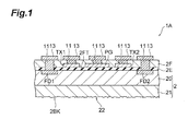
- FIG. 1 is a drawing illustrating a cross-sectional configuration of the semiconductor light detecting element according to the first embodiment.
- the semiconductor light detecting element 1A of the first embodiment functions as a range image sensor of a charge distribution method.
- the semiconductor light detecting element (range image sensor) 1A is provided with a semiconductor substrate 2, a photogate electrode PG, first and second gate electrodes TX1, TX2 (transfer electrodes), and first and second semiconductor regions FD1, FD2 (accumulation regions).
- the semiconductor substrate 2 has a light incident surface 2BK, and a front surface 2FT facing the light incident surface 2BK, or located opposite to the light incident surface 2BK.
- An insulating layer 2E is formed on the front surface 2FT of the semiconductor substrate 2.
- the semiconductor substrate 2 is comprised of silicon (Si) and the insulating layer 2E is comprised of SiO 2 .
- the semiconductor substrate 2 has a p-type (second conductivity type) epitaxial semiconductor layer 20 with a low impurity concentration on the front surface 2FT side and a semiconductor layer 21 on the light incident surface 2BK side.
- the semiconductor layer 21 has a higher impurity concentration than the epitaxial semiconductor layer 20 and in the present example it is a p-type semiconductor region.
- the light incident surface 2BK is a surface of the semiconductor layer 21 and the front surface 2FT is a surface of the epitaxial semiconductor layer 20.
- the semiconductor substrate 2 can be composed of an epitaxial substrate or an SOI epitaxial substrate, as described below.
- the photogate electrode PG is provided through the insulating layer 2E on the front surface 2FT.
- the first and second gate electrodes TX1, TX2 are provided adjacent to the photogate electrode PG and through the insulating layer 2E on the front surface 2FT.
- the first and second semiconductor regions FD1, FD2 accumulate respective charges flowing into regions immediately below the respective gate electrodes TX1, TX2.
- the photogate electrode PG has a rectangular shape on a plan view.
- the photogate electrode PG has a planar shape having first and second sides opposed to each other.
- a region corresponding to the photogate electrode PG in the semiconductor substrate 2 i.e., a region immediately below the photogate electrode PG functions as a photosensitive region in which charge is generated according to incident light.
- the photogate electrode PG is comprised of polysilicon, but it may be comprised of another material.
- the first semiconductor region FD1 is arranged on the side where the first side of the photogate electrode PG is located, and along the first side.
- the second semiconductor region FD2 is arranged on the side where the second side of the photogate electrode PG is located, and along the second side.
- the first semiconductor region FD1 and the second semiconductor region FD2 are opposed to each other with the photogate electrode PG in between in a direction in which the first and second sides are opposed to each other (which will be referred to hereinafter simply as "opposed direction").
- the first and second semiconductor regions FD1, FD2 have a rectangular shape on the plan view.
- the first and second semiconductor regions FD1, FD2 are regions of an n-type (first conductivity type) semiconductor with a high impurity concentration and are floating-diffusion regions.
- the first gate electrode TX1 is provided between the photogate electrode PG and the first semiconductor region FD1.
- the second gate electrode TX2 is provided between the photogate electrode PG and the second semiconductor region FD2.
- the first and second gate electrodes TX1, TX2 have a rectangular shape on the plan view.
- the first and second gate electrodes TX1, TX2 are comprised of polysilicon, but these may be comprised of another material.
- Epitaxial semiconductor layer 20 thickness 5-10 ⁇ m/impurity concentration 1 ⁇ 10 12 -10 15 cm -3 /resistivity 10-1000 ⁇ cm
- Semiconductor layer 21 thickness 2-10 ⁇ m/resistivity 10-20 m ⁇ cm
- First and second semiconductor regions FD1, FD2 thickness 0.1-0.4 ⁇ m/impurity concentration 1 ⁇ 10 18 -10 20 cm -3
- the insulating layer 2E there are contact holes provided for exposing surfaces of the first and second semiconductor regions FD1, FD2.
- an insulating layer 2F is formed so as to cover the photogate electrode PG and the first and second gate electrodes TX1, TX2.
- contact holes provided for exposing surfaces of the photogate electrode PG, the first and second gate electrodes TX1, TX2, and the first and second semiconductor regions FD1, FD2.
- respective contact electrodes 11 are arranged as connected to the photogate electrode PG, the first and second gate electrodes TX1, TX2, and the first and second semiconductor regions FD1, FD2, respectively.
- Pad electrodes 13 connected to the respective contact electrodes 11 are arranged each on the insulating layer 2F.
- the semiconductor light detecting element 1A is provided with the photogate electrode PG, the first and second gate electrodes TX1, TX2, the contact electrodes 11, the pad electrodes 13, etc. as conductors.
- a high-level signal e.g., a positive potential
- a high-level signal e.g., a positive potential
- gates formed by the first and second gate electrodes TX1, TX2 become open.
- Negative charge is drawn toward the first and second gate electrodes TX1, TX2 to be accumulated in potential wells formed by the first and second semiconductor regions FD1, FD2.
- An n-type semiconductor contains a positively-ionized donor, has a positive potential, and attracts electrons.
- a low-level signal e.g., the ground potential
- the gates formed by the first and second gate electrodes TX1, TX2 become closed. Charge generated in the semiconductor substrate 2 is not drawn into the first and second semiconductor regions FD1, FD2.
- the semiconductor light detecting element 1A charge generated in a deep semiconductor portion in response to incidence of light for projection is pulled into a potential well provided in the vicinity of the charge generation position on the opposite side to the light incident surface 2BK. This enables the semiconductor light detecting element 1A to perform fast and accurate ranging.
- the semiconductor substrate 2 can be formed as described below.
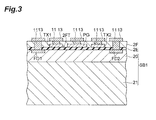
- the semiconductor substrate SB1 is a silicon substrate having the epitaxial semiconductor layer 20 and semiconductor layer 21, which is a substrate in which the epitaxial semiconductor layer 20 is grown (epitaxially grown) on the semiconductor layer 21 (which is so called an epitaxial substrate).
- the thickness of the semiconductor layer 21 in the semiconductor substrate SB1 is set to be larger than the thickness of the semiconductor layer 21 in the semiconductor light detecting element 1A.
- the thickness of the semiconductor layer 21 in the semiconductor substrate SB1 is set, for example, in the range of 400 to 700 ⁇ m.
- first and second semiconductor regions FD1, FD2, insulating layers 2E, 2F, photogate electrode PG, first and second gate electrodes TX1, TX2, contact electrodes 11, and pad electrodes 13 are formed on the prepared semiconductor substrate SB1. Since methods of forming the first and second semiconductor regions FD1, FD2, insulating layers 2E, 2F, photogate electrode PG, first and second gate electrodes TX1, TX2, contact electrodes 11, and pad electrodes 13 are well known, the description thereof is omitted herein.
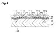
- the semiconductor substrate SB1 with the first and second semiconductor regions FD1, FD2, insulating layers 2E, 2F, photogate electrode PG, first and second gate electrodes TX1, TX2, contact electrodes 11, and pad electrodes 13 thereon is thinned.
- the semiconductor substrate SB 1 is thinned by thinning the semiconductor layer 21.
- the thinning of the semiconductor layer 21 can be performed by etching, polishing, or the like.
- the semiconductor substrate 2 can also be formed as described below.
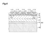
- a semiconductor substrate SB2 as base material is prepared.
- the semiconductor substrate SB2 is made using a so-called SOI (Silicon on Insulator) substrate, and is a substrate in which the epitaxial semiconductor layer 20 is grown (epitaxially grown) on the SOI substrate (which is so called an SOI epitaxial substrate).
- SOI substrate is obtained through the following process.
- a surface of a support substrate SS of Si crystal is oxidized to form an insulating layer IS of silicon oxide (SiO 2 ) on the surface of the support substrate SS.
- SiO 2 silicon oxide
- the thickness of the support substrate SS is set, for example, in the range of 400 to 700 ⁇ m.
- the insulating layer IS is set, for example, in the range of 0.3 to 0.7 ⁇ m.
- the thickness of the semiconductor substrate 21' is, for example, the same as the thickness of the semiconductor layer 21 and is set in the range of 2 to 10 ⁇ m.
- first and second semiconductor regions FD1, FD2, insulating layers 2E, 2F, photogate electrode PG, first and second gate electrodes TX1, TX2, contact electrodes 11, and pad electrodes 13 are formed on the prepared semiconductor substrate SB2. Since methods of forming the first and second semiconductor regions FD1, FD2, insulating layers 2E, 2F, photogate electrode PG, first and second gate electrodes TX1, TX2, contact electrodes 11, and pad electrodes 13 are well known, the description thereof is omitted herein.
- the semiconductor substrate SB2 with the first and second semiconductor regions FD1, FD2, insulating layers 2E, 2F, photogate electrode PG, first and second gate electrodes TX1, TX2, contact electrodes 11, and pad electrodes 13 thereon is thinned.
- the semiconductor substrate SB2 is thinned by removing the support substrate SS and insulating layer IS. This causes the semiconductor substrate 21' (semiconductor layer 21) to be exposed.
- the removal of the support substrate SS and insulating layer IS can be implemented by etching, polishing, or the like.
- Irregular asperity 22 is formed in the light incident surface 2BK of the semiconductor substrate 2 (surface of semiconductor layer 21).
- the light incident surface 2BK is optically exposed.
- the sentence "the light incident surface 2BK is optically exposed” embraces not only a state in which the light incident surface 2BK is in contact with an atmospheric gas such as air, but also a state in which an optically transparent film is formed on the light incident surface 2BK.
- the irregular asperity 22 may be formed only in a region opposed to a region immediately below each photogate electrode PG
- the irregular asperity 22 is formed, after the thinning of the semiconductor layer 21, by applying pulsed laser light to the light incident surface 2BK of the semiconductor substrate 2, i.e., to the surface of the semiconductor layer 21.
- the semiconductor substrate 2 is placed in a chamber with a gas inlet portion and a gas discharge portion and the pulsed laser light from a pulse laser generating device arranged outside the chamber is applied to the semiconductor substrate 2.
- an inert gas stream is established by guiding an inert gas (e.g., nitrogen gas, argon gas, or the like) through the gas inlet portion and discharging it through the gas discharge portion.
- an inert gas e.g., nitrogen gas, argon gas, or the like
- This setting allows dust and others made during the application of the pulsed laser light to be discharged to the outside of the chamber by the inert gas stream, thereby preventing processing debris, dust, etc. from adhering to the semiconductor substrate 2.
- the present embodiment uses a picosecond-femtosecond pulse laser generating device as the pulse laser generating device to apply picosecond-femtosecond pulsed laser light to the entire area of the light incident surface 2BK.
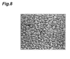
- the light incident surface 2BK is roughened by the picosecond-femtosecond pulsed laser light, whereby the irregular asperity 22 is formed in the entire area of the light incident surface 2BK, as shown in Fig. 8 .
- the irregular asperity 22 has faces intersecting with the direction perpendicular to the light incident surface 2BK (and the front surface 2FT).
- the height difference of the asperity 22 is, for example, about 0.5-10 ⁇ m and the spacing of projections in the asperity 22 is about 0.5-10 ⁇ m.
- the pulse duration of the picosecond-femtosecond pulsed laser light is, for example, about 50 fs-2 ps, the intensity, for example, about 4-16 GW, and the pulse energy, for example, about 200-800 ⁇ J/pulse. More generally, the peak intensity is 3 ⁇ 10 11 -2.5 ⁇ 10 13 (W/cm 2 ), and the fluence about 0.1-1.3 (J/cm 2 ).
- Fig. 8 is an SEM image obtained by observing the irregular asperity 22 formed in the light incident surface 2BK.
- the irregular asperity 22 is formed in the light incident surface 2BK. For this reason, light incident from the light incident surface 2BK side of the semiconductor substrate 2 into the semiconductor substrate 2 is scattered, diffused, or reflected by the asperity 22 to travel through a long distance in the semiconductor substrate 2.
- the refractive index n of Si 3.5
- the refractive index n of air 1.0.
- the semiconductor light detecting element 1A when light is incident from the direction normal to the light incident surface (light incident surface 2BK), the light is scattered or diffused by the irregular asperity 22 formed in the light incident surface 2BK, to travel in various directions.
- the light reaches the front surface 2FT light components arriving at angles of not less than 16.6° to the direction of emergence from the front surface 2FT are totally reflected by the front surface 2FT. Since light components traveling in the semiconductor substrate 2 travel in various directions because of the diffusion and the like by the asperity 22, they are extremely highly likely to be totally reflected on the front surface 2FT.
- the light components totally reflected on the front surface 2FT travel again in the semiconductor substrate 2.
- the asperity 22 Since the asperity 22 is irregularly formed, it has various angles to the direction of emergence and the totally reflected light components travel in various directions in the semiconductor substrate 2.
- the light components totally reflected on the front surface 2FT and on the light incident surface 2BK are repeatedly totally reflected on different faces so as to further increase the travel distance thereof.
- the semiconductor light detecting element 1A As the light incident into the semiconductor light detecting element 1A travels through the long distance inside the semiconductor substrate 2 as described above, it is absorbed by the semiconductor substrate 2 to generate charge. Therefore, the light incident into the semiconductor light detecting element 1A mostly travels through the long travel distance to be absorbed in the semiconductor substrate 2, without being transmitted by the semiconductor light detecting element 1A. Accordingly, the semiconductor light detecting element 1A is improved in sensitivity characteristic in the near-infrared wavelength band.
- the semiconductor substrate 2 has the semiconductor layer 21 on the light incident surface 2BK side.
- This configuration induces recombination of unnecessary carriers generated independently of light on the light incident surface 2BK side, allowing reduction in dark current.
- the semiconductor layer 21 functions as an accumulation layer to prevent charge generated by light near the light incident surface 2BK from being trapped in the light incident surface 2BK. For this reason, the charge generated by light efficiently migrates to the region immediately below the photogate electrode PG, so as to further improve the light detection sensitivity of the semiconductor light detecting element 1A.
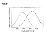
- Fig. 9 is a drawing for explaining the difference in spectral sensitivity characteristic depending upon the presence and absence of the irregular asperity.
- the spectral sensitivity characteristic of the structure with the irregular asperity 22 is indicated by a solid line and that of the structure without the irregular asperity 22 by a dashed line.
- FIG. 10 is a circuit diagram of the semiconductor light detecting element of the second embodiment.
- the semiconductor light detecting element 1B of the second embodiment functions as a semiconductor light detecting element (solid-state imaging device) of the active pixel sensor system.
- the semiconductor light detecting element 1B has a plurality of light receiving portions arrayed one-dimensionally or two-dimensionally.
- Each light receiving portion includes a photodiode PD to generate charge in a quantity according to an intensity of incident light, an amplification transistor T 1 to output a voltage value according to a quantity of charge input to a gate terminal thereof, a transfer transistor T 2 to transfer the charge generated at the photodiode PD, to the gate terminal of the amplification transistor T 1 , a discharge transistor T 3 to discharge the charge at the gate terminal of the amplification transistor T 1 , and a selection transistor T 4 to output the voltage value output from the amplification transistor T 1 , to an external line L.
- a region enclosed in a chain line corresponds to the aforementioned light receiving portion.
- the amplification transistor T 1 has a drain terminal set at a bias potential.
- the transfer transistor T 2 has a drain terminal connected to the gate terminal of the amplification transistor T 1 and a source terminal connected to a cathode terminal of the photodiode PD.
- the discharge transistor T 3 has a source terminal connected to the gate terminal of the amplification transistor T 1 and a drain terminal set at a bias potential.
- the selection transistor T 4 has a source terminal connected to a source terminal of the amplification transistor T 1 and a drain terminal connected to the line L. A constant current source is connected to the line L.
- the amplification transistor T 1 and the selection transistor T 4 constitute a source-follower circuit.
- the transfer transistor T 2 transfers the charge generated at the photodiode PD, to the gate terminal of the amplification transistor T 1 .
- a discharge control signal S reset is fed to a gate terminal of the discharge transistor T 3 and the discharge control signal S reset is at high level, the discharge transistor T 3 discharges the charge at the gate terminal of the amplification transistor T 1 ; when the transfer control signal S trans is also at high level at the same time, the discharge transistor T 3 resets the photodiode PD.
- a row selection control signal S address is fed to a gate terminal of the selection transistor T 4 and the row selection control signal S address is at high level, the selection transistor T 4 outputs the voltage value output from the amplification transistor T 1 , to the external line L.
- each light receiving portion when the transfer control signal S trans is at low level and the discharge control signal S reset is at high level, the charge at the gate terminal of the amplification transistor T 1 is discharged.
- the row selection control signal S address is at high level, the voltage value (dark signal component) output from the amplification transistor T 1 in an initialized state is output via the selection transistor T 4 to the line L.
- the discharge control signal S reset is at low level and when the transfer control signal S trans and the row selection control signal S address each are at high level, the charge generated at the photodiode PD is fed to the gate terminal of the amplification transistor T 1 . Then the voltage value (bright signal component) output from the amplification transistor T 1 according to the quantity of the charge is output via the selection transistor T 4 to the line L.
- Each of the transfer control signal S trans , the discharge control signal S reset , and the row selection control signal S address is output from an unillustrated control circuit to be fed through a line to the light receiving portion.
- Fig. 11 is a drawing illustrating a cross-sectional configuration of the semiconductor light detecting element according to the second embodiment.
- Fig. 11 shows only the photodiode PD and the transfer transistor T 2 shown in Fig. 10 , without illustration of the circuit including the other transistors T 1 , T 3 , T 4 and the various lines.
- a semiconductor substrate 3 has a p-type epitaxial semiconductor layer 30 with a low impurity concentration on the light incident surface 3FT side and a semiconductor layer 31 on the back surface 3BK side.
- the semiconductor layer 31 has a higher impurity concentration than the epitaxial semiconductor layer 30 and in the present example it is a p-type semiconductor region.
- the light incident surface 3FT is a surface of the epitaxial semiconductor layer 30 and the back surface 3BK is a surface of the semiconductor layer 31.
- the semiconductor substrate 3, as in the first embodiment can be constructed using an epitaxial substrate or an SOI epitaxial substrate.
- the light receiving portions are arrayed on the light incident surface 3FT side of the semiconductor substrate 3.
- the semiconductor substrate 3 is a silicon substrate of silicon (Si).
- Each light receiving portion is provided with an n - type first semiconductor region 33 formed in a predetermined region of the epitaxial semiconductor layer 30, a p + type second semiconductor region 34 formed on the first semiconductor region 33 and the periphery thereof, an n + type third semiconductor region 35 formed with a space relative to the first semiconductor region 33, and a gate electrode 37 provided through an insulating film 36 on the semiconductor substrate 3 and between the first semiconductor region 33 and the third semiconductor region 35.
- the first semiconductor region 33 is an n-type region with a relatively low impurity concentration.
- the second semiconductor region 34 is a p-type region with a relatively high impurity concentration.
- the third semiconductor region 35 is an n-type region with a relatively high impurity concentration.
- the phrase "relatively high impurity concentration” refers, for example, to the impurity concentration of not less than about 1 ⁇ 10 16 cm -3 , and is represented by "+” attached to conductivity type.
- the phrase “relatively low impurity concentration” refers to the impurity concentration of not more than about 1 ⁇ 10 15 cm -3 and is represented by "-" attached to conductivity type.
- the n-type impurities include antimony (Sb), arsenic (As), and so on and the p-type impurities include boron (B) and others.
- Epitaxial semiconductor layer 30 thickness 5-10 ⁇ m/impurity concentration 1 ⁇ 10 12 -10 15 cm -3 /resistivity 10-1000 ⁇ cm
- Semiconductor layer 31 thickness 2-10 ⁇ m/resistivity 10-20 m ⁇ cm
- First semiconductor region 33 thickness 0.5-3 ⁇ m/impurity concentration 1 ⁇ 10 15 -10 17 cm -3
- Second semiconductor region 34 thickness 0.1-0.3 ⁇ m/impurity concentration 1 ⁇ 10 17 -10 20 cm -3
- Third semiconductor region 35 thickness 0.1-0.5 ⁇ m/impurity concentration 1 ⁇ 10 17 -10 20 cm -3
- the epitaxial semiconductor layer 30, first semiconductor region 33, and second semiconductor region 34 constitute the photodiode PD of an embedded type.
- the epitaxial semiconductor layer 20, first semiconductor region 33, third semiconductor region 35, and gate electrode 37 constitute the transfer transistor T2 of the field effect type.
- the gate electrode 37 corresponds to the gate terminal of the transfer transistor T2, the first semiconductor region 33 to the source terminal of the transfer transistor T2, and the third semiconductor region 35 to the drain terminal of the transfer transistor T2.
- the gate electrode 37 is arranged through the insulating film 36 on the front surface side of the epitaxial semiconductor layer 20.
- the semiconductor light detecting element 1B is provided with the gate electrodes 37, electrodes for constructing the transistors T 1 , T 3 , T 4 , various lines, and others as conductors.
- the line connected to the third semiconductor region 35 is connected to the pixel circuit (other transistors T 1 , T 3 , T 4 ).
- the line connected to the gate electrode 37 is connected to an unillustrated control circuit.
- the irregular asperity 22 is formed in the back surface 3BK of the semiconductor substrate 3 (surface of semiconductor layer 31).
- the back surface 3BK is optically exposed.
- the sentence "the back surface 3BK is optically exposed” embraces not only a state in which the back surface 3BK is in contact with an atmospheric gas such as air, but also a state in which an optically transparent film is formed on the back surface 3BK.
- the irregular asperity 22 is formed by applying the pulsed laser light to the surface of the semiconductor layer 31, as described above.
- the irregular asperity 22 may be formed only in a region opposed to each photodiode PD.
- the irregular asperity 22 is formed in the back surface 3BK. For this reason, light incident through the light incident surface 3FT side of the semiconductor substrate 3 into the semiconductor substrate 3 travels inside the semiconductor substrate 3 and then is reflected, scattered, or diffused by the asperity 22 to travel through a long distance in the semiconductor substrate 3.
- light components arriving at angles of not less than 16.6° to the direction of emergence from the asperity 22 are totally reflected by the asperity 22. Since the asperity 22 is irregularly formed, it has various angles to the direction of emergence and the totally reflected light components are diffused into various directions. Therefore, the totally reflected light components include light components absorbed inside the semiconductor substrate 3 and light components arriving at the light incident surface 3FT.
- the light components arriving at the light incident surface 3FT travel in various directions because of the diffusion by the asperity 22, the light components arriving at the light incident surface 3FT are extremely highly likely to be totally reflected by the light incident surface 3FT.
- the light components totally reflected on the light incident surface 3FT are repeatedly totally reflected on different faces to further increase the travel distance thereof.
- the light incident into the semiconductor light detecting element 1B travels through the long distance inside the semiconductor substrate 3, the light is absorbed in the semiconductor substrate 3 to be detected as photocurrent.
- the semiconductor light detecting element 1B is improved in sensitivity characteristic in the near-infrared wavelength band.
- the semiconductor layer 31 induces recombination of unnecessary carriers generated independently of light on the back surface 3BK side, so as to enable reduction in dark current.
- the semiconductor layer 31 functions as an accumulation layer to prevent the charge generated by light near the back surface 3BK from being trapped in the back surface 3BK. For this reason, the charge generated by light efficiently migrates to the photodiode PD (light receiving portion), so as to further improve the light detection sensitivity of the semiconductor light detecting element 1B.
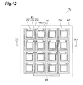
- FIG. 12 is a plan view schematically showing the semiconductor light detecting element of the third embodiment.
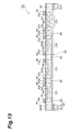
- Fig. 13 is a drawing showing a cross-sectional configuration along the line XIII-XIII of the semiconductor light detecting element shown in Fig. 12 .
- the semiconductor light detecting element 1C of the third embodiment functions as a photodiode array.
- the semiconductor light detecting element 1C is one in which a plurality of semiconductor layers and an insulating layer are laminated together on a substrate 42. As shown in Fig. 12 , the semiconductor light detecting element 1C is a multichannel avalanche photodiode array for photon counting in which a plurality of light detecting channels CH to which light to be detected is made incident are formed in a matrix (4 ⁇ 4 in the present embodiment). On the top surface side of the semiconductor light detecting element 1C there are signal conductor lines 43, resistors 44, and electrode pads 45 provided.
- the substrate 42 has, for example, a square shape about 1 mm on each side.
- Each light detecting channel CH has, for example, a square shape.
- a signal conductor line 43 consists of a readout portion 43a to transport signals output from the respective light detecting channels CH, connection portions 43b to connect the resistors 44 to the readout portion 43a, and channel peripheral portions 43c laid so as to surround the peripheries of the respective light detecting channels CH.
- the readout portion 43a is connected to each of the light detecting channels CH arranged in two columns adjacent with the readout portion 43a in between and is connected to an electrode pad 45 at one end thereof. Since in the present embodiment the photodiodes are arranged in the matrix of 4 ⁇ 4, two readout portions 43a are laid on the semiconductor light detecting element 1C. Each readout portion 43a is connected to the electrode pad 45.
- the signal conductor lines 43 are comprised, for example, of aluminum (A1).
- the resistors 44 are provided for the respective light detecting channels CH through one end portion 44a and channel peripheral portion 43c and connected through the other end portion 44b and connection portion 43b to the readout portion 43a.
- a plurality of (eight in the present embodiment) resistors 44 connected to one readout portion 43a are connected to the readout portion 43a.
- the resistors 44 are comprised, for example, of polysilicon (Poly-Si).
- the semiconductor light detecting element 1C is provided with a substrate 42, a p - type semiconductor layer 53, p + type semiconductor regions 54, a protecting film 56, a separating portion 60, and the aforementioned signal conductor lines 43 and resistors 44.
- the substrate 42 has a semiconductor layer of the n-type conductivity (first conductivity type).
- the p - type semiconductor layer 53 is formed on the substrate 42 and has the p-type conductivity (second conductivity type).
- the p + type semiconductor regions 54 are formed on the p - type semiconductor layer 53 and have the p-type conductivity.
- the separating portion 60 is formed in the p - type semiconductor layer 53 and has the n-type conductivity (first conductivity type).
- the aforementioned signal conductor lines 43 and resistors 44 are formed on the protecting film 56.
- the light to be detected is incident either from the top side or from the bottom side in Fig. 13 .
- the semiconductor light detecting element 1C is provided with the signal conductor lines 43, the resistors 44, and others as conductors.
- the substrate 42 has a substrate member SM, an insulating layer 51 formed on the substrate member SM, and an n + type semiconductor layer 52 formed on the insulating layer 51.
- the substrate member SM is comprised of Si (silicon).
- the insulating layer 51 is comprised, for example, of SiO 2 (silicon oxide).
- the n + type semiconductor layer 52 is comprised of Si and is a semiconductor layer of the n-type conductivity with a high impurity concentration.
- the thickness of the n + type semiconductor layer 52 is, for example, from 1 ⁇ m to 12 ⁇ m.
- the p - type semiconductor layer 53 is an epitaxial semiconductor layer with a low impurity concentration and of the p-type conductivity.
- the p - type semiconductor layer 53 constitutes pn junctions at interfaces to the substrate 42.
- the p - type semiconductor layer 53 has a plurality of multiplication regions AM to achieve avalanche multiplication of carriers generated with incidence of light to be detected, corresponding to the respective light detecting channels CH.
- the thickness of the p - type semiconductor layer 53 is, for example, from 3 ⁇ m to 5 ⁇ m.
- the p - type semiconductor layer 53 is comprised of Si. Therefore, the n + type semiconductor layer 52 and p - type semiconductor layer 53 constitute a semiconductor substrate (silicon substrate).
- the p + type semiconductor regions 54 are formed corresponding to the multiplication regions AM of the respective light detecting channels CH on the p - type semiconductor layer 53. Namely, regions near the interfaces to the substrate 42 of the p - type semiconductor layer 53 located below the p + type semiconductor regions 54 in the lamination direction of semiconductor layers (which will be referred to hereinafter simply as lamination direction) are the multiplication regions AM.
- the p + type semiconductor regions 54 are comprised of Si.
- the separating portion 60 is formed between the plurality of light detecting channels CH to separate the light detecting channels CH from each other. Namely, the separating portion 60 is formed so that the multiplication regions AM are formed in one-to-one correspondence to the respective light detecting channels CH in the p - type semiconductor layer 53.
- the separating portion 60 is formed in a two-dimensional grid pattern on the substrate 42 so as to completely surround the periphery of each multiplication region AM.
- the separating portion 60 is formed so as to penetrate the p - type semiconductor layer 53 from the top side to the bottom side in the lamination direction.
- the separating portion 60 contains an impurity, e.g., P and is a semiconductor layer with a high impurity concentration and of the n-type conductivity.
- the separating portion 60 may be formed by first forming trenches by etching near centers of regions corresponding to the separating portion 60 and thereafter performing the diffusion of the impurity.
- the trench grooves may be filled with a material that absorbs or reflects light in the wavelength band to be absorbed by the light detecting channels, so as to form light shield portions. In this case, it is also feasible to prevent crosstalk from occurring due to influence of emission of light by avalanche multiplication on the light detecting channels.
- the p - type semiconductor layer 53, p + type semiconductor regions 54, and separating portion 60 form a plane on the top side of the semiconductor light detecting element 1C and the protecting film 56 is formed on these.
- the protecting film 56 is formed, for example, of an insulating layer of SiO 2 .
- the signal conductor lines 43 and resistors 44 are formed on the protecting film 56.
- the readout portions 43a of the signal conductor lines 43 and the resistors 44 are formed above the separating portion 60.
- the signal conductor lines 43 function as anodes.
- a transparent electrode layer e.g., a layer of ITO (Indium Tin Oxide)
- ITO Indium Tin Oxide
- the cathode may be an electrode portion formed so as to be led to the front side.
- Fig. 14 is a drawing for schematically explaining the connection relation of each light detecting channel to the signal conductor line and resistor.
- the p + type semiconductor region 54 of each light detecting channel CH is directly connected to the signal conductor line 43 (channel peripheral portion 43c).
- This connection makes the signal conductor line 43 (channel peripheral portion 43c) and the p - type semiconductor layer 53 electrically connected.
- the p - type semiconductor layer 53 and one end portion 44a of resistor 44 are connected through the signal conductor line 43 (channel peripheral portion 43c).
- the resistor 44 has the other end portion 44b connected through the connection portion 43b to the readout portion 43a.
- the region where the plurality of light detecting channels CH are formed is thinned from the substrate member SM side so as to remove the portion corresponding to the region where the plurality of light detecting channels CH are formed in the substrate member SM.
- the substrate member SM is present as a frame portion in the periphery of the thinned region. The frame portion may also be removed whereby the substrate 42 has a configuration wherein the entire region is thinned or the entire substrate member SM is removed.
- the removal of the substrate member SM can be implemented by etching (e.g., dry etching or the like), polishing, or the like.
- the insulating layer 51 also functions as an etching stop layer. The insulating layer 51 that is exposed by removal of the substrate member SM is removed as described below.
- the irregular asperity 22 is formed in the surface of the n + type semiconductor layer 52 and throughout the entire region where the plurality of light detecting channels CH are formed.
- the region where the irregular asperity 22 is formed in the surface of the n + type semiconductor layer 52 is optically exposed.
- the sentence "the surface of the n + type semiconductor layer 52 is optically exposed” embraces not only a state in which the surface of the n + type semiconductor layer 52 is in contact with an atmospheric gas such as air, but also a state in which an optically transparent film is formed on the surface of the n + type semiconductor layer 52.
- the irregular asperity 22 may be formed only in regions opposed to the respective light detecting channels CH.
- the irregular asperity 22 is formed by applying the pulsed laser light to the insulating layer 51 exposed by removal of the substrate member SM, as in the aforementioned embodiment.
- the semiconductor light detecting element 1C When the semiconductor light detecting element 1C is used for photon counting, it is operated under an operation condition called the Geiger mode. In the Geiger-mode operation, a reverse voltage (e.g., 50 V or more) higher than the breakdown voltage is applied to each light detecting channel CH. In this state, when light to be detected is incident from the top side into each light detecting channel CH, the light to be detected is absorbed in each light detecting channel CH to generate carriers. The carriers thus generated migrate as accelerated according to an electric field in each light detecting channel CH, to be multiplied in each multiplication region AM. Then the multiplied carriers are taken through the resistor 44 to the outside by the signal conductor line 43 to be detected based on a wave height value of an output signal thereof.
- a reverse voltage e.g., 50 V or more
- the channels detecting photon provide outputs all in an identical quantity and thus a total of the outputs from all the channels is detected, thereby to count how many light detecting channels CH provided outputs in the semiconductor light detecting element 1C. Therefore, the semiconductor light detecting element 1C performs photon counting by single irradiation of light to be detected.
- the irregular asperity 22 is formed in the surface of the n + type semiconductor layer 52, the light incident into the semiconductor light detecting element 1C is reflected, scattered, or diffused by the irregular asperity 22. Therefore, the light incident into the semiconductor light detecting element 1C travels through a long distance in the semiconductor light detecting element 1C.
- the semiconductor light detecting element 1C When the semiconductor light detecting element 1C is used as a front illuminated type photodiode array, the light is incident from the protecting film 56 side into the semiconductor light detecting element 1C.
- the irregular asperity 22 formed in the surface of the n + type semiconductor layer 52, light components arriving at angles of not less than 16.6° to the direction of emergence from the irregular asperity 22 are totally reflected by the irregular asperity 22. Since the irregular asperity 22 is irregularly formed, it has various angles to the direction of emergence and the totally reflected light components diffuse into various directions. For this reason, the totally reflected light components include light components absorbed in each light detecting channel CH and light components reaching the surface on the protecting film 56 side and the side faces of the n + type semiconductor layer 52.
- the light components reaching the surface on the protecting film 56 side and the side faces of the n + type semiconductor layer 52 travel in various directions because of diffusion by the irregular asperity 22. For this reason, the light components reaching the surface on the protecting film 56 side and the side faces of the n + type semiconductor layer 52 are extremely highly likely to be totally reflected on the surface on the protecting film 56 side and the side faces of the n + type semiconductor layer 52.
- the light components totally reflected on the surface on the protecting film 56 side and the side faces of the n + type semiconductor layer 52 are repeatedly totally reflected on different faces to further increase the travel distance thereof.
- the semiconductor light detecting element 1C When the semiconductor light detecting element 1C is used as a back illuminated type photodiode array, the light is incident from the surface side of the n + type semiconductor layer 52 into the semiconductor light detecting element 1C.
- the light incident into the semiconductor light detecting element 1C is scattered by the irregular asperity 22 to travel in various directions inside the semiconductor light detecting element 1C.
- the light components reaching the surface on the protecting film 56 side and the side faces of the n + type semiconductor layer 52 travel in various directions because of diffusion by the irregular asperity 22. For this reason, the light components reaching the surface on the protecting film 56 side and the side faces of the n + type semiconductor layer 52 are extremely highly likely to be totally reflected on each face.
- the light components totally reflected on the surface on the protecting film 56 side and the side faces of the n + type semiconductor layer 52 are repeatedly totally reflected on different faces and reflected, scattered, or diffused by the irregular asperity 22, to further increase the travel distance thereof.
- the light incident into the semiconductor light detecting element 1C is reflected, scattered, or diffused by the irregular asperity 22, so as to travel through the long distance in the semiconductor light detecting element 1C, it is absorbed in each light detecting channel CH to be detected as photocurrent.
- the light incident into the semiconductor light detecting element 1C mostly travels through the long travel distance to be absorbed in each light detecting channel CH, without being transmitted by the semiconductor light detecting element 1C. Therefore, the semiconductor light detecting element 1C is improved in spectral sensitivity characteristic in the near-infrared wavelength band.
- the irregular asperity 22 is formed in the surface of the n + type semiconductor layer 52.
- This configuration induces recombination of unnecessary carriers generated independently of light on the surface side where the irregular asperity 22 is formed, so as to enable reduction in dark current.
- the n + type semiconductor layer 52 functions as an accumulation layer to prevent carriers generated by light near the surface of the n + type semiconductor layer 52, from being trapped in the surface. For this reason, the carriers generated by light efficiently migrate to the multiplication regions AM, so as to improve the light detection sensitivity of the semiconductor light detecting element 1C.
- the irregular asperity 22 is also formed in the surface corresponding to spaces between the light detecting channels CH in the n + type semiconductor layer 52 and the surface is optically exposed. For this reason, light incident into the spaces between the light detecting channels CH is also reflected, scattered, or diffused by the irregular asperity 22 to be absorbed by any one of the light detecting channels CH. Therefore, the detection sensitivity is kept from being lowered between the light detecting channels CH, thereby achieving further improvement in the light detection sensitivity of the semiconductor light detecting element 1C.
- the plurality of light detecting channels CH are formed in the third embodiment, but each light detecting channel CH is not provided for detecting the position of incidence of light and the output is the sum of outputs from the respective light detecting channels CH. For this reason, crosstalk between light detecting channels CH causes no problem and it is sufficient that the incident light is detected by any one of the light detecting channels CH.
- the pn junctions are constructed of the n + type semiconductor layer 52 in the substrate 42 and the p - type semiconductor layer 53 of the epitaxial semiconductor layer formed on the n + type semiconductor layer 52 in the substrate 42, in the semiconductor light detecting element 1C.
- the multiplication regions AM are formed in the p - type semiconductor layer 53 where the pn junctions are realized, and correspondence of each multiplication region AM to each light detecting channel CH is realized by the separating portion 60 formed between the light detecting channels CH.
- the semiconductor light detecting element 1C Since a pn junction surface is composed of the interface between the n + type semiconductor layer 52 and the p - type semiconductor layer 53 and the interface between the separating portion 60 and the p - type semiconductor layer 53, the high-concentration impurity region projects, without existence of a region including a high electric field. Therefore, the semiconductor light detecting element 1C has no ends (edges) of the pn junctions where edge breakdown can occur in the Geiger-mode operation. For this reason, there is no need for providing the pn junction of each light detecting channel CH with a guard ring in the semiconductor light detecting element 1C. This permits the semiconductor light detecting element 1C to have a considerably high aperture rate.
- the semiconductor light detecting element 1C can have higher detection efficiency. Since the light detecting channels CH are separated by the separating portion 60, it becomes feasible to suitably suppress crosstalk.
- the separating portion 60 is formed between the light detecting channels CH. For this reason, when the element is operated in the Geiger mode, even if a voltage difference becomes large between light detecting channels with incidence of photon and channels without incidence, the channels can be fully separated.
- the readout portions 43a of the signal conductor lines 43 are formed above the separating portion 60. For this reason, the signal conductor lines 43 are prevented from crossing above the multiplication regions AM, i.e., from crossing above the light detection surfaces, which further increases the aperture rate. Furthermore, it is also believed to be effective to suppression of dark current. Since in the semiconductor light detecting element 1C the resistors 44 are also formed above the separating portion 60, the aperture rate is further improved thereby.
- the inventor discovered that the problem below arises from wavelength dependence of after pulse.
- an n-type semiconductor substrate is used and a p-type epitaxial semiconductor layer is formed thereon, some of holes generated in the n-type semiconductor substrate have a delay in entering the multiplication region to cause an after pulse.
- the substrate member SM is removed from the region where the light detecting channels CH are formed, in the semiconductor light detecting element 1C, whereby the after pulse can be suppressed.
- Fig. 15 is a drawing schematically showing a cross-sectional configuration of a photodiode array according to the modification example of the layer structure of the embodiment shown in Fig. 13 .
- the fundamental planar configuration and connection relation in the modification example are the same as those shown in Fig. 12 .
- the structure shown in Fig. 15 uses an n-type semiconductor layer R53, in place of the p-type semiconductor layer 53 in Fig. 13 .
- the pn junctions are formed at interfaces between the low-concentration n-type semiconductor layer R53 and the p-type semiconductor regions 54, depletion layers spread from the pn junctions toward the n-type semiconductor layer R53, and the multiplication regions AM are formed corresponding to the depletion layers from the pn junction interfaces toward the n-type semiconductor layer R53.
- the other structure and action are the same as those described above.
- the semiconductor light detecting element 1C of the modification example is one in which a plurality of light detecting channels CH to which the light to be detected is made incident are formed in the n-type substrate 42 having the n-type semiconductor layer 52.
- the semiconductor light detecting element 1C is a photodiode array in which the plurality of light detecting channels CH to which the light to be detected is made incident are formed on the substrate with the semiconductor layer 52(S) of the first conductivity type of n + type.
- the semiconductor light detecting element 1C is provided with the substrate 42, epitaxial semiconductor layer R53, semiconductor regions 54, and resistors 44.
- the epitaxial semiconductor layer R53 is formed on the first conductivity type semiconductor layer 52 of the substrate 42 and has the first conductivity type of n - type.
- the epitaxial semiconductor layer R53 has a plurality of multiplication regions AM to achieve avalanche multiplication of carriers generated with incidence of the light to be detected, so that the multiplication regions AM correspond to the respective light detecting channels.
- the semiconductor regions 54 are formed in the first conductivity type epitaxial semiconductor layer R53 and have the second conductivity type of p + type.
- the semiconductor regions 54 make pn junctions at their interfaces to the epitaxial semiconductor layer R53.
- Each resistor 44 has two end portions and the resistors 44 are provided corresponding to the respective light detecting channels CH.
- Each resistor 44 is electrically connected through one end portion 44a to the second conductivity type semiconductor region 54 in the epitaxial semiconductor layer R53 and connected through the other end portion 44b to the signal conductor line 43.
- the resistors 44 are provided for the respective light detecting channels CH through one end portion 44a and channel peripheral portion 43c and connected through the other end portion 44b and connection portion 43b to the readout portion 43a.
- a plurality of resistors 44 to be connected to an identical readout portion 43 a are connected to the readout portion 43a.
- the pn junctions are constituted by the first conductivity type epitaxial semiconductor layer R53 on the substrate and the second conductivity type semiconductor regions 54 formed in the epitaxial semiconductor layer R53.
- the multiplication regions AM are formed in the epitaxial semiconductor layer R53 where the pn junctions are realized, and the multiplication regions AM corresponding to the respective light detecting channels are present in this epitaxial semiconductor layer R53.
- the conductivity types of p-type and n-type in the semiconductor light detecting elements 1A-1C of the embodiments may be interchanged so as to be opposite to those described above.
- the shape of the photogate electrode PG is not limited solely to the rectangular shape but may be the looped shape described in Japanese Patent Application Laid-open No. 2009-276243 .
- An optically transparent film thinner than the height difference of the asperity may be formed in the thickness of ⁇ /(4n) on the surface where the irregular asperity 22 is formed.
- This optically transparent film functions, for example, as an antireflection film to visible light.
- "n" represents the refractive index of the optically transparent film.
- the present invention can be applied to the semiconductor light detecting elements such as range image sensors, solid-state imaging devices, or avalanche photodiode arrays.
- 1A-1C...semiconductor light detecting elements 2... semiconductor substrate; 2BK...light incident surface; 2FT... front surface; 3... semiconductor substrate; 3BK...back surface; 3FT...light incident surface; 20... epitaxial semiconductor layer; 21... semiconductor layer; 22... irregular asperity; 30... epitaxial semiconductor layer; 31... semiconductor layer; 33... first semiconductor region; 34... second semiconductor region; 35...third semiconductor region; 36...insulating film; 37...gate electrode; 42... substrate; 52...n + type semiconductor layer; 53...p - type semiconductor layer; 54...p + type semiconductor region; AM... multiplication regions; FD1...first semiconductor region; FD2...second semiconductor region; PD...photodiode; PG...photogate electrode; R53... epitaxial semiconductor layer; T 1 ...amplification transistor; T 2 ...transfer transistor; T 3 ...discharge transistor; T 4 ...selection transistor; TX1... first gate electrode; TX2... second gate electrode.
Landscapes
- Solid State Image Pick-Up Elements (AREA)
- Light Receiving Elements (AREA)
- Optical Radar Systems And Details Thereof (AREA)
- Transforming Light Signals Into Electric Signals (AREA)
Applications Claiming Priority (2)
| Application Number | Priority Date | Filing Date | Title |
|---|---|---|---|
| JP2010093180A JP5726434B2 (ja) | 2010-04-14 | 2010-04-14 | 半導体光検出素子 |
| PCT/JP2011/053835 WO2011129149A1 (fr) | 2010-04-14 | 2011-02-22 | Élément semi-conducteur photo-détecteur |
Publications (3)
| Publication Number | Publication Date |
|---|---|
| EP2560215A1 true EP2560215A1 (fr) | 2013-02-20 |
| EP2560215A4 EP2560215A4 (fr) | 2014-04-09 |
| EP2560215B1 EP2560215B1 (fr) | 2018-03-28 |
Family
ID=44798528
Family Applications (1)
| Application Number | Title | Priority Date | Filing Date |
|---|---|---|---|
| EP11768670.9A Active EP2560215B1 (fr) | 2010-04-14 | 2011-02-22 | Élément semi-conducteur photo-détecteur |
Country Status (6)
| Country | Link |
|---|---|
| US (1) | US9293499B2 (fr) |
| EP (1) | EP2560215B1 (fr) |
| JP (1) | JP5726434B2 (fr) |
| KR (1) | KR101787787B1 (fr) |
| CN (1) | CN102844890B (fr) |
| WO (1) | WO2011129149A1 (fr) |
Families Citing this family (15)
| Publication number | Priority date | Publication date | Assignee | Title |
|---|---|---|---|---|
| JP2016001633A (ja) | 2014-06-11 | 2016-01-07 | ソニー株式会社 | 固体撮像素子、および電子装置 |
| JP2016062996A (ja) | 2014-09-16 | 2016-04-25 | 株式会社東芝 | 光検出器 |
| GB201421512D0 (en) * | 2014-12-03 | 2015-01-14 | Melexis Technologies Nv | A semiconductor pixel unit for simultaneously sensing visible light and near-infrared light, and a semiconductor sensor comprising same |
| EP3425683A4 (fr) | 2016-03-03 | 2019-09-25 | Hamamatsu Photonics K.K. | Élément semi-conducteur de détection de lumière |
| CN107204383B (zh) * | 2016-03-17 | 2020-02-21 | 联华电子股份有限公司 | 累崩型光检测器元件及其制作方法 |
| WO2018042785A1 (fr) * | 2016-08-29 | 2018-03-08 | 浜松ホトニクス株式会社 | Capteur de distance et capteur d'image de distance |
| JP2020009790A (ja) * | 2016-11-09 | 2020-01-16 | シャープ株式会社 | アバランシェフォトダイオード |
| JP7227802B2 (ja) * | 2019-03-15 | 2023-02-22 | 株式会社東芝 | 固体撮像装置 |
| CA3164273A1 (fr) | 2019-12-12 | 2021-06-17 | Brolis Sensor Technology, Uab | Dispositif a semi-conducteurs |
| US12451664B2 (en) | 2019-12-20 | 2025-10-21 | Nichia Corporation | Light-receiving element and light-emitting device |
| WO2021131651A1 (fr) * | 2019-12-26 | 2021-07-01 | 浜松ホトニクス株式会社 | Capteur d'image télémétrique et son procédé de fabrication |
| US12498484B2 (en) | 2019-12-26 | 2025-12-16 | Hamamatsu Photonics K.K. | Ranging image sensor |
| CN111785748A (zh) * | 2020-08-10 | 2020-10-16 | 联合微电子中心有限责任公司 | 降低背照式图像传感器暗电流的方法及结构 |
| JP7674083B2 (ja) | 2020-08-26 | 2025-05-09 | 浜松ホトニクス株式会社 | 光検出装置 |
| WO2025188695A1 (fr) * | 2024-03-07 | 2025-09-12 | Board Of Trustees Of Michigan State University | Transistors à diamant haute puissance à commande de grille électrique et optique |
Family Cites Families (24)
| Publication number | Priority date | Publication date | Assignee | Title |
|---|---|---|---|---|
| US4277793A (en) | 1979-07-16 | 1981-07-07 | Rca Corporation | Photodiode having enhanced long wavelength response |
| JP2583032B2 (ja) * | 1984-01-28 | 1997-02-19 | ローム 株式会社 | 受光素子 |
| JP2513055B2 (ja) * | 1990-02-14 | 1996-07-03 | 日本電装株式会社 | 半導体装置の製造方法 |
| JP2700356B2 (ja) | 1991-01-07 | 1998-01-21 | シャープ株式会社 | 受光素子 |
| JPH05243600A (ja) * | 1992-02-28 | 1993-09-21 | Toshiba Corp | 半導体受光素子 |
| JP3526308B2 (ja) * | 1993-02-18 | 2004-05-10 | 株式会社日立製作所 | 受光素子 |
| US5589704A (en) * | 1995-01-27 | 1996-12-31 | Lucent Technologies Inc. | Article comprising a Si-based photodetector |
| JPH0918048A (ja) * | 1995-06-28 | 1997-01-17 | Olympus Optical Co Ltd | 光電変換素子及びその製造方法 |
| JP4227069B2 (ja) | 2004-05-07 | 2009-02-18 | ローム株式会社 | 光電変換デバイス、イメージセンサおよび光電変換デバイスの製造方法 |
| ATE480009T1 (de) * | 2004-09-24 | 2010-09-15 | Harvard College | Verfahren zur herstellung von detektoren auf siliziumbasis mit lasermikrostrukturierten oberflächenschichten mit elektronendonatoren |
| US7456452B2 (en) * | 2005-12-15 | 2008-11-25 | Micron Technology, Inc. | Light sensor having undulating features for CMOS imager |
| US20070211493A1 (en) * | 2006-03-06 | 2007-09-13 | Wintek Corporation | Light guide plate with auxiliary light guide structures |
| EP3002794B1 (fr) * | 2006-07-03 | 2020-08-19 | Hamamatsu Photonics K.K. | Reseau de photodiodes |
| DE102006047706B3 (de) * | 2006-10-09 | 2008-05-29 | Terex-Demag Gmbh & Co. Kg | Nutzfahrzeug mit hydraulischer Lenkanlage |
| JP4961982B2 (ja) * | 2006-12-07 | 2012-06-27 | ソニー株式会社 | 固体撮像装置、固体撮像装置の駆動方法および撮像装置 |
| KR100850667B1 (ko) * | 2007-05-22 | 2008-08-07 | 서울옵토디바이스주식회사 | 발광 다이오드 및 그 제조방법 |
| JP4971891B2 (ja) * | 2007-07-03 | 2012-07-11 | 浜松ホトニクス株式会社 | 裏面入射型測距センサ及び測距装置 |
| EP2924465B1 (fr) | 2007-07-03 | 2017-11-29 | Hamamatsu Photonics K.K. | Capteur de mesure de distance rétroéclairé et dispositif de mesure de distance |
| JP2009047661A (ja) * | 2007-08-22 | 2009-03-05 | Hamamatsu Photonics Kk | 測距装置 |
| JP5572307B2 (ja) | 2007-12-28 | 2014-08-13 | 株式会社半導体エネルギー研究所 | 光電変換装置の製造方法 |
| JP2009218457A (ja) * | 2008-03-12 | 2009-09-24 | Panasonic Corp | 光半導体装置 |
| JP5356726B2 (ja) | 2008-05-15 | 2013-12-04 | 浜松ホトニクス株式会社 | 距離センサ及び距離画像センサ |
| JP4974183B2 (ja) | 2008-09-12 | 2012-07-11 | シャープ株式会社 | 光電変換装置 |
| JP5185207B2 (ja) * | 2009-02-24 | 2013-04-17 | 浜松ホトニクス株式会社 | フォトダイオードアレイ |
-
2010
- 2010-04-14 JP JP2010093180A patent/JP5726434B2/ja active Active
-
2011
- 2011-02-22 WO PCT/JP2011/053835 patent/WO2011129149A1/fr not_active Ceased
- 2011-02-22 KR KR1020127020749A patent/KR101787787B1/ko active Active
- 2011-02-22 CN CN201180019185.5A patent/CN102844890B/zh active Active
- 2011-02-22 EP EP11768670.9A patent/EP2560215B1/fr active Active
- 2011-02-22 US US13/634,249 patent/US9293499B2/en active Active
Also Published As
| Publication number | Publication date |
|---|---|
| KR101787787B1 (ko) | 2017-10-18 |
| JP5726434B2 (ja) | 2015-06-03 |
| EP2560215A4 (fr) | 2014-04-09 |
| EP2560215B1 (fr) | 2018-03-28 |
| US9293499B2 (en) | 2016-03-22 |
| CN102844890B (zh) | 2016-03-09 |
| CN102844890A (zh) | 2012-12-26 |
| WO2011129149A1 (fr) | 2011-10-20 |
| JP2011222893A (ja) | 2011-11-04 |
| US20130001651A1 (en) | 2013-01-03 |
| KR20130059311A (ko) | 2013-06-05 |
Similar Documents
| Publication | Publication Date | Title |
|---|---|---|
| EP2560215B1 (fr) | Élément semi-conducteur photo-détecteur | |
| US8916945B2 (en) | Semiconductor light-detecting element | |
| EP2403013B1 (fr) | Barrette de photodiodes | |
| JP5829224B2 (ja) | Mosイメージセンサ | |
| TW200822354A (en) | Photodiode array | |
| CN105810775A (zh) | 一种基于cmos图像传感器工艺的np型单光子雪崩二极管 | |
| WO2021131758A1 (fr) | Photodétecteur à semi-conducteur | |
| WO2021149650A1 (fr) | Photocapteur et système de mesure de distance | |
| US9947706B2 (en) | Semiconductor device having a light receiving element | |
| CN105895647B (zh) | 具有受光元件的光检测半导体装置 |
Legal Events
| Date | Code | Title | Description |
|---|---|---|---|
| PUAI | Public reference made under article 153(3) epc to a published international application that has entered the european phase |
Free format text: ORIGINAL CODE: 0009012 |
|
| 17P | Request for examination filed |
Effective date: 20120919 |
|
| AK | Designated contracting states |
Kind code of ref document: A1 Designated state(s): AL AT BE BG CH CY CZ DE DK EE ES FI FR GB GR HR HU IE IS IT LI LT LU LV MC MK MT NL NO PL PT RO RS SE SI SK SM TR |
|
| DAX | Request for extension of the european patent (deleted) | ||
| A4 | Supplementary search report drawn up and despatched |
Effective date: 20140306 |
|
| RIC1 | Information provided on ipc code assigned before grant |
Ipc: H04N 5/369 20110101ALI20140228BHEP Ipc: H01L 31/0236 20060101ALI20140228BHEP Ipc: H01L 27/146 20060101ALI20140228BHEP Ipc: H01L 31/10 20060101AFI20140228BHEP |
|
| GRAP | Despatch of communication of intention to grant a patent |
Free format text: ORIGINAL CODE: EPIDOSNIGR1 |
|
| STAA | Information on the status of an ep patent application or granted ep patent |
Free format text: STATUS: GRANT OF PATENT IS INTENDED |
|
| RIC1 | Information provided on ipc code assigned before grant |
Ipc: H04N 5/369 20110101ALI20171005BHEP Ipc: H01L 31/0236 20060101ALI20171005BHEP Ipc: H01L 31/10 20060101AFI20171005BHEP Ipc: H01L 27/146 20060101ALI20171005BHEP |
|
| INTG | Intention to grant announced |
Effective date: 20171026 |
|
| RIN1 | Information on inventor provided before grant (corrected) |
Inventor name: MASE, MITSUHITO Inventor name: YAMAZAKI, TOMOHIRO Inventor name: SAKAMOTO, AKIRA Inventor name: FUJII, YOSHIMARO Inventor name: SUZUKI, TAKASHI |
|
| GRAS | Grant fee paid |
Free format text: ORIGINAL CODE: EPIDOSNIGR3 |
|
| GRAA | (expected) grant |
Free format text: ORIGINAL CODE: 0009210 |
|
| STAA | Information on the status of an ep patent application or granted ep patent |
Free format text: STATUS: THE PATENT HAS BEEN GRANTED |
|
| AK | Designated contracting states |
Kind code of ref document: B1 Designated state(s): AL AT BE BG CH CY CZ DE DK EE ES FI FR GB GR HR HU IE IS IT LI LT LU LV MC MK MT NL NO PL PT RO RS SE SI SK SM TR |
|
| REG | Reference to a national code |
Ref country code: GB Ref legal event code: FG4D |
|
| REG | Reference to a national code |
Ref country code: CH Ref legal event code: EP |
|
| REG | Reference to a national code |
Ref country code: CH Ref legal event code: NV Representative=s name: SERVOPATENT GMBH, CH |
|
| REG | Reference to a national code |
Ref country code: AT Ref legal event code: REF Ref document number: 984136 Country of ref document: AT Kind code of ref document: T Effective date: 20180415 |
|
| REG | Reference to a national code |
Ref country code: IE Ref legal event code: FG4D |
|
| REG | Reference to a national code |
Ref country code: DE Ref legal event code: R096 Ref document number: 602011046939 Country of ref document: DE |
|
| PG25 | Lapsed in a contracting state [announced via postgrant information from national office to epo] |
Ref country code: LT Free format text: LAPSE BECAUSE OF FAILURE TO SUBMIT A TRANSLATION OF THE DESCRIPTION OR TO PAY THE FEE WITHIN THE PRESCRIBED TIME-LIMIT Effective date: 20180328 Ref country code: HR Free format text: LAPSE BECAUSE OF FAILURE TO SUBMIT A TRANSLATION OF THE DESCRIPTION OR TO PAY THE FEE WITHIN THE PRESCRIBED TIME-LIMIT Effective date: 20180328 Ref country code: NO Free format text: LAPSE BECAUSE OF FAILURE TO SUBMIT A TRANSLATION OF THE DESCRIPTION OR TO PAY THE FEE WITHIN THE PRESCRIBED TIME-LIMIT Effective date: 20180628 Ref country code: FI Free format text: LAPSE BECAUSE OF FAILURE TO SUBMIT A TRANSLATION OF THE DESCRIPTION OR TO PAY THE FEE WITHIN THE PRESCRIBED TIME-LIMIT Effective date: 20180328 |
|
| REG | Reference to a national code |
Ref country code: NL Ref legal event code: MP Effective date: 20180328 |
|
| REG | Reference to a national code |
Ref country code: LT Ref legal event code: MG4D |
|
| PG25 | Lapsed in a contracting state [announced via postgrant information from national office to epo] |
Ref country code: RS Free format text: LAPSE BECAUSE OF FAILURE TO SUBMIT A TRANSLATION OF THE DESCRIPTION OR TO PAY THE FEE WITHIN THE PRESCRIBED TIME-LIMIT Effective date: 20180328 Ref country code: GR Free format text: LAPSE BECAUSE OF FAILURE TO SUBMIT A TRANSLATION OF THE DESCRIPTION OR TO PAY THE FEE WITHIN THE PRESCRIBED TIME-LIMIT Effective date: 20180629 Ref country code: BG Free format text: LAPSE BECAUSE OF FAILURE TO SUBMIT A TRANSLATION OF THE DESCRIPTION OR TO PAY THE FEE WITHIN THE PRESCRIBED TIME-LIMIT Effective date: 20180628 Ref country code: LV Free format text: LAPSE BECAUSE OF FAILURE TO SUBMIT A TRANSLATION OF THE DESCRIPTION OR TO PAY THE FEE WITHIN THE PRESCRIBED TIME-LIMIT Effective date: 20180328 Ref country code: SE Free format text: LAPSE BECAUSE OF FAILURE TO SUBMIT A TRANSLATION OF THE DESCRIPTION OR TO PAY THE FEE WITHIN THE PRESCRIBED TIME-LIMIT Effective date: 20180328 |
|
| PG25 | Lapsed in a contracting state [announced via postgrant information from national office to epo] |
Ref country code: ES Free format text: LAPSE BECAUSE OF FAILURE TO SUBMIT A TRANSLATION OF THE DESCRIPTION OR TO PAY THE FEE WITHIN THE PRESCRIBED TIME-LIMIT Effective date: 20180328 Ref country code: AL Free format text: LAPSE BECAUSE OF FAILURE TO SUBMIT A TRANSLATION OF THE DESCRIPTION OR TO PAY THE FEE WITHIN THE PRESCRIBED TIME-LIMIT Effective date: 20180328 Ref country code: NL Free format text: LAPSE BECAUSE OF FAILURE TO SUBMIT A TRANSLATION OF THE DESCRIPTION OR TO PAY THE FEE WITHIN THE PRESCRIBED TIME-LIMIT Effective date: 20180328 Ref country code: EE Free format text: LAPSE BECAUSE OF FAILURE TO SUBMIT A TRANSLATION OF THE DESCRIPTION OR TO PAY THE FEE WITHIN THE PRESCRIBED TIME-LIMIT Effective date: 20180328 Ref country code: RO Free format text: LAPSE BECAUSE OF FAILURE TO SUBMIT A TRANSLATION OF THE DESCRIPTION OR TO PAY THE FEE WITHIN THE PRESCRIBED TIME-LIMIT Effective date: 20180328 Ref country code: PL Free format text: LAPSE BECAUSE OF FAILURE TO SUBMIT A TRANSLATION OF THE DESCRIPTION OR TO PAY THE FEE WITHIN THE PRESCRIBED TIME-LIMIT Effective date: 20180328 |
|
| PG25 | Lapsed in a contracting state [announced via postgrant information from national office to epo] |
Ref country code: SK Free format text: LAPSE BECAUSE OF FAILURE TO SUBMIT A TRANSLATION OF THE DESCRIPTION OR TO PAY THE FEE WITHIN THE PRESCRIBED TIME-LIMIT Effective date: 20180328 Ref country code: CZ Free format text: LAPSE BECAUSE OF FAILURE TO SUBMIT A TRANSLATION OF THE DESCRIPTION OR TO PAY THE FEE WITHIN THE PRESCRIBED TIME-LIMIT Effective date: 20180328 Ref country code: SM Free format text: LAPSE BECAUSE OF FAILURE TO SUBMIT A TRANSLATION OF THE DESCRIPTION OR TO PAY THE FEE WITHIN THE PRESCRIBED TIME-LIMIT Effective date: 20180328 |
|
| REG | Reference to a national code |
Ref country code: AT Ref legal event code: MK05 Ref document number: 984136 Country of ref document: AT Kind code of ref document: T Effective date: 20180328 |
|
| PG25 | Lapsed in a contracting state [announced via postgrant information from national office to epo] |
Ref country code: PT Free format text: LAPSE BECAUSE OF FAILURE TO SUBMIT A TRANSLATION OF THE DESCRIPTION OR TO PAY THE FEE WITHIN THE PRESCRIBED TIME-LIMIT Effective date: 20180730 |
|
| REG | Reference to a national code |
Ref country code: DE Ref legal event code: R097 Ref document number: 602011046939 Country of ref document: DE |
|
| PG25 | Lapsed in a contracting state [announced via postgrant information from national office to epo] |
Ref country code: AT Free format text: LAPSE BECAUSE OF FAILURE TO SUBMIT A TRANSLATION OF THE DESCRIPTION OR TO PAY THE FEE WITHIN THE PRESCRIBED TIME-LIMIT Effective date: 20180328 Ref country code: DK Free format text: LAPSE BECAUSE OF FAILURE TO SUBMIT A TRANSLATION OF THE DESCRIPTION OR TO PAY THE FEE WITHIN THE PRESCRIBED TIME-LIMIT Effective date: 20180328 |
|
| PLBE | No opposition filed within time limit |
Free format text: ORIGINAL CODE: 0009261 |
|
| STAA | Information on the status of an ep patent application or granted ep patent |
Free format text: STATUS: NO OPPOSITION FILED WITHIN TIME LIMIT |
|
| PG25 | Lapsed in a contracting state [announced via postgrant information from national office to epo] |
Ref country code: IT Free format text: LAPSE BECAUSE OF FAILURE TO SUBMIT A TRANSLATION OF THE DESCRIPTION OR TO PAY THE FEE WITHIN THE PRESCRIBED TIME-LIMIT Effective date: 20180328 |
|
| 26N | No opposition filed |
Effective date: 20190103 |
|
| PG25 | Lapsed in a contracting state [announced via postgrant information from national office to epo] |
Ref country code: SI Free format text: LAPSE BECAUSE OF FAILURE TO SUBMIT A TRANSLATION OF THE DESCRIPTION OR TO PAY THE FEE WITHIN THE PRESCRIBED TIME-LIMIT Effective date: 20180328 |
|
| PG25 | Lapsed in a contracting state [announced via postgrant information from national office to epo] |
Ref country code: LU Free format text: LAPSE BECAUSE OF NON-PAYMENT OF DUE FEES Effective date: 20190222 Ref country code: MC Free format text: LAPSE BECAUSE OF FAILURE TO SUBMIT A TRANSLATION OF THE DESCRIPTION OR TO PAY THE FEE WITHIN THE PRESCRIBED TIME-LIMIT Effective date: 20180328 |
|
| REG | Reference to a national code |
Ref country code: BE Ref legal event code: MM Effective date: 20190228 |
|
| REG | Reference to a national code |
Ref country code: IE Ref legal event code: MM4A |
|
| PG25 | Lapsed in a contracting state [announced via postgrant information from national office to epo] |
Ref country code: IE Free format text: LAPSE BECAUSE OF NON-PAYMENT OF DUE FEES Effective date: 20190222 |
|
| PG25 | Lapsed in a contracting state [announced via postgrant information from national office to epo] |
Ref country code: BE Free format text: LAPSE BECAUSE OF NON-PAYMENT OF DUE FEES Effective date: 20190228 |
|
| PG25 | Lapsed in a contracting state [announced via postgrant information from national office to epo] |
Ref country code: TR Free format text: LAPSE BECAUSE OF FAILURE TO SUBMIT A TRANSLATION OF THE DESCRIPTION OR TO PAY THE FEE WITHIN THE PRESCRIBED TIME-LIMIT Effective date: 20180328 |
|
| REG | Reference to a national code |
Ref country code: CH Ref legal event code: PCAR Free format text: NEW ADDRESS: WANNERSTRASSE 9/1, 8045 ZUERICH (CH) |
|
| PG25 | Lapsed in a contracting state [announced via postgrant information from national office to epo] |
Ref country code: MT Free format text: LAPSE BECAUSE OF NON-PAYMENT OF DUE FEES Effective date: 20190222 |
|
| PG25 | Lapsed in a contracting state [announced via postgrant information from national office to epo] |
Ref country code: CY Free format text: LAPSE BECAUSE OF FAILURE TO SUBMIT A TRANSLATION OF THE DESCRIPTION OR TO PAY THE FEE WITHIN THE PRESCRIBED TIME-LIMIT Effective date: 20180328 |
|
| PG25 | Lapsed in a contracting state [announced via postgrant information from national office to epo] |
Ref country code: IS Free format text: LAPSE BECAUSE OF FAILURE TO SUBMIT A TRANSLATION OF THE DESCRIPTION OR TO PAY THE FEE WITHIN THE PRESCRIBED TIME-LIMIT Effective date: 20180728 |
|
| PG25 | Lapsed in a contracting state [announced via postgrant information from national office to epo] |
Ref country code: HU Free format text: LAPSE BECAUSE OF FAILURE TO SUBMIT A TRANSLATION OF THE DESCRIPTION OR TO PAY THE FEE WITHIN THE PRESCRIBED TIME-LIMIT; INVALID AB INITIO Effective date: 20110222 |
|
| REG | Reference to a national code |
Ref country code: DE Ref legal event code: R081 Ref document number: 602011046939 Country of ref document: DE Owner name: SIONYX, LLC, BEVERLY, US Free format text: FORMER OWNER: HAMAMATSU PHOTONICS K.K., HAMAMATSU-SHI, SHIZUOKA, JP |
|
| REG | Reference to a national code |
Ref country code: GB Ref legal event code: 732E Free format text: REGISTERED BETWEEN 20220113 AND 20220119 |
|
| PG25 | Lapsed in a contracting state [announced via postgrant information from national office to epo] |
Ref country code: MK Free format text: LAPSE BECAUSE OF FAILURE TO SUBMIT A TRANSLATION OF THE DESCRIPTION OR TO PAY THE FEE WITHIN THE PRESCRIBED TIME-LIMIT Effective date: 20180328 |
|
| REG | Reference to a national code |
Ref country code: DE Ref legal event code: R119 Ref document number: 602011046939 Country of ref document: DE |
|
| REG | Reference to a national code |
Ref country code: CH Ref legal event code: PL |
|
| GBPC | Gb: european patent ceased through non-payment of renewal fee |
Effective date: 20220222 |
|
| REG | Reference to a national code |
Ref country code: DE Ref legal event code: R073 Ref document number: 602011046939 Country of ref document: DE |
|
| REG | Reference to a national code |
Ref country code: DE Ref legal event code: R074 Ref document number: 602011046939 Country of ref document: DE |
|
| REG | Reference to a national code |
Ref country code: GB Ref legal event code: S28 Free format text: APPLICATION FILED |
|
| PG25 | Lapsed in a contracting state [announced via postgrant information from national office to epo] |
Ref country code: FR Free format text: LAPSE BECAUSE OF NON-PAYMENT OF DUE FEES Effective date: 20220228 |
|
| REG | Reference to a national code |
Ref country code: GB Ref legal event code: S28 Free format text: RESTORATION ALLOWED Effective date: 20221208 |
|
| PG25 | Lapsed in a contracting state [announced via postgrant information from national office to epo] |
Ref country code: GB Free format text: LAPSE BECAUSE OF NON-PAYMENT OF DUE FEES Effective date: 20220222 Ref country code: FR Free format text: LAPSE BECAUSE OF NON-PAYMENT OF DUE FEES Effective date: 20220228 |
|
| PGRI | Patent reinstated in contracting state [announced from national office to epo] |
Ref country code: FR Effective date: 20221124 |
|
| P01 | Opt-out of the competence of the unified patent court (upc) registered |
Effective date: 20230530 |
|
| REG | Reference to a national code |
Ref country code: DE Ref legal event code: R079 Ref document number: 602011046939 Country of ref document: DE Free format text: PREVIOUS MAIN CLASS: H01L0031100000 Ipc: H10F0030200000 |
|
| REG | Reference to a national code |
Ref country code: CH Ref legal event code: U11 Free format text: ST27 STATUS EVENT CODE: U-0-0-U10-U11 (AS PROVIDED BY THE NATIONAL OFFICE) Effective date: 20260301 |
|
| PGFP | Annual fee paid to national office [announced via postgrant information from national office to epo] |
Ref country code: GB Payment date: 20260219 Year of fee payment: 16 |
|
| PGFP | Annual fee paid to national office [announced via postgrant information from national office to epo] |
Ref country code: DE Payment date: 20260219 Year of fee payment: 16 |
|
| PGFP | Annual fee paid to national office [announced via postgrant information from national office to epo] |
Ref country code: FR Payment date: 20260219 Year of fee payment: 16 |
|
| PGFP | Annual fee paid to national office [announced via postgrant information from national office to epo] |
Ref country code: CH Payment date: 20260301 Year of fee payment: 16 |