EP2562930B1 - Verstärker der Klasse D und Steuerverfahren - Google Patents
Verstärker der Klasse D und Steuerverfahren Download PDFInfo
- Publication number
- EP2562930B1 EP2562930B1 EP11178895.6A EP11178895A EP2562930B1 EP 2562930 B1 EP2562930 B1 EP 2562930B1 EP 11178895 A EP11178895 A EP 11178895A EP 2562930 B1 EP2562930 B1 EP 2562930B1
- Authority
- EP
- European Patent Office
- Prior art keywords
- output
- bridge
- amplifier
- state
- switching
- Prior art date
- Legal status (The legal status is an assumption and is not a legal conclusion. Google has not performed a legal analysis and makes no representation as to the accuracy of the status listed.)
- Active
Links
Images


Classifications
-
- H—ELECTRICITY
- H03—ELECTRONIC CIRCUITRY
- H03F—AMPLIFIERS
- H03F3/00—Amplifiers with only discharge tubes or only semiconductor devices as amplifying elements
- H03F3/20—Power amplifiers, e.g. Class B amplifiers, Class C amplifiers
- H03F3/21—Power amplifiers, e.g. Class B amplifiers, Class C amplifiers with semiconductor devices only
- H03F3/217—Class D power amplifiers; Switching amplifiers
- H03F3/2173—Class D power amplifiers; Switching amplifiers of the bridge type
-
- H—ELECTRICITY
- H03—ELECTRONIC CIRCUITRY
- H03F—AMPLIFIERS
- H03F1/00—Details of amplifiers with only discharge tubes, only semiconductor devices or only unspecified devices as amplifying elements
- H03F1/52—Circuit arrangements for protecting such amplifiers
Definitions
- This invention relates to class D amplifiers, and relates to the prevention of coincidental high current switching in Class-D amplifiers.
- Class-D amplifiers are commonly used as speaker drivers in consumer, automotive and mobile applications. See, for example, US 2007/0236286 , US 2009/0097178 , and US 2001/0010482 .
- Class-D amplifiers are switch-mode amplifiers meaning the output node(s) are switched between the supply rails usually employing some form of pulse-width modulation (PWM). Because the power transistors are either fully on or fully off for most of the time, this results in high efficiency that is the defining feature of class-D amplifiers.
- PWM pulse-width modulation
- a less attractive side effect of switch mode operation is the occurrence of high current transients in the supply and ground rails. In combination with parasitic inductance in the supply and ground lines these current transients cause significant voltage excursions at the supply and ground terminals of a class-D output stage.
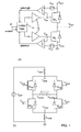
- FIG. 1 (a) A simplified schematic of a typical class-D half-bridge output stage is shown in Figure 1 (a) . It consists of a very large PMOS transistor (M H ) connected between the supply line V SUP and the output node, and a very large NMOS power transistor (M L ) connected between the ground line V GND and the output node. Note that a configuration with only NMOS transistors is also possible.
- M H PMOS transistor
- M L very large NMOS power transistor
- a control logic block 10 controls the gate drivers 12 of the power transistors M H , M L using the input signal “in” and the “gatehigh” and “gatelow” signals.
- the "gatehigh” and “gatelow” signal or similar signals are generally available in class-D output stages to implement a break-before-make mechanism.
- Figure 1 (a) also shows an input signal "enable” to the control logic 10. This is a signal which is pulled low to implement shut down of the amplifier.
- Bridge-Tied-Load (BTL) configuration consists of two complementary half-bridges as shown in Figure 1 (b) .
- One half-bridge A has high and low transistors M HA , M LA and the other half-bridge B has high and low transistors M HB , M LB .
- Each half-bridge has comparators for deriving the "gatehigh” and “gatelow” logic signals, as well as control logic, but these are not shown in order to simplify Figure 1 (b) .
- the output load (for example a loudspeaker as shown) is connected between the output nodes V OUTA and V OUTB of the two half-bridges.
- the loudspeaker can be modelled as a series connection of a resistor and an inductor, e.g. 8 ⁇ /68 ⁇ H, 4 ⁇ /33 ⁇ H.
- the half-bridges in a BTL power stage share the same supply and ground pins and thus also the same parasitic conductance between the on-chip ground and supply nets and the external ground and supply. These parasitic inductances are the result of bonding wires and PCB tracks.
- the lowside power transistor M LA is opened and subsequently highside power transistor M HA is closed causing a rising edge at node V OUTA . Consequently, the current is now forced to flow in a loop as shown in Figure 2(b) and the current that was flowing through the parasitic inductances L SUP and L GND drops to zero. This sudden current drop causes a positive voltage excursion on internal supply node V SUPi and a negative voltage excursion on internal node V GNDi . The magnitude of these voltage excursions depends on the value of the parasitic inductances and the rate of change of the current.
- Figure 3(a) the simulated voltage transients on the output nodes V OUTA and V OUTB and the internal supply and ground nets V SUPi and V GNDi are shown.
- L SUP and L GND a value of 1nH has been used and the external supply voltage is 5V.
- Figure 3 shows the voltage transients for non coinciding edges ( Figure 3(a) ) and for coinciding edges ( Figure 3(b) ).
- the large voltage overshoots seen by the power transistors are a robustness hazard.
- Especially the NMOS transistors are vulnerable because they typically exhibit a destructive bipolar mode that is triggered when the drain-source voltage exceeds a critical value.
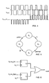
- ternary or BD-modulation is widely preferred because it allows for filterless application.
- the output signals V OUTA and V OUTB are switching synchronously with 50% duty-cycle. In this case the differential signal across the loudspeaker and therefore also the output current is zero.
- the duty-cycles of V OUTA and V OUTB change in opposite direction, e.g. if the duty-cycle of V OUTA increases then the duty-cycle of V OUTB decreases and vice versa. This results in a three level differential signal across the load as shown in Figure 4 , which shows the BD-modulation.
- the critical condition described earlier where opposite output transitions coincide, appears to be avoided.
- the first exception that will be called the overcurrent coincidence, occurs when the current through one of the power transistors crosses a limit current.
- the output stage is equipped with an overcurrent protection that prevents damage in case of short-circuits. If the overcurrent protection is triggered the corresponding power transistor is switched off immediately to prevent a further increase in current. If this event coincides with an output transition of the opposite half-bridge this creates exactly the critical condition described earlier.
- the second exception that will be called the shutdown coincidence, occurs when the amplifier is switched off. In this case all power transistors are switched off simultaneously and if at that moment the output current is large this also creates exactly the critical condition described earlier. Both these mechanisms have been observed in practice to be the cause of robustness problems in class-D amplifiers.
- a Class D power amplifier for driving a load between first and second output nodes, comprising:
- the latches enable the overcurrent detection signals to be short pulses.
- the controllers can be further adapted to:
- the controllers can be further adapted, in response to a signal to shut down the amplifier, to delay shutdown of one output half-bridge with respect to the other half-bridge only if one half-bridge output is high and the other is low.
- a shut down signal for each output half-bridge can be delayed only if the half-bridge output has predetermined value, and the predetermined value is the same for the two output half-bridges. This means no communication is needed between the half-bridges - the delay is implemented simply based on the output of the same output half-bridge.
- An asynchronous logic circuit can be used to implement the delay.
- the amplifier of the invention can be used as the output stage of a DC-DC boost converter.
- a logic circuit can then be used for generating a boost stage hold signal based on the state of the amplifier output half-bridges, such that switching of the boost stage is prevented when switching of the amplifier is taking place.
- a Class D power amplifier which drives a load between first and second output nodes, the amplifier comprising:
- the invention provides a Class D power amplifier for driving a load between first and second output nodes defined between two half-bridges.
- a controller is adapted to derive an amplifier hold signal when an overcurrent state is detected in that output half-bridge, and this hold signal is used to prevent switching of the other output half-bridge between the two main output states.
- the invention is based on the recognition that to avoid an overcurrent coincidence the bridge-halves need to be aware if the other bridge-half is in the middle of or starting a transition.
- a signal can be generated that flags the start and finish of each transition. This signal can be easily generated since the sequence of events during a transition is fixed. For example during a falling transition the following sequence of events occurs:
- the signal "gatehigh” goes high. This marks the end of the transition and the state-machine jumps to state S 2 .
- the transition starts when the state-machine jumps to state S 3 after a falling edge of input signal "in”.
- the invention aims to prevent overcurrent coincidence, and this is achieved in that an overcurrent protection mode is triggered.
- two logic signals "oc_high” and “oc_low” are introduced that flag the occurrence of an overcurrent in the highside power transistor or lowside power transistor respectively.
- the "oc_high” and “oc_low” signal or similar signals are generally available in class-D output stages as explained in more detail in Berkhout, M., "Integrated Overcurrent Protection System for Class-D Audio Power Amplifiers", IEEE Journal of Solid-State Circuits, vol.40, no.11, pp. 2237-2245, 2005 .
- Overcurrent protection is used to ensure that the power transistors operate in their safe operating area (SOA).
- SOA safe operating area
- the SOA can be defined as a current limit.
- the current through the power transistors can be measured by placing low-ohmic resistors in series between the power lines and the power transistors, and measuring the voltage drops.
- the current can be determined by comparing the drain to source voltage of each power transistor with a reference transistor through which a reference current is known to flow.
- the article "Integrated Overcurrent Protection System for Class-D Audio Power Amplifiers" referenced above presents an approach in which overcurrent logic is additionally used to process the control signals before application to the control logic.
- the overcurrent detection signals to be used in the amplifier of the invention can be of any type, including the basic voltage drop measurement approach as well as the more complicated approaches explained in "Integrated Overcurrent Protection System for Class-D Audio Power Amplifiers".
- the invention makes use of a logic signal which will be termed "hold", that goes high when an overcurrent occurs in one half-bridge. This is used to avoid switching coincidence by preventing the other half-bridge from switching.
- the required "hold” signal can be derived easily from the available signals, for example using a logic circuit, for example as shown in Figure 6 .
- the circuit comprises two set-reset latches and an OR gate.
- the Set input to each latch is a logic AND signal which requires the state machine to be in the correct state and the overcurrent signal to be present in the transistor that is turned on for that state - one latch is triggered (to the Set input) by the state machine being in the low output state S 0 and the "oc_low” signal is received, and the other is triggered by the state machine being in the high output state S 2 and the "oc_high” signal is received. If either of these overcurrent signals is received, a hold signal is generated by the OR logic.
- the latches are needed because the "oc_low” or “oc_high” flag goes low as soon as the corresponding power transistor is switched off, i.e. during the transition, so that a Reset is only provided at the next output state.
- control of the state in which the circuit is operating is by the control logic, which generates the required timing signals for controlling the power transistor gates.
- state S 0 or state S 2 The transition out of state S 0 or state S 2 is only allowed if the hold signal is low.
- state S 3 which is the transition from high (S 2 ) to low (S 0 )
- the transitions from state S 0 to S 1 and from S 2 to S 3 are blocked when the hold signal is high. Furthermore, if the state-machine is in state S 1 , i.e. after the output transition has already started, it can revert back to state S 0 as long as the "gatelow” signal is high, i.e. as long as the lowside gate is not fully discharged. This is similar to the reversal from state S 3 and the "gatehigh" signal as explained above.
- the modified state-machine and hold signal generation are implemented in both bridge-halves such that the hold signal from bridge-half A taps into the state-machine of half-bridge B and vice versa.
- a very simple solution is to delay shutdown of a half-bridge only when the instantaneous output is high. If the instantaneous output is low then no delay is applied. In this way, both bridge halves shut down at the same time when they are switching in-phase. Only if the outputs of the bridge-halves are not equal the shutdown of one bridge-half is delayed. The delay can be quite small, e.g. in the order of 20ns.
- This approach does not require any communication between half-bridges. It implements a delay in both half-bridges if the outputs are both high, and no delay in both half-bridges if the outputs are both low. Of course, the delay could instead only be when the instantaneous output is low.
- Figure 8 shows a very simple logic circuit that applies a delay to the falling edge of an enable signal only if the output is high.
- the resulting signal (“enable_out”) can comprise the “enable” signal applied to the control logic as shown in Figure 1(a) , and the falling edge corresponds to a shut down command.
- the "enable” signal is low, both power transistors are switched off leaving the output node in a high-impedance state.
- the "enable” signal is high, the output node switches normally, according to the value of input signal "in”.
- an enable signal “enable_in” is delayed by a delay element before being combined with AND logic with the output signal "out”.
- the circuit of Figure 8 is inserted between the "enable” input to the control logic and the control logic for each of the half-bridges.
- the enable_out signal of Figure 8 is applied as the "enable” signal to the control logic as shown in Figure 1(a) .
- the output stage is exactly as shown in Figure 1 (b) .
- This example of DC-DC boost converter consists of a large NMOS and PMOS power transistor M LC and M HC , an external- inductor L BST and an external capacitor C BST . It boosts the supply voltage V SUP to a higher value V BST . In order to do so, the power transistors M LC and M HC switch the input node V IN up and down between the output V BST and ground.
- the current through inductor L BST can be considered constant during transitions of V IN and is switched between ground and V BST . Similar to the class-D power stage this causes large and fast changes in the current that in turn yield large voltage excursions across the parasitic inductances in the current loops.
- the DC-DC booster output voltage V BST and the class-D supply voltage are connected off-chip to the booster capacitor C BST .
- Typical values for L BST and C BST in mobile applications are 1 ⁇ H and 10 ⁇ F respectively.
- the DC-DC boost converter needs to switch very fast, e.g. 2 MHz which is 5 to 6 times faster than the class-D amplifier.
- the booster when the booster is active the current is certainly high or it would make no sense to use the booster in the first place. Again it makes sense to avoid coincidental switching of the power stages to prevent addition of voltage excursions.
- the circuit shown in Figure 10 generates a signal hold_bst that indicates that one or both bridge-halves of the class-D amplifier are in transition.
- the signal "hold_bst” is then tapped into the control state-machine of the DC-DC boost converter similar to that shown in Figure 7 .
- the "hold_bst" signal is generated by the amplifier half-bridges and only stops (or actually delays) the switching of the boost converter half-bridge.
- the boost converter half-bridge has no influence on the switching of the amplifier half-bridges. The result is that the boost converter only switches when the amplifier is not switching.
- the control logic for all three half-bridges is the same and is described by the state-diagram in Figure 7 .
- the "hold_bst" signal is based on the current states of the amplifier half-bridges. For each half-bridge, an output signal is generated when the intermediate states S 1 or S 3 are entered. The output state is reset when the states S 2 or S 0 are entered. Thus, the hold signal is applied to the DC-DC boost converter when the amplifier is switching between the output states S 0 and S 2 .
- the invention can be realised as logic functions that can be implemented using standard CMOS or any other type of logic.
- the invention can be used in class-D audio amplifiers, DC-DC converters and combinations of both.
Landscapes
- Engineering & Computer Science (AREA)
- Power Engineering (AREA)
- Amplifiers (AREA)
Claims (11)
- Ein Klasse D Leistungsverstärker zum Lenken einer Ladung zwischen einem ersten und einem zweiten Ausgabeknoten, aufweisend:eine erste Ausgabe-Halbbrücke aufweisend einen ersten highside und einen zweiten lowside Transistor (MHA, MLA) in Reihe zwischen Stromschienen, mit dem ersten Ausgabeknoten (VOUTA) zwischen dem ersten und dem zweiten Transistor;eine zweite Ausgabe-Halbbrücke aufweisend einen dritten highside und einen vierten lowside Transistor (MHB, MLB) in Reihe zwischen Stromschienen, mit dem zweiten Ausgabeknoten (VOUTB) zwischen dem dritten und dem vierten Transistor;einen ersten Controller von der ersten Ausgabe-Halbbrücke zum Generieren von Gate-Treibersignalen für den highside und den lowside Transistor in der ersten Ausgabe-Halbbrücke; undeinen zweiten Controller von der zweiten Ausgabe-Halbbrücke zum Generieren von Gate-Treibersignalen für den highside und den lowside Transistor in der zweiten Ausgabe-Halbbrücke;wobei die Controller eingerichtet sind zum Ableiten eines Verstärker-Haltesignals (hold), wenn ein Überstrom-Status in einer Ausgabe-Halbbrücke detektiert ist, und um ein Umschalten von der anderen Ausgabe-Halbbrücke basierend auf dem Haltesignal zu verhindern, undwobei die Controller jeweils einen asynchronen Logikschaltkreis aufweisen zum Generieren des Verstärker-Haltesignals, wobei der asynchrone Logikschaltkreis, für jede Ausgabe-Halbbrücke, aufweist
ein erstes Latch zum Generieren einer ersten Ausgabe, wenn ein Überstrom in dem lowside Transistor detektiert ist und der Ausgabestatus von dem Verstärker ein erster Status (S0) ist, in welchem die Halbbrücke ihren Ausgabeknoten herunter zieht, und
ein zweites Latch zum Generieren einer zweiten Ausgabe, wenn ein Überstrom in dem highside Transistor detektiert ist und der Ausgabestatus von der Halbbrücke ein zweiter Status (S2) ist, in welchem die Halbbrücke ihren Ausgabeknoten heraufzieht, wobei ein Ausgabe-Halbbrücken Haltesignal (hold) das logische ODER von der ersten und der zweiten Ausgabe aufweist. - Ein Verstärker gemäß Anspruch 1, wobei die Controller ferner eingerichtet sind zum:Verwenden des Verstärker-Haltesignals (hold), um ein Umschalten von der anderen Ausgabe-Halbbrücke aus dem ersten und dem zweiten Ausgabestatus (So, S2) heraus zu verhindern, wenn das Umschalten nicht begonnen hat; undZurückbringen der anderen Ausgabe-Halbbrücke zu dem ersten oder dem zweiten Ausgabestatus (So, S2), wenn das Umschalten aus dem Status heraus begonnen hat, aber ein Ausschalten von einem Transistor nicht fertiggestellt wurde.
- Ein Verstärker gemäß einem der vorhergehenden Ansprüche, wobei die Controller ferner eingerichtet sind, als Erwiderung auf ein Signal (enable) den Verstärker abzuschalten, um
ein Abschalten von einer Ausgabe-Halbbrücke in Bezug auf die andere Halbbrücke nur zu verzögern, wenn eine Halbbrücken-Ausgabe hoch ist und die Andere niedrig ist. - Ein Verstärker gemäß Anspruch 3, wobei jeder Controller aufweist einen asynchronen Logikschaltkreis, um ein Ausschaltsignal für die entsprechenden Ausgabe-Halbbrücken nur dann zu verzögern, wenn die Halbbrücken-Ausgabe einen vorbestimmten Wert hat, und wobei der vorbestimmte Wert derselbe ist für die zwei Ausgabe-Halbbrücken.
- Ein DC-DC Boostwandler aufweisend eine DC-DC Booststufe (MHC, MLC) und einen Verstärker gemäß einem der vorhergehenden Ansprüche.
- Ein Stoßwandler gemäß Anspruch 5, aufweisend einen Logikschaltkreis zum Generieren eines Booststufen Haltesignals basierend auf dem Status von den Verstärker-Ausgabe-Halbbrücken, so dass ein Umschalten von der Stoßstufe verhindert ist, wenn ein Umschalten von dem Verstärker stattfindet.
- Ein Verfahren zum Steuern eines Klasse D Leistungsverstärkers, welcher eine Ladung zwischen einem ersten und einem zweiten Ausgabeknoten lenkt, der Verstärker aufweisend:eine erste Ausgabe-Halbbrücke aufweisend einen ersten highside und einen zweiten lowside Transistor (MHA, MLA) in Reihe zwischen Stromschienen, mit dem ersten Ausgabeknoten (VOUTA) zwischen dem ersten und dem zweiten Transistor; undeine zweite Ausgabe-Halbbrücke aufweisend einen dritten highside und einen vierten lowside Transistor (MHB, MLB) in Reihe zwischen Stromschienen, mit dem zweiten Ausgabeknoten (VOUTB) zwischen dem dritten und dem vierten Transistor, wobei das Verfahren aufweist:für jede Ausgabe-Halbbrücke, Steuern der Ausgabe-Halbbrücke, um einen ersten Ausgabestatus (S0) zu bestimmen, in welchem die Ausgabe-Halbbrücke den Ausgabeknoten zu der niedrigen Stromschiene herunter zieht, und einen zweiten Ausgabestatus (S2), in welchem die Ausgabe-Halbbrücke den Ausgabeknoten zu der hohen Stromschiene herauf zieht;Ableiten eines Verstärker-Haltesignals (hold), wenn ein Überstrom-Status in einer Halbbrücke detektiert wird, und Verwenden des Haltesignals, um ein Umschalten von der anderen Ausgabe-Halbbrücke zwischen dem ersten und dem zweiten Ausgabestatus (So, S2) zu verhindern, und ferner aufweisend,für jede Ausgabe-Halbbrücke,
Generieren einer ersten Ausgabe von einem Latch, wenn ein Überstrom in dem lowside Transistor detektiert wird und der Ausgabestatus von dem Verstärker derjenige ist, in welchem die Halbbrücke ihren Ausgabeknoten herunter zieht, und
Generieren einer zweiten Ausgabe von einem Latch, wenn ein Überstrom in dem highside Transistor detektiert wird und der Ausgabestatus von dem Verstärker derjenige ist, in welchem die Halbbrücke ihren Ausgabeknoten heraufzieht,
wobei das Verfahren aufweist
Generieren eines Ausgabe-Halbbrücken Haltesignals (hold) als das logische ODER von der ersten und der zweiten Ausgabe. - Ein Verfahren gemäß Anspruch 7, aufweisend:Verwenden des Verstärker-Haltesignals, um Umschalten von der anderen Ausgabe-Halbbrücke aus dem ersten und dem zweiten Ausgabestatus heraus zu verhindern, wenn das Umschalten nicht begonnen hat; undZurückbringen der anderen Ausgabebrücke von dem ersten oder dem zweiten Ausgabestatus, wenn das Umschalten aus dem Status heraus begonnen hat, aber ein Ausschalten von einem Transistor nicht fertiggestellt wurde.
- Ein Verfahren gemäß einem der Ansprüche 7 oder 8, aufweisend, als Erwiderung auf ein Signal den Verstärker auszuschalten, Verzögern eines Abschaltens von einer Ausgabe-Halbbrücke in Bezug zu der anderen Ausgabe-Halbbrücke, wenn eine Ausgabe-Halbbrücken Ausgabe hoch und die andere niedrig ist.
- Ein Verfahren gemäß Anspruch 9, aufweisend Verzögern eines Ausschalt-Signals für die jeweilige Ausgabe-Halbbrücke nur dann, wenn die Ausgabe-Halbbrücken-Ausgabe einen vorbestimmten Wert hat, und wobei der vorbestimmte Wert derselbe für die zwei Ausgabe-Halbbrücken ist.
- Ein Verfahren gemäß einem der Ansprüche 7 bis 10, wobei das Verfahren zum Steuern eines Verstärkers an dem Ausgang von einem DC-DC Boostwandler ist, wobei das Verfahren ferner aufweist
Generieren eines Booststufen Haltesignals basierend auf dem Status von den Verstärker Ausgabe-Halbbrücken, und
Verwenden des Booststufen Haltesignals, um ein Umschalten von der Stoßstufe zu verhindern, wenn ein Umschalten von dem Verstärker stattfindet.
Priority Applications (3)
| Application Number | Priority Date | Filing Date | Title |
|---|---|---|---|
| EP11178895.6A EP2562930B1 (de) | 2011-08-25 | 2011-08-25 | Verstärker der Klasse D und Steuerverfahren |
| CN201210303461.7A CN102957383B (zh) | 2011-08-25 | 2012-08-23 | D类放大器和控制方法 |
| US13/593,231 US9160290B2 (en) | 2011-08-25 | 2012-08-23 | Class D amplifier and control method |
Applications Claiming Priority (1)
| Application Number | Priority Date | Filing Date | Title |
|---|---|---|---|
| EP11178895.6A EP2562930B1 (de) | 2011-08-25 | 2011-08-25 | Verstärker der Klasse D und Steuerverfahren |
Publications (2)
| Publication Number | Publication Date |
|---|---|
| EP2562930A1 EP2562930A1 (de) | 2013-02-27 |
| EP2562930B1 true EP2562930B1 (de) | 2015-04-01 |
Family
ID=44785267
Family Applications (1)
| Application Number | Title | Priority Date | Filing Date |
|---|---|---|---|
| EP11178895.6A Active EP2562930B1 (de) | 2011-08-25 | 2011-08-25 | Verstärker der Klasse D und Steuerverfahren |
Country Status (3)
| Country | Link |
|---|---|
| US (1) | US9160290B2 (de) |
| EP (1) | EP2562930B1 (de) |
| CN (1) | CN102957383B (de) |
Families Citing this family (8)
| Publication number | Priority date | Publication date | Assignee | Title |
|---|---|---|---|---|
| EP2495875A4 (de) * | 2009-10-26 | 2013-12-18 | Nissan Motor | Treiberschaltung für ein schaltelement und stromumrichter damit |
| JP5578745B1 (ja) * | 2013-08-22 | 2014-08-27 | 株式会社京三製作所 | D級増幅器 |
| US9660586B2 (en) * | 2014-08-08 | 2017-05-23 | Stmicroelectronics S.R.L. | Class D switching amplifier and method of controlling a loudspeaker |
| WO2017168250A1 (en) | 2016-03-31 | 2017-10-05 | Tymphany Hk Limited | Booster circuit including dynamically sliding power supply unit |
| EP3402070B1 (de) * | 2017-05-11 | 2020-02-12 | Infineon Technologies Austria AG | Klasse-d-audio-verstärker mit einstellbarer gateansteuerung |
| CN107994877B (zh) * | 2017-11-10 | 2021-08-27 | 矽恩微电子(厦门)有限公司 | 一种低辐射干扰,高效率,线性度高,鲁棒性的d类音频放大器的功率管驱动器 |
| CN109546978B (zh) * | 2019-01-15 | 2023-09-19 | 上海艾为电子技术股份有限公司 | 一种喇叭的电流检测电路 |
| NL2024272B1 (en) * | 2019-11-20 | 2021-08-18 | Axign B V | Booster stage circuit for power amplifier |
Family Cites Families (13)
| Publication number | Priority date | Publication date | Assignee | Title |
|---|---|---|---|---|
| US5973368A (en) * | 1996-06-05 | 1999-10-26 | Pearce; Lawrence G. | Monolithic class D amplifier |
| US5805020A (en) * | 1996-06-27 | 1998-09-08 | Harris Corporation | Silent start class D amplifier |
| US5973569A (en) * | 1998-02-25 | 1999-10-26 | National Semiconductor Corporation | Short-circuit protection and over-current modulation to maximize audio amplifier output power |
| WO2001091286A1 (en) | 2000-05-25 | 2001-11-29 | Koninklijke Philips Electronics N.V. | Carrousel handshake |
| JP2002171140A (ja) * | 2000-12-01 | 2002-06-14 | Mitsubishi Electric Corp | オーディオ信号増幅出力回路 |
| JP4461813B2 (ja) * | 2003-02-28 | 2010-05-12 | ヤマハ株式会社 | パルス幅変調増幅器 |
| KR100657860B1 (ko) * | 2004-05-17 | 2006-12-14 | 삼성전자주식회사 | 증폭기 및 증폭기의 과전류 검출 방법 |
| CN100417017C (zh) | 2005-02-17 | 2008-09-03 | 普诚科技股份有限公司 | D类音频放大器的异步式桥接负载 |
| US7586369B2 (en) * | 2006-03-01 | 2009-09-08 | Panasonic Corporation | Pulse modulation type electric power amplifier |
| US20090097178A1 (en) * | 2007-10-12 | 2009-04-16 | Texas Instruments Incorporated | Methods and apparatus to detect and over-current in switching circuits |
| US7816985B2 (en) | 2007-11-15 | 2010-10-19 | Intersil Americas Inc. | Switching amplifiers |
| JP5641638B2 (ja) * | 2010-02-03 | 2014-12-17 | ローム株式会社 | 異常検知回路、負荷駆動装置、電気機器 |
| EP2562933A1 (de) | 2011-08-25 | 2013-02-27 | Nxp B.V. | Verstärker der Klasse D und Steuerverfahren |
-
2011
- 2011-08-25 EP EP11178895.6A patent/EP2562930B1/de active Active
-
2012
- 2012-08-23 US US13/593,231 patent/US9160290B2/en active Active
- 2012-08-23 CN CN201210303461.7A patent/CN102957383B/zh active Active
Also Published As
| Publication number | Publication date |
|---|---|
| CN102957383B (zh) | 2016-01-27 |
| EP2562930A1 (de) | 2013-02-27 |
| CN102957383A (zh) | 2013-03-06 |
| US20130049718A1 (en) | 2013-02-28 |
| US9160290B2 (en) | 2015-10-13 |
Similar Documents
| Publication | Publication Date | Title |
|---|---|---|
| EP2562930B1 (de) | Verstärker der Klasse D und Steuerverfahren | |
| US8284953B2 (en) | Circuit and method of reducing pop-up noise in a digital amplifier | |
| US9343949B2 (en) | Control circuit to detect a noise signal during a state change of a switch | |
| KR20150113040A (ko) | 역전류 방지 | |
| US20110096944A1 (en) | High perceived audio quality class d amplifier | |
| US8841894B1 (en) | Pulse-width modulated (PWM) audio power amplifier with output transition slope control | |
| JP4265894B2 (ja) | Dc/dcコンバータの制御回路及びdc/dcコンバータ | |
| US20130106493A1 (en) | Switching system and method for control thereof | |
| JP2010011131A (ja) | スイッチング駆動回路 | |
| KR20150100739A (ko) | 전원 전압 제로-크로싱 검출기 | |
| US7230481B2 (en) | System and method for reducing audible artifacts in an audio system | |
| JP2007174671A (ja) | 起動時クリック雑音除去を備えるd級増幅器 | |
| US9124231B2 (en) | Soft turn-off for boost converters | |
| CN101385238A (zh) | D类放大器及其方法 | |
| US20250379510A1 (en) | Power stage safety and latch-up prevention in multi-phase dc-dc converter by ensuring safe pwm sequencing | |
| TWI711257B (zh) | 電力電路以及積體電路 | |
| CN120880177A (zh) | 可在dc-dc转换器应用中使用的共源共栅功率开关 | |
| US7564275B2 (en) | Switching circuit and a method of driving a load | |
| JP6647932B2 (ja) | オーディオアンプ回路、それを用いたオーディオ出力装置、およびそれを用いた電子機器 | |
| US9270180B2 (en) | DC-DC converter with adaptive minimum on-time | |
| KR101893678B1 (ko) | 직류-직류 벅 컨버터 | |
| WO2023192160A1 (en) | Power switch deactivation driver | |
| EP2092639B1 (de) | Wahre Strombegrenzung | |
| US9991852B2 (en) | System and method for close-down pop reduction | |
| CN112039450B (zh) | 脉冲宽度调制输出级装置和全桥式d类功率放大器 |
Legal Events
| Date | Code | Title | Description |
|---|---|---|---|
| PUAI | Public reference made under article 153(3) epc to a published international application that has entered the european phase |
Free format text: ORIGINAL CODE: 0009012 |
|
| AK | Designated contracting states |
Kind code of ref document: A1 Designated state(s): AL AT BE BG CH CY CZ DE DK EE ES FI FR GB GR HR HU IE IS IT LI LT LU LV MC MK MT NL NO PL PT RO RS SE SI SK SM TR |
|
| AX | Request for extension of the european patent |
Extension state: BA ME |
|
| 17P | Request for examination filed |
Effective date: 20130827 |
|
| RBV | Designated contracting states (corrected) |
Designated state(s): AL AT BE BG CH CY CZ DE DK EE ES FI FR GB GR HR HU IE IS IT LI LT LU LV MC MK MT NL NO PL PT RO RS SE SI SK SM TR |
|
| GRAP | Despatch of communication of intention to grant a patent |
Free format text: ORIGINAL CODE: EPIDOSNIGR1 |
|
| RIC1 | Information provided on ipc code assigned before grant |
Ipc: H03F 1/52 20060101AFI20140603BHEP Ipc: H03F 3/217 20060101ALI20140603BHEP |
|
| INTG | Intention to grant announced |
Effective date: 20140624 |
|
| RIN1 | Information on inventor provided before grant (corrected) |
Inventor name: KRABBENBORG, BENNO Inventor name: BERKHOUT, MARCO |
|
| GRAS | Grant fee paid |
Free format text: ORIGINAL CODE: EPIDOSNIGR3 |
|
| GRAP | Despatch of communication of intention to grant a patent |
Free format text: ORIGINAL CODE: EPIDOSNIGR1 |
|
| INTG | Intention to grant announced |
Effective date: 20150202 |
|
| RIN1 | Information on inventor provided before grant (corrected) |
Inventor name: KRABBENBORG, BENNO Inventor name: BERKHOUT, MARCO |
|
| GRAA | (expected) grant |
Free format text: ORIGINAL CODE: 0009210 |
|
| AK | Designated contracting states |
Kind code of ref document: B1 Designated state(s): AL AT BE BG CH CY CZ DE DK EE ES FI FR GB GR HR HU IE IS IT LI LT LU LV MC MK MT NL NO PL PT RO RS SE SI SK SM TR |
|
| REG | Reference to a national code |
Ref country code: GB Ref legal event code: FG4D |
|
| REG | Reference to a national code |
Ref country code: CH Ref legal event code: EP |
|
| REG | Reference to a national code |
Ref country code: IE Ref legal event code: FG4D |
|
| REG | Reference to a national code |
Ref country code: DE Ref legal event code: R096 Ref document number: 602011015175 Country of ref document: DE Effective date: 20150513 |
|
| REG | Reference to a national code |
Ref country code: AT Ref legal event code: REF Ref document number: 719617 Country of ref document: AT Kind code of ref document: T Effective date: 20150515 |
|
| REG | Reference to a national code |
Ref country code: FR Ref legal event code: PLFP Year of fee payment: 5 |
|
| REG | Reference to a national code |
Ref country code: NL Ref legal event code: VDEP Effective date: 20150401 |
|
| REG | Reference to a national code |
Ref country code: AT Ref legal event code: MK05 Ref document number: 719617 Country of ref document: AT Kind code of ref document: T Effective date: 20150401 |
|
| REG | Reference to a national code |
Ref country code: LT Ref legal event code: MG4D |
|
| PG25 | Lapsed in a contracting state [announced via postgrant information from national office to epo] |
Ref country code: NL Free format text: LAPSE BECAUSE OF FAILURE TO SUBMIT A TRANSLATION OF THE DESCRIPTION OR TO PAY THE FEE WITHIN THE PRESCRIBED TIME-LIMIT Effective date: 20150401 |
|
| PG25 | Lapsed in a contracting state [announced via postgrant information from national office to epo] |
Ref country code: CZ Free format text: LAPSE BECAUSE OF FAILURE TO SUBMIT A TRANSLATION OF THE DESCRIPTION OR TO PAY THE FEE WITHIN THE PRESCRIBED TIME-LIMIT Effective date: 20150401 Ref country code: NO Free format text: LAPSE BECAUSE OF FAILURE TO SUBMIT A TRANSLATION OF THE DESCRIPTION OR TO PAY THE FEE WITHIN THE PRESCRIBED TIME-LIMIT Effective date: 20150701 Ref country code: FI Free format text: LAPSE BECAUSE OF FAILURE TO SUBMIT A TRANSLATION OF THE DESCRIPTION OR TO PAY THE FEE WITHIN THE PRESCRIBED TIME-LIMIT Effective date: 20150401 Ref country code: PT Free format text: LAPSE BECAUSE OF FAILURE TO SUBMIT A TRANSLATION OF THE DESCRIPTION OR TO PAY THE FEE WITHIN THE PRESCRIBED TIME-LIMIT Effective date: 20150803 Ref country code: LT Free format text: LAPSE BECAUSE OF FAILURE TO SUBMIT A TRANSLATION OF THE DESCRIPTION OR TO PAY THE FEE WITHIN THE PRESCRIBED TIME-LIMIT Effective date: 20150401 Ref country code: HR Free format text: LAPSE BECAUSE OF FAILURE TO SUBMIT A TRANSLATION OF THE DESCRIPTION OR TO PAY THE FEE WITHIN THE PRESCRIBED TIME-LIMIT Effective date: 20150401 Ref country code: ES Free format text: LAPSE BECAUSE OF FAILURE TO SUBMIT A TRANSLATION OF THE DESCRIPTION OR TO PAY THE FEE WITHIN THE PRESCRIBED TIME-LIMIT Effective date: 20150401 |
|
| PG25 | Lapsed in a contracting state [announced via postgrant information from national office to epo] |
Ref country code: IS Free format text: LAPSE BECAUSE OF FAILURE TO SUBMIT A TRANSLATION OF THE DESCRIPTION OR TO PAY THE FEE WITHIN THE PRESCRIBED TIME-LIMIT Effective date: 20150801 Ref country code: RS Free format text: LAPSE BECAUSE OF FAILURE TO SUBMIT A TRANSLATION OF THE DESCRIPTION OR TO PAY THE FEE WITHIN THE PRESCRIBED TIME-LIMIT Effective date: 20150401 Ref country code: AT Free format text: LAPSE BECAUSE OF FAILURE TO SUBMIT A TRANSLATION OF THE DESCRIPTION OR TO PAY THE FEE WITHIN THE PRESCRIBED TIME-LIMIT Effective date: 20150401 Ref country code: GR Free format text: LAPSE BECAUSE OF FAILURE TO SUBMIT A TRANSLATION OF THE DESCRIPTION OR TO PAY THE FEE WITHIN THE PRESCRIBED TIME-LIMIT Effective date: 20150702 Ref country code: LV Free format text: LAPSE BECAUSE OF FAILURE TO SUBMIT A TRANSLATION OF THE DESCRIPTION OR TO PAY THE FEE WITHIN THE PRESCRIBED TIME-LIMIT Effective date: 20150401 |
|
| REG | Reference to a national code |
Ref country code: DE Ref legal event code: R097 Ref document number: 602011015175 Country of ref document: DE |
|
| PG25 | Lapsed in a contracting state [announced via postgrant information from national office to epo] |
Ref country code: DK Free format text: LAPSE BECAUSE OF FAILURE TO SUBMIT A TRANSLATION OF THE DESCRIPTION OR TO PAY THE FEE WITHIN THE PRESCRIBED TIME-LIMIT Effective date: 20150401 Ref country code: EE Free format text: LAPSE BECAUSE OF FAILURE TO SUBMIT A TRANSLATION OF THE DESCRIPTION OR TO PAY THE FEE WITHIN THE PRESCRIBED TIME-LIMIT Effective date: 20150401 |
|
| PLBE | No opposition filed within time limit |
Free format text: ORIGINAL CODE: 0009261 |
|
| STAA | Information on the status of an ep patent application or granted ep patent |
Free format text: STATUS: NO OPPOSITION FILED WITHIN TIME LIMIT |
|
| PG25 | Lapsed in a contracting state [announced via postgrant information from national office to epo] |
Ref country code: RO Free format text: LAPSE BECAUSE OF NON-PAYMENT OF DUE FEES Effective date: 20150401 Ref country code: PL Free format text: LAPSE BECAUSE OF FAILURE TO SUBMIT A TRANSLATION OF THE DESCRIPTION OR TO PAY THE FEE WITHIN THE PRESCRIBED TIME-LIMIT Effective date: 20150401 Ref country code: SK Free format text: LAPSE BECAUSE OF FAILURE TO SUBMIT A TRANSLATION OF THE DESCRIPTION OR TO PAY THE FEE WITHIN THE PRESCRIBED TIME-LIMIT Effective date: 20150401 |
|
| 26N | No opposition filed |
Effective date: 20160105 |
|
| PG25 | Lapsed in a contracting state [announced via postgrant information from national office to epo] |
Ref country code: LU Free format text: LAPSE BECAUSE OF FAILURE TO SUBMIT A TRANSLATION OF THE DESCRIPTION OR TO PAY THE FEE WITHIN THE PRESCRIBED TIME-LIMIT Effective date: 20150825 Ref country code: MC Free format text: LAPSE BECAUSE OF FAILURE TO SUBMIT A TRANSLATION OF THE DESCRIPTION OR TO PAY THE FEE WITHIN THE PRESCRIBED TIME-LIMIT Effective date: 20150401 |
|
| REG | Reference to a national code |
Ref country code: CH Ref legal event code: PL |
|
| PG25 | Lapsed in a contracting state [announced via postgrant information from national office to epo] |
Ref country code: LI Free format text: LAPSE BECAUSE OF NON-PAYMENT OF DUE FEES Effective date: 20150831 Ref country code: CH Free format text: LAPSE BECAUSE OF NON-PAYMENT OF DUE FEES Effective date: 20150831 Ref country code: IT Free format text: LAPSE BECAUSE OF FAILURE TO SUBMIT A TRANSLATION OF THE DESCRIPTION OR TO PAY THE FEE WITHIN THE PRESCRIBED TIME-LIMIT Effective date: 20150401 |
|
| PG25 | Lapsed in a contracting state [announced via postgrant information from national office to epo] |
Ref country code: SI Free format text: LAPSE BECAUSE OF FAILURE TO SUBMIT A TRANSLATION OF THE DESCRIPTION OR TO PAY THE FEE WITHIN THE PRESCRIBED TIME-LIMIT Effective date: 20150401 |
|
| REG | Reference to a national code |
Ref country code: IE Ref legal event code: MM4A |
|
| REG | Reference to a national code |
Ref country code: FR Ref legal event code: PLFP Year of fee payment: 6 |
|
| PG25 | Lapsed in a contracting state [announced via postgrant information from national office to epo] |
Ref country code: IE Free format text: LAPSE BECAUSE OF NON-PAYMENT OF DUE FEES Effective date: 20150825 |
|
| PG25 | Lapsed in a contracting state [announced via postgrant information from national office to epo] |
Ref country code: BE Free format text: LAPSE BECAUSE OF FAILURE TO SUBMIT A TRANSLATION OF THE DESCRIPTION OR TO PAY THE FEE WITHIN THE PRESCRIBED TIME-LIMIT Effective date: 20150401 |
|
| PG25 | Lapsed in a contracting state [announced via postgrant information from national office to epo] |
Ref country code: MT Free format text: LAPSE BECAUSE OF FAILURE TO SUBMIT A TRANSLATION OF THE DESCRIPTION OR TO PAY THE FEE WITHIN THE PRESCRIBED TIME-LIMIT Effective date: 20150401 |
|
| PG25 | Lapsed in a contracting state [announced via postgrant information from national office to epo] |
Ref country code: HU Free format text: LAPSE BECAUSE OF FAILURE TO SUBMIT A TRANSLATION OF THE DESCRIPTION OR TO PAY THE FEE WITHIN THE PRESCRIBED TIME-LIMIT; INVALID AB INITIO Effective date: 20110825 Ref country code: SM Free format text: LAPSE BECAUSE OF FAILURE TO SUBMIT A TRANSLATION OF THE DESCRIPTION OR TO PAY THE FEE WITHIN THE PRESCRIBED TIME-LIMIT Effective date: 20150401 Ref country code: BG Free format text: LAPSE BECAUSE OF FAILURE TO SUBMIT A TRANSLATION OF THE DESCRIPTION OR TO PAY THE FEE WITHIN THE PRESCRIBED TIME-LIMIT Effective date: 20150401 |
|
| PG25 | Lapsed in a contracting state [announced via postgrant information from national office to epo] |
Ref country code: SE Free format text: LAPSE BECAUSE OF FAILURE TO SUBMIT A TRANSLATION OF THE DESCRIPTION OR TO PAY THE FEE WITHIN THE PRESCRIBED TIME-LIMIT Effective date: 20150401 Ref country code: CY Free format text: LAPSE BECAUSE OF FAILURE TO SUBMIT A TRANSLATION OF THE DESCRIPTION OR TO PAY THE FEE WITHIN THE PRESCRIBED TIME-LIMIT Effective date: 20150401 |
|
| REG | Reference to a national code |
Ref country code: FR Ref legal event code: PLFP Year of fee payment: 7 |
|
| PG25 | Lapsed in a contracting state [announced via postgrant information from national office to epo] |
Ref country code: TR Free format text: LAPSE BECAUSE OF FAILURE TO SUBMIT A TRANSLATION OF THE DESCRIPTION OR TO PAY THE FEE WITHIN THE PRESCRIBED TIME-LIMIT Effective date: 20150401 |
|
| PG25 | Lapsed in a contracting state [announced via postgrant information from national office to epo] |
Ref country code: MK Free format text: LAPSE BECAUSE OF FAILURE TO SUBMIT A TRANSLATION OF THE DESCRIPTION OR TO PAY THE FEE WITHIN THE PRESCRIBED TIME-LIMIT Effective date: 20150401 |
|
| REG | Reference to a national code |
Ref country code: FR Ref legal event code: PLFP Year of fee payment: 8 |
|
| PG25 | Lapsed in a contracting state [announced via postgrant information from national office to epo] |
Ref country code: AL Free format text: LAPSE BECAUSE OF FAILURE TO SUBMIT A TRANSLATION OF THE DESCRIPTION OR TO PAY THE FEE WITHIN THE PRESCRIBED TIME-LIMIT Effective date: 20150401 |
|
| P01 | Opt-out of the competence of the unified patent court (upc) registered |
Effective date: 20230725 |
|
| PGFP | Annual fee paid to national office [announced via postgrant information from national office to epo] |
Ref country code: DE Payment date: 20250724 Year of fee payment: 15 |
|
| PGFP | Annual fee paid to national office [announced via postgrant information from national office to epo] |
Ref country code: GB Payment date: 20250725 Year of fee payment: 15 |
|
| PGFP | Annual fee paid to national office [announced via postgrant information from national office to epo] |
Ref country code: FR Payment date: 20250725 Year of fee payment: 15 |