EP2565932A1 - Solarenergiezelle - Google Patents
Solarenergiezelle Download PDFInfo
- Publication number
- EP2565932A1 EP2565932A1 EP20110189432 EP11189432A EP2565932A1 EP 2565932 A1 EP2565932 A1 EP 2565932A1 EP 20110189432 EP20110189432 EP 20110189432 EP 11189432 A EP11189432 A EP 11189432A EP 2565932 A1 EP2565932 A1 EP 2565932A1
- Authority
- EP
- European Patent Office
- Prior art keywords
- solar energy
- pigments
- color
- electrical conductive
- energy cell
- Prior art date
- Legal status (The legal status is an assumption and is not a legal conclusion. Google has not performed a legal analysis and makes no representation as to the accuracy of the status listed.)
- Ceased
Links
Images
Classifications
-
- H—ELECTRICITY
- H10—SEMICONDUCTOR DEVICES; ELECTRIC SOLID-STATE DEVICES NOT OTHERWISE PROVIDED FOR
- H10F—INORGANIC SEMICONDUCTOR DEVICES SENSITIVE TO INFRARED RADIATION, LIGHT, ELECTROMAGNETIC RADIATION OF SHORTER WAVELENGTH OR CORPUSCULAR RADIATION
- H10F77/00—Constructional details of devices covered by this subclass
- H10F77/30—Coatings
- H10F77/306—Coatings for devices having potential barriers
- H10F77/311—Coatings for devices having potential barriers for photovoltaic cells
- H10F77/315—Coatings for devices having potential barriers for photovoltaic cells the coatings being antireflective or having enhancing optical properties
-
- H—ELECTRICITY
- H10—SEMICONDUCTOR DEVICES; ELECTRIC SOLID-STATE DEVICES NOT OTHERWISE PROVIDED FOR
- H10F—INORGANIC SEMICONDUCTOR DEVICES SENSITIVE TO INFRARED RADIATION, LIGHT, ELECTROMAGNETIC RADIATION OF SHORTER WAVELENGTH OR CORPUSCULAR RADIATION
- H10F77/00—Constructional details of devices covered by this subclass
-
- H—ELECTRICITY
- H10—SEMICONDUCTOR DEVICES; ELECTRIC SOLID-STATE DEVICES NOT OTHERWISE PROVIDED FOR
- H10F—INORGANIC SEMICONDUCTOR DEVICES SENSITIVE TO INFRARED RADIATION, LIGHT, ELECTROMAGNETIC RADIATION OF SHORTER WAVELENGTH OR CORPUSCULAR RADIATION
- H10F77/00—Constructional details of devices covered by this subclass
- H10F77/20—Electrodes
- H10F77/206—Electrodes for devices having potential barriers
- H10F77/211—Electrodes for devices having potential barriers for photovoltaic cells
-
- Y—GENERAL TAGGING OF NEW TECHNOLOGICAL DEVELOPMENTS; GENERAL TAGGING OF CROSS-SECTIONAL TECHNOLOGIES SPANNING OVER SEVERAL SECTIONS OF THE IPC; TECHNICAL SUBJECTS COVERED BY FORMER USPC CROSS-REFERENCE ART COLLECTIONS [XRACs] AND DIGESTS
- Y02—TECHNOLOGIES OR APPLICATIONS FOR MITIGATION OR ADAPTATION AGAINST CLIMATE CHANGE
- Y02E—REDUCTION OF GREENHOUSE GAS [GHG] EMISSIONS, RELATED TO ENERGY GENERATION, TRANSMISSION OR DISTRIBUTION
- Y02E10/00—Energy generation through renewable energy sources
- Y02E10/50—Photovoltaic [PV] energy
Definitions
- the present invention relates to a solar energy cell.
- Solar cells or voltaic cells are used to convert solar energy into electrical energy by so-called "photoelectric conversion mechanism".
- solar energy has gained many research attentions for being a seemingly inexhaustible energy source.
- the electrical energy generated by the photovoltaic devices can be used for all kinds of purposes as those generated by batteries or existing power generators.
- the cost of the photovoltaic devices drops noticeably and thus the photovoltaic devices are getting more and more popular on the market.
- the solar cells Due to the decorative or visual purposes, the solar cells are required to wear multi-color appearance. For example, when the solar cells are mounted on the roof or outer walls of a building, their colors should be matched with their environments.
- conventional solar energy cells have electrical conductive channels located on their light-receiving sides, and the electrical conductive channels are approximate silver (because of containing silver pastes). Therefore, electrical conductive channels are different in color from other potions on the light-receiving side, e.g., anti-reflection layers, of the solar energy cell, thus sometimes resulting in color contrast or mismatch. Due to the decorative or visual purposes, if colors of the electrical conductive channels cannot match with colors of anti-reflection layers, the multi-colored anti-reflection layers cannot demonstrate its decorative or visual performance.
- a solar energy cell includes a photoelectric conversion layer, an anti-reflection layer and a plurality of electrical conductive channels.
- the anti-reflection layer is disposed on the photoelectric conversion layer.
- the electrical conductive channels are disposed on the anti-reflection layer and are electrically connected with the photoelectric conversion layer, wherein the electrical conductive channels include a conductive paste and pigments to enable a color of the electrical conductive channels to be substantially the same as a color of the anti-reflection layer.
- the conductive paste includes silver powders, glass frits and organic vehicles.
- the pigments include organic pigments, inorganic pigments, synthetic pigments or any combinations thereof.
- the organic pigments include monazo, diazo, anthraquinone, indigoid phthalocyanine or any combinations thereof.
- the inorganic pigments include titanium dioxide, limonite, malachite, zinc oxide, manganese dioxide or any combinations thereof.
- a solar energy cell includes a photoelectric conversion layer, an anti-reflection layer and a plurality of electrical conductive channels.
- the anti-reflection layer is disposed on the photoelectric conversion layer and includes a plurality of different color sections.
- the electrical conductive channels are disposed on the anti-reflection layer and electrically connected with the photoelectric conversion layer, wherein each electrical conductive channel includes a conductive paste and pigments to enable a color of the electrical conductive channel to be substantially the same as a color of a corresponding one of the different color sections within which each electrical conductive channel is disposed.
- the conductive paste includes silver powders, glass frits and organic vehicles.
- the pigments include organic pigments, inorganic pigments, synthetic pigments or any combinations thereof.
- the organic pigments include monazo, diazo, anthraquinone, indigoid phthalocyanine or any combinations thereof.
- the inorganic pigments include titanium dioxide, limonite, malachite, zinc oxide, manganese dioxide or any combinations thereof.
- the solar energy cell disclosed herein has its electrical conductive channel located on the light-receiving side to include proper pigments to enable its color to be substantially the same as a color of the entire anti-reflection layer or a color of a surrounding section of the anti-reflection layer according to actual demands, thereby achieving desired decorative or visual effects.
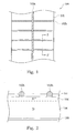
- FIG. 1 illustrates a top view of a solar energy cell according to one preferred embodiment of this invention
- Fig. 2 illustrates a cross-sectional view taken along the line 2-2' of Fig. 1
- a solar energy cell 100 includes a photoelectric conversion layer for converting solar energy into electrical energy.
- the photoelectric conversion layer is formed from a N-type semiconductor layer 104 located on a P-type semiconductor substrate 106, such that a P-N conjunction with electric fields is formed therebetween. Therefore, when the P-N conjunction receives photons, positive charge carriers and negative charge carriers are generated, thereby producing electrical currents.
- This mechanism is also referred as a photoelectric conversion mechanism".
- An anti-reflection layer 101 is formed on a light-receiving side of the N-type semiconductor layer 104 and the P-type semiconductor substrate 106 to reduce the reflective loss of the solar energy cell 100.
- the anti-reflection layer 101 can be silicon nitride or silicon oxide deposited thereon by evaporation, sputtering, screen printing, chemical vapor deposition or other techniques known by those skilled in the art.
- the anti-reflection layer 101 is formed over the photoelectric conversion layer according to a desired color. In particular, a thickness of the anti-reflection layer 101 is determined according to the desired color.
- one or more electrical conductive channels 108 are formed on a bottom side of the N-type semiconductor layer 104 and the P-type semiconductor substrate 106 to output electrical current generated by the photoelectric conversion layer.
- a plurality of electrical conductive channels (102a, 102b) are formed over the anti-reflection layer 101 and electrically connected with the N-type semiconductor layer 104.
- the electrical conductive channels 102b of a smaller cross-section collect and transfer electrical current to the electrical conductive channels 102a of a larger cross-section for external uses.
- the electrical conductive channels (102a, 102b) are made from conductive pastes and pigments to enable their colors to be the same as a color of the anti-reflection layer 101 such that the light-receiving side of the solar energy cell can be of the same color to enhance decorative or visual purposes.
- the electrical conductive channel can include pigments to become a blue electrical conductive channel.
- Fig. 2 only illustrates a cross-sectional design related to the present invention, and other conventional structures, e.g., waterproof designs or front glass, are omitted.
- the conductive paste can include silver powders, glass frits and organic vehicles, but is not limited to those ingredients.
- the pigments can be organic pigments, inorganic pigments, synthetic pigments or any combinations thereof.
- the organic pigments can be monazo, diazo, anthraquinone, indigoid, phthalocyanine or any combinations thereof.
- the inorganic pigments can be titanium dioxide, limonite, malachite, zinc oxide, manganese dioxide or any combinations thereof.
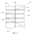
- FIG. 3 illustrates a top view of a solar energy cell 100' according to another preferred embodiment of this invention.
- the solar energy cell 100' is different from the solar energy cell 100 in that the solar energy cell 100' has several different color sections.
- two border lines 110a, 110b are used to divide the anti-reflection layer 101 into three sections (112a, 112b, 112c) of different colors.
- the electrical conductive channels (102a, 102b) within the section 112a of the anti-reflection layer 101 can include proper pigments to enable a color of the electrical conductive channels to be substantially the same as the color of the section 112a.
- the electrical conductive channels (102a, 102b) within the section 112b of the anti-reflection layer 101 can include proper pigments to enable a color of the electrical conductive channels to be substantially the same as the color of the section 112b.
- the electrical conductive channels (102a, 102b) within the section 112c of the anti-reflection layer 101 can include proper pigments to enable a color of the electrical conductive channels to be substantially the same as the color of the section 112c.
- the solar energy cell 100' may include only two different color sections or more than three different color sections according to actual demands so as to achieve desired decorative or visual effects.
- the conductive paste can include silver powders, glass frits and organic vehicles, but is not be limited to those ingredients.
- the pigments can be organic pigments, inorganic pigments, synthetic pigments or any combinations thereof.
- the organic pigments can be monazo, diazo, anthraquinone, indigoid, phthalocyanine or any combinations thereof.
- the inorganic pigments can be titanium dioxide, limonite, malachite, zinc oxide, manganese dioxide or any combinations thereof.
- the solar energy cell disclosed herein has its electrical conductive channel on the light-receiving side to include proper pigments to enable its color to be substantially the same as a color of the entire anti-reflection layer or a color of a surrounding section of the anti-reflection layer according to actual demands, thereby achieving desired decorative or visual effects.
Landscapes
- Photovoltaic Devices (AREA)
- Electrodes Of Semiconductors (AREA)
Applications Claiming Priority (1)
| Application Number | Priority Date | Filing Date | Title |
|---|---|---|---|
| TW100131533A TWI431790B (zh) | 2011-09-01 | 2011-09-01 | 太陽能電池 |
Publications (1)
| Publication Number | Publication Date |
|---|---|
| EP2565932A1 true EP2565932A1 (de) | 2013-03-06 |
Family
ID=45002734
Family Applications (1)
| Application Number | Title | Priority Date | Filing Date |
|---|---|---|---|
| EP20110189432 Ceased EP2565932A1 (de) | 2011-09-01 | 2011-11-16 | Solarenergiezelle |
Country Status (5)
| Country | Link |
|---|---|
| US (1) | US20130056055A1 (de) |
| EP (1) | EP2565932A1 (de) |
| JP (1) | JP2013055310A (de) |
| CN (1) | CN102969385A (de) |
| TW (1) | TWI431790B (de) |
Citations (5)
| Publication number | Priority date | Publication date | Assignee | Title |
|---|---|---|---|---|
| US3904453A (en) * | 1973-08-22 | 1975-09-09 | Communications Satellite Corp | Fabrication of silicon solar cell with anti reflection film |
| EP0751575A2 (de) * | 1995-06-28 | 1997-01-02 | Canon Kabushiki Kaisha | Photovoltaische Zelle und Herstellungsverfahren |
| US20090151771A1 (en) * | 2007-12-17 | 2009-06-18 | Qualcomm Mems Technologies, Inc. | Photovoltaics with interferometric ribbon masks |
| WO2010044901A1 (en) * | 2008-10-16 | 2010-04-22 | Qualcomm Mems Technologies, Inc. | Monolithic imod color enhanced photovoltaic cell |
| US20100279454A1 (en) * | 2009-04-29 | 2010-11-04 | Hans-Juergen Eickelmann | Method of Manufacturing a Solar Cell |
Family Cites Families (15)
| Publication number | Priority date | Publication date | Assignee | Title |
|---|---|---|---|---|
| JPS5333591A (en) * | 1976-09-09 | 1978-03-29 | Japan Solar Energy | Photoelectric converter |
| JP2942895B2 (ja) * | 1989-12-13 | 1999-08-30 | 大日精化工業株式会社 | 導電性床材の製造方法 |
| JP2824882B2 (ja) * | 1992-07-15 | 1998-11-18 | 株式会社 オプトテクノ | 太陽電池装置 |
| JPH08107230A (ja) * | 1994-10-04 | 1996-04-23 | Nissin Electric Co Ltd | 太陽電池パネル |
| JP3050064B2 (ja) * | 1994-11-24 | 2000-06-05 | 株式会社村田製作所 | 導電性ペースト、この導電性ペーストからなるグリッド電極が形成された太陽電池及びその製造方法 |
| JPH10313126A (ja) * | 1997-05-13 | 1998-11-24 | Sharp Corp | 太陽電池素子及びその電極の表面処理方法及び太陽電池モジュール |
| EP0986109A4 (de) * | 1998-03-25 | 2005-01-12 | Tdk Corp | Solarbatterie-Modul |
| JPH11322361A (ja) * | 1998-05-08 | 1999-11-24 | Asahi Glass Co Ltd | 導電性ペースト及び導電体付ガラス板 |
| JP2001345458A (ja) * | 2000-05-30 | 2001-12-14 | Kyocera Corp | 太陽電池 |
| JP4572023B2 (ja) * | 2000-07-11 | 2010-10-27 | 株式会社槌屋 | 着色導電ペーストおよびそれを用いる導電積層体とその製造方法 |
| WO2002021602A1 (en) * | 2000-09-08 | 2002-03-14 | Akzo Nobel N.V. | Colored solar cell unit |
| KR100863408B1 (ko) * | 2007-04-03 | 2008-10-14 | 주식회사 엘지화학 | 흑화처리된 전자파 차폐 유리 및 그 제조방법 |
| TWI493605B (zh) * | 2008-06-11 | 2015-07-21 | Ind Tech Res Inst | 背面電極層的製造方法 |
| JP5703539B2 (ja) * | 2009-01-30 | 2015-04-22 | 旭硝子株式会社 | ガラス組成物 |
| KR101683882B1 (ko) * | 2009-12-24 | 2016-12-21 | 엘지이노텍 주식회사 | 고효율 실리콘 태양전지 전면전극 형성용 페이스트 조성물 및 이를 포함하는 실리콘 태양전지 |
-
2011
- 2011-09-01 TW TW100131533A patent/TWI431790B/zh not_active IP Right Cessation
- 2011-09-13 CN CN2011102764355A patent/CN102969385A/zh active Pending
- 2011-11-01 JP JP2011240105A patent/JP2013055310A/ja active Pending
- 2011-11-10 US US13/293,789 patent/US20130056055A1/en not_active Abandoned
- 2011-11-16 EP EP20110189432 patent/EP2565932A1/de not_active Ceased
Patent Citations (5)
| Publication number | Priority date | Publication date | Assignee | Title |
|---|---|---|---|---|
| US3904453A (en) * | 1973-08-22 | 1975-09-09 | Communications Satellite Corp | Fabrication of silicon solar cell with anti reflection film |
| EP0751575A2 (de) * | 1995-06-28 | 1997-01-02 | Canon Kabushiki Kaisha | Photovoltaische Zelle und Herstellungsverfahren |
| US20090151771A1 (en) * | 2007-12-17 | 2009-06-18 | Qualcomm Mems Technologies, Inc. | Photovoltaics with interferometric ribbon masks |
| WO2010044901A1 (en) * | 2008-10-16 | 2010-04-22 | Qualcomm Mems Technologies, Inc. | Monolithic imod color enhanced photovoltaic cell |
| US20100279454A1 (en) * | 2009-04-29 | 2010-11-04 | Hans-Juergen Eickelmann | Method of Manufacturing a Solar Cell |
Also Published As
| Publication number | Publication date |
|---|---|
| JP2013055310A (ja) | 2013-03-21 |
| TW201312780A (zh) | 2013-03-16 |
| US20130056055A1 (en) | 2013-03-07 |
| CN102969385A (zh) | 2013-03-13 |
| TWI431790B (zh) | 2014-03-21 |
Similar Documents
| Publication | Publication Date | Title |
|---|---|---|
| EP2388827B1 (de) | Solarzellenmodul | |
| US8058549B2 (en) | Photovoltaic devices with integrated color interferometric film stacks | |
| EP2154727B1 (de) | Solarzellen mit Farbanpassung und Verfahren zu ihrer Herstellung | |
| EP2494607B1 (de) | Polarisationsresistente solarzelle | |
| US20080257399A1 (en) | Bifacial thin film solar cell and method for making the same | |
| TWI653764B (zh) | 具有改善能見度的光伏裝置及其製造方法 | |
| WO2008108990A1 (en) | Spectrally adaptive multijunction photovoltaic thin film device and method of producing same | |
| CN103515360A (zh) | 太阳能电池模块和应用于太阳能电池模块的带组件 | |
| CN102064213A (zh) | 外加电场效应薄膜光伏电池及与电场源集成的光伏电池板 | |
| US9153713B2 (en) | Solar cell modules and methods of manufacturing the same | |
| WO2010150833A1 (ja) | 薄膜複合電池およびその製造方法 | |
| JP6034791B2 (ja) | 太陽光発電装置 | |
| EP2600422A2 (de) | Vorrichtung zur solarstromgewinnung und herstellungsverfahren dafür | |
| EP3139418B1 (de) | Solarzellenmodul | |
| EP3518294B1 (de) | Solarzellenmodul mit einem verdrahtungsleitungsmaterial zur verbindung von solarzellen | |
| JP2006210780A (ja) | 多層型光電変換装置 | |
| US20130056055A1 (en) | Solar energy cell | |
| KR101250207B1 (ko) | 다색 그림 태양전지 제조방법 | |
| CN110650606A (zh) | 壳体及其制备方法和电子设备 | |
| JP2018037481A (ja) | 太陽電池モジュールおよび太陽電池モジュールの製造方法 | |
| CN110650227A (zh) | 壳体机构及电子设备 | |
| CN110504364A (zh) | 钙钛矿电池及具有其的标示牌 | |
| EP2579333A2 (de) | Solarzelle und verfahren zu ihrer herstellung | |
| EP4250376A1 (de) | Solarzellen und herstellungsverfahren davon | |
| CN217086598U (zh) | 新型光电池器件 |
Legal Events
| Date | Code | Title | Description |
|---|---|---|---|
| PUAI | Public reference made under article 153(3) epc to a published international application that has entered the european phase |
Free format text: ORIGINAL CODE: 0009012 |
|
| 17P | Request for examination filed |
Effective date: 20111116 |
|
| AK | Designated contracting states |
Kind code of ref document: A1 Designated state(s): AL AT BE BG CH CY CZ DE DK EE ES FI FR GB GR HR HU IE IS IT LI LT LU LV MC MK MT NL NO PL PT RO RS SE SI SK SM TR |
|
| AX | Request for extension of the european patent |
Extension state: BA ME |
|
| 17Q | First examination report despatched |
Effective date: 20140714 |
|
| STAA | Information on the status of an ep patent application or granted ep patent |
Free format text: STATUS: THE APPLICATION HAS BEEN REFUSED |
|
| 18R | Application refused |
Effective date: 20151122 |