EP2568496A2 - Verfahren und Vorrichtung zur Aufrechterhaltung der Betriebstemperatur einer integrierten Schaltung - Google Patents
Verfahren und Vorrichtung zur Aufrechterhaltung der Betriebstemperatur einer integrierten Schaltung Download PDFInfo
- Publication number
- EP2568496A2 EP2568496A2 EP12183704A EP12183704A EP2568496A2 EP 2568496 A2 EP2568496 A2 EP 2568496A2 EP 12183704 A EP12183704 A EP 12183704A EP 12183704 A EP12183704 A EP 12183704A EP 2568496 A2 EP2568496 A2 EP 2568496A2
- Authority
- EP
- European Patent Office
- Prior art keywords
- heat
- secure
- transfer element
- secure element
- transfer
- Prior art date
- Legal status (The legal status is an assumption and is not a legal conclusion. Google has not performed a legal analysis and makes no representation as to the accuracy of the status listed.)
- Withdrawn
Links
Images


Classifications
-
- H—ELECTRICITY
- H10—SEMICONDUCTOR DEVICES; ELECTRIC SOLID-STATE DEVICES NOT OTHERWISE PROVIDED FOR
- H10W—GENERIC PACKAGES, INTERCONNECTIONS, CONNECTORS OR OTHER CONSTRUCTIONAL DETAILS OF DEVICES COVERED BY CLASS H10
- H10W40/00—Arrangements for thermal protection or thermal control
- H10W40/10—Arrangements for heating
Definitions
- the present disclosure is generally directed toward a temperature-controlled integrated circuit and specifically directed toward a temperature-controlled integrated circuit comprising a secure data processing element which operates in an extended temperature range.
- Secure access systems are used in a wide array of settings spanning industrial, medical, military, retail and financial. In addition to controlling access, the systems may also monitor and record access, track user behavior and detect access irregularities such as fraudulent access cards.
- Typical secure access systems employ a fixed control reader device and a user access card, commonly communicating through a magnetic stripe embedded on the access card or via radio frequency (RF).
- RFID radio frequency
- an access card located within a given proximity to a card reader communicates through electromagnetic waves in the RF band.
- Secure cards include a secure data processing component to authenticate a valid user. Secure access systems employing RFID is generally discussed in US Patent Application Publication No. 2007/0001008 , the entire contents of which are hereby incorporated by reference.
- Access control readers used in secure access systems are typically limited in operating environments to a nominal temperature band, commonly above 0 degree Celsius. Such an operating limitation can significantly decrease the utility of secure access systems, in particular those mounted outdoors in cold-weather climates. Any expansion of the operating envelope of such systems must be cost-efficient, simple to implement, reliable, and secure, given the highly cost-competitive nature of secure access systems and access readers / access card systems.
- US Patent No. 6,042,010 One example of a system intended to expand the operating temperature range of card readers is disclosed in US Patent No. 6,042,010 , the entire contents of which are hereby incorporated by reference.
- the '010 patent employs specialized structure on a card reader to prevent foreign material from invading the circuit unit.
- a magnetic head holding means protrudes from the card reader main unit to the inside of the card insertion slot cover.
- US Patent No. 7,438,220 discloses a system to control the temperature of a secure system.
- the entire contents of the '220 patent are hereby incorporated by reference.
- the '220 publication describes an automated banking machine with a card reader involving a complex temperature control system for the reader.
- the '220 device is impractical for adaptation to most access control systems and is not particularly cost-effective.
- thermocontroller it is, therefore, one aspect of the present disclosure to provide a temperature-controlled integrated circuit comprising a heat-transfer element which allows a secure data processing element to operate in an extended operating range. It is also an aspect of the present disclosure to provide easy-to-implement and cost-effective methods of constructing and using a temperature-controlled integrated circuit comprising a heat-transfer element.
- the temperature-controlled integrated circuit is fitted with a heat-transfer element positioned on a common substrate with the secure element.
- the heat-transfer element is configured to transfer thermal energy, such as heat, to the secure element, thereby allowing the secure element to operate at a lower temperature than its nominal operating temperature range would predict.
- the heat-transfer element such as a surface mount resistor, is configured to generate heat as prompted by any of several events. For example, heat may be generated after an atmospheric temperature is sensed below the nominal lowest operating temperature, as measured on the device itself or adjacent the device, or due to a state of communication between the secure element and a general purpose processor (such as a lack of communication or a degradation in communication).
- Fig. 1A is a top-view of a temperature-controlled integrated circuit in accordance with at least some embodiments of the present disclosure
- Fig. 1B is a cross-sectional side-view of a temperature-controlled integrated circuit in accordance with at least some embodiments of the present disclosure
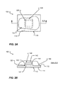
- Fig. 2A is a top-view of a temperature-controlled integrated circuit in accordance with some embodiments of the present disclosure
- Fig. 2B is a cross-sectional side-view of a temperature-controlled integrated circuit in accordance with some embodiments of the present disclosure
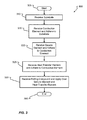
- Fig. 3 is a flow-diagram representation of a method of manufacture of a temperature-controlled integrated circuit in accordance with at least some embodiments of the present disclosure
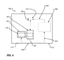
- Fig. 4 is a top-view of a temperature-controlled integrated circuit in an access control reader environment.
- Fig. 5 is a flow diagram of an embodiment of a method of use of a temperature-controlled integrated circuit in accordance with at least some embodiments of the present disclosure.
- FIGs. 1-5 representations and configurations of the device, methods of manufacture of the device, and methods of use of the device are shown.
- FIGs. 1-5 representations and configurations of the device, methods of manufacture of the device, and methods of use of the device are shown.
- Figs. 1A-B corresponding top and cross-sectional side views of the device 100 are provided.
- Fig. 1A is a top-view of the temperature-controlled integrated circuit device 100 and
- Fig. 1B is the corresponding cross-sectional side view along section line A-A.
- a temperature-controlled integrated circuit device 100 and components thereof will be described in accordance with at least some embodiments of the present disclosure.
- the term temperature-controlled integrated circuit device, integrated-circuit (“IC") device, IC device or device as used herein includes a completed temperature-controlled integrated circuit device or any intermediate temperature-controlled integrated circuit device (e.g., those not including power hook-ups).
- IC integrated-circuit
- Figs. 1A-B depict a first example of a temperature-controlled integrated circuit device 100 having a substrate 110, a secure element 130, a heat-transfer element 140, a conductive element 120, and potting compound 150.
- the substrate 110 has a lower surface 111 and upper surface 112.
- the conductive element 120 has a lower surface 121 and upper surface 122.
- the secure element 130 has a lower surface 131 and upper surface 132
- the heat-transfer element 140 has a lower surface 141 and upper surface 142.
- the conductive element 120 is disposed on the substrate 110, such that the upper surface 112 of the substrate 110 engages the lower surface 121 of the conductive element 120.
- the secure element 130 and the heat-transfer element 140 are disposed side-by-side on the conductive element 120.
- the lower surface 131 of the secure element 130 engages the upper surface 122 of the conductive element 120
- the lower surface 141 of the heat-transfer element 140 engages the upper surface 122 of the conductive element 120.
- Potting compound 150 is at least partially disposed over the stack of substrate 110, secure element 130, heat-transfer element 140 and conductive element 120, such that potting compound 150 engages one or more of the upper surface 112 of the substrate 110, the upper surface 122 of the conductive element 120, the upper surface 132 of the secure element 130, and the upper surface 142 of the heat-transfer element 140.
- the device 100 depicted in Figs. 1A-B is devoid of a conductive element 120, and each of secure element 130 and heat-transfer element 140 are thus disposed on the substrate 110. It may also be possible to dispose the conductive element 120 on top of the secure element 130 and heat-transfer element 140 if such devices are mounted on the upper surface of the substrate 112. In such an arrangement, the lower surface of the conductive element 121 may be in direct contact with the upper surface of the secure element 132 and the upper surface of the heat-transfer element 142.
- FIG. 2A-B An alternative arrangement for the device 100 is depicted in Figs. 2A-B.
- Figs. 2A-B provide corresponding top and cross-sectional side views of the device 100.
- Fig. 2A is a top-view of the temperature-controlled integrated circuit device 100 and
- Fig. 2B is the corresponding cross-sectional side view along section line A-A.
- Figs. 2A-B depict a temperature-controlled integrated circuit device 100 having a substrate 110, a secure element 130, a heat-transfer element 140, and potting compound 150.
- the substrate 110 has a lower surface 111 and upper surface 112.
- the secure element 130 has a lower surface 131 and upper surface 132, and the heat-transfer element 140 has a lower surface 141 and upper surface 142.
- the secure element 130 disposed on the substrate 110 such that the upper surface 112 of the substrate 110 engages the lower surface 131 of the secure element 130.
- the heat-transfer element 140 is disposed on top of the secure element 130, such that the lower surface 141 of the heat-transfer element 140 engages the upper surface 132 of the secure element 130.
- Potting compound 120 is disposed at least partially over the stack of substrate 110, secure element 130, and heat-transfer element 140, such that potting compound 150 engages one or more of the upper surface 112 of the substrate 110, the upper surface 132 of the secure element 130, and the upper surface 142 of the heat-transfer element 140.
- the device 100 depicted in Figs. 2A-B has a conductive element 120 positioned between the secure element 130 and the substrate 110.
- the substrate 110 of the device 100 can be constructed of a flexible, rigid or semi-rigid material.
- the aforementioned elements of the device 100 are constructed of a plastic material or plastic composite.
- the material may comprise polyethylene terephthalate (PET), polyethylene terephthalate glycol (PET G), crystalline PET (PET-C) i.e. a biaxially stretched polyethylene terephthalate.
- PET polyethylene terephthalate
- PET G polyethylene terephthalate glycol
- PET-C crystalline PET
- the substrate may be a printed circuit board (PCB) and/or any material known to one skilled in the art for use as a PCB or a backing plane for an integrated circuit.
- PCB printed circuit board
- the secure element 130 may be configured to perform secure data processing.
- the secure element 130 may be a secure access module (SAM) and/or a secure embedded element (SEM) and/or a subscriber identity module (SIM).
- SAM secure access module
- SEM secure embedded element
- SIM subscriber identity module
- a secure element refers to any certified tamper-resistant platform, capable of securely hosting applications and their confidential and cryptographic data in accordance with rules and security requirements set forth by a trusted authority.
- Examples of secure elements include Universal Integrated Circuit Cards (UICCs), embedded secure elements, and removable secure elements. More specific examples of removable secure elements include SAMs, micro Secure Digital (SD) cards, miniSD cards, SIM cards, and the like.
- the heat-transfer element 140 may, in some embodiments, be a resistor or collection of resistors.
- the surface mount resistor is preferably between 2 and 100 ohms, more preferably between 5 and 80 ohms, and most preferably between 10 and 50 ohms.
- the heat-transfer element 140 may be an axial leaded resistor or any surface mount device (SMD) capable of generating heat.
- SMD surface mount device
- the device 100 may be configured to operate in an environment of an access control reader.
- the conductive element 120 may be made of a material consisting of copper, aluminum, titanium, tungsten, silicon carbide, a conductive epoxy, a conductive polymer, a metal and any material known to one skilled in the art to act as a conductive element.
- the conductive element 120 is a plate. Additional disclosure regarding conductive plates may be found in US Patent Nos. 5,089,876 ; 5,396,403 ; and 6,330,145 , each of which are incorporated by reference in their entireties.
- Potting compound 150 may be disposed substantially over one or more of the secure element 130 and heat-transfer element 140, where the phrase "substantially over” is understood to mean to cover no less than 50 percent of the compared surface area, e.g. to cover no less than 50 percent of the surface area of the upper surface 142 of the heat-transfer element 140.
- the potting compound 150 may be any compound known to one skilled in the art as used in integrated circuits. Most preferable the compound is any compound that acts as a thermally-conductive compound.
- any one or more of the secure element 130, heat-transfer element 140, and conductive element 120 may be disposed and/or adhered to one another and/or the substrate 110 by any of several methods know to those skilled in the art, to include standard methods of soldering surface mounted components (SMCs) to PCBs.
- SMCs surface mounted components
- U.S. 2004/007324 and WO 2009/1063058 disclose common adhesion methods, both of which are hereby incorporated herein by reference in their entireties. It should be appreciated that the above-mentioned documents are non-limiting examples of the types of methods that may be employed. Other known or yet-to-be-developed mechanisms are also considered to be within the scope of the present disclosure.
- the device 100 depicted in Figs. 1A-B or Figs. 2A-B is devoid of potting compound 150.
- the potting compound 150 is shown as a continuous, single structure, in other embodiments the potting compound is a plurality of structures and/or not a continuous structure.
- embodiments of the present disclosure generally describe the manufacturing process to involve attaching, disposing and/or positioning the secure element 130, heat-transfer element 140, conductive element 120 and potting compound 150 to the substrate 110, it should be appreciated that embodiments of the present disclosure also contemplate attaching, disposing and/or positioning the secure element 130 and heat-transfer element 140 to the substrate 110 without one or both of attaching, disposing and/or positioning the conductive element 120 and potting compound 150 to the substrate 110.
- the nominal operating range of the secure element 130 is between about -35 degree Celsius and +65 degree Celsius. In another embodiment, the nominal operating range of the secure element 130 is above 0 degree Celsius.
- FIG. 3 is a flow diagram of the process.
- FIG. 3 A general order for the steps of the method 300 of a method of manufacture is shown in Fig. 3 .
- the method 300 starts with a start operation 305 and ends with an end operation 395.
- the method 300 can include more or fewer steps or can arrange the order of the steps differently than those shown in Fig. 3 .
- the method 300 produces an embodiment of the temperature-controlled integrated circuit device 100 of the type shown in Figs. 1A-B .
- a sheet of substrate 110 is received, as depicted in step 310.
- the sheet 110 would typically be sized to allow a plurality of IC devices 100 to be manufactured, although the sheet 110 could also be configured to produce one device 100 at a time.
- step 315 the conductive element 120 is received and adhered to the substrate 110.
- Any of several methods know to those skilled in the art for adhering electrical and/or IC components to a substrate may be used, to include various glues and welding technologies.
- step 320 the secure element 130 is received and positioned on the conductive element 120.
- the secure element 130 is positioned on the conductive element 120 such that sufficient space is provided on the conductive element 120 to allow the subsequent positioning of the heat-transfer element on the conductive element 120.
- the secure element 130 is adhered to the conductive element 120.
- step 325 the heat-transfer element 140 is received and positioned on the conductive element 120.
- the heat-transfer element 140 is positioned on the conductive element 120 relative to the position of the secure element 130 so as to allow the heat-transfer element 140 to transfer heat to the secure element 130.
- the heat-transfer element 140 is adhered to the conductive element 120.
- step 330 potting compound 330 is received and applied over at least a portion of the upper surface 132 of the secure element 130 and the upper surface 142 of the heat-transfer element 140, and at least a portion of the upper surface 112 of the substrate 110.
- the potting compound may be applied so as to create a single, continuous structure as depicted in Figs. 1A-B or, alternatively, as a set of multiple structures.
- the process ends at step 395 in producing one or more temperature-controlled integrated circuit devices 100.
- Fig. 4 is a top-view of a temperature-controlled integrated circuit device 100 in an access control reader environment.
- the device 100 is depicted in the embodiment of Figs. 1A-B , except that the potting compound 150 has been removed for clarity. Additional components of an access control reader are not shown in Fig. 4 .
- Fig. 4 depicts a temperature-controlled integrated circuit device 100 having a substrate 410, a secure element 130, a heat-transfer element 140 and a conductive element 120.
- the substrate 110 has an upper surface 412.
- the conductive element 120 is disposed on the substrate 410, such that the upper surface 412 of the substrate 110 engages the lower surface of the conductive element 120.
- the secure element 130 and the heat-transfer element 140 are disposed side-by-side on the conductive element 120.
- the lower surface of the secure element 130 engages the upper surface of the conductive element 120, and the lower surface of the heat-transfer element 140 engages the upper surface of the conductive element 120.
- Potting compound is disposed at least partially over one or more of the stack of secure element 130, heat-transfer element 140 and conductive element 120 as well as another other components on the substrate 410 (e.g., general purpose microprocessor 400).
- a general purpose microprocessor 400 is in communication 425 with the secure element 130 and is in communication 420, via switch 430 to voltage source 432, with heat-transfer element 140. Heat-transfer element 140 also engages ground 440.
- the general purpose microprocessor 400 controls operations of the secure element 130, such as secure data processing.
- Communications 425 may include input/output, clock, reset, power, and ground.
- communications 425 with the general purpose microprocessor 400 would stop or be interrupted; such a state would be recognized by the general purpose microprocessor 400 and trigger the microprocessor 400 to activate the heat-transfer element 140 by connecting it to voltage source 432 via actuation of the switch 430.
- the general purpose microprocessor 400 may engage the power source 432 through switch 430 so as to provide power to heat-transfer element 140.
- a complete circuit running between general purpose microprocessor 400 to voltage source 432 to surface mount resistor heat-generating element 140 would generate heat.
- the switch 430 is a transistor.
- the general purpose processor 400 acts as the heat-generating element 140.
- the voltage source 432 is between 1-30 volts, in a preferred embodiment the voltage source 432 is between 2-25 volts, and in a most preferred embodiment, the voltage source 432 is between 5-16 volts.
- FIG. 5 is a flow diagram of the process.
- FIG. 5 A general order for the steps of the method 500 of a method of use is shown in Fig. 5 .
- the method 500 starts with a start operation 505 and ends with an end operation 595.
- the method 500 can include more or fewer steps or can arrange the order of the steps differently than those shown in Fig. 5 .
- the method 500 produces an embodiment of the temperature-controlled integrated circuit device 100 that operates in an extended temperature range.
- the temperature-controlled integrated circuit device 100 is exposed to an extended temperature range. That is, the device 100, which is configured to operate within a nominal operating temperature range, is exposed to a temperature below the lowest temperature of that nominal temperature range. For example, a device 100 with a lowest nominal operating temperature of 0 degree Celsius is exposed to a temperature of -10 degree Celsius.
- the device 100 determines that heating is required (so as to allow the device 100 to operate).
- the device 100 may determine heating is required in any of several ways, to include receiving an input from a sensor that senses at least one of an atmospheric temperature adjacent the system is below the nominal lowest operating temperature, a temperature is measured on the device itself that similarly indicates that the system is below the nominal lowest operating temperature, and/or a state of the communication between the secure element 130 and a general purpose processor 500 (as depicted in Fig. 4 ).
- a state of the communication between the secure element 130 and the general purpose processor 500 that could trigger the device 100 to apply heat is a no-op state, i.e.
- step 520 the heat-generating element is activated.
- the general purpose microprocessor 400 may engage a power source 432 through switch 430 so as to provide power to heat-generating element 140.
- step 525 heat is applied to the device 100.
- a complete circuit running between general purpose microprocessor 400 to voltage source 432 to surface mount resistor heat-generating element 140 would generate heat given current running through the resistor.
- the present disclosure in various aspects, embodiments, and/or configurations, includes components, methods, processes, systems and/or apparatus substantially as depicted and described herein, including various aspects, embodiments, configurations embodiments, subcombinations, and/or subsets thereof.
- the present disclosure in various aspects, embodiments, and/or configurations, includes providing devices and processes in the absence of items not depicted and/or described herein or in various aspects, embodiments, and/or configurations hereof, including in the absence of such items as may have been used in previous devices or processes, e.g., for improving performance, achieving ease and ⁇ or reducing cost of implementation.
Landscapes
- Cooling Or The Like Of Semiconductors Or Solid State Devices (AREA)
- Logic Circuits (AREA)
- Semiconductor Integrated Circuits (AREA)
Applications Claiming Priority (1)
| Application Number | Priority Date | Filing Date | Title |
|---|---|---|---|
| US201161532961P | 2011-09-09 | 2011-09-09 |
Publications (2)
| Publication Number | Publication Date |
|---|---|
| EP2568496A2 true EP2568496A2 (de) | 2013-03-13 |
| EP2568496A3 EP2568496A3 (de) | 2017-12-06 |
Family
ID=46940296
Family Applications (1)
| Application Number | Title | Priority Date | Filing Date |
|---|---|---|---|
| EP12183704.1A Withdrawn EP2568496A3 (de) | 2011-09-09 | 2012-09-10 | Verfahren und Vorrichtung zur Aufrechterhaltung der Betriebstemperatur einer integrierten Schaltung |
Country Status (2)
| Country | Link |
|---|---|
| US (1) | US9917028B2 (de) |
| EP (1) | EP2568496A3 (de) |
Cited By (1)
| Publication number | Priority date | Publication date | Assignee | Title |
|---|---|---|---|---|
| US11657913B2 (en) | 2019-08-23 | 2023-05-23 | Koninklijke Philips N.V. | Generating a clinician-perceptible output responsive to a subject-monitoring device |
Citations (8)
| Publication number | Priority date | Publication date | Assignee | Title |
|---|---|---|---|---|
| US5089876A (en) | 1989-07-19 | 1992-02-18 | Nec Corporation | Semiconductor ic device containing a conductive plate |
| US5396403A (en) | 1993-07-06 | 1995-03-07 | Hewlett-Packard Company | Heat sink assembly with thermally-conductive plate for a plurality of integrated circuits on a substrate |
| US6042010A (en) | 1997-01-10 | 2000-03-28 | Matsushita Electric Industrial Co., Ltd. | Card reader and a method of installing a card reader |
| US6330145B1 (en) | 1998-12-30 | 2001-12-11 | Stmicroelectronics, Inc. | Apparatus and method for contacting a sensor conductive layer |
| US20040007324A1 (en) | 2000-05-20 | 2004-01-15 | Ralf Henn | Method for producing document cards comprising several layers and document cards produced therewith |
| US20070001008A1 (en) | 2003-12-05 | 2007-01-04 | Hid Corporation | Low voltage signal stripping circuit for an RFID reader |
| US7438220B2 (en) | 2002-11-25 | 2008-10-21 | Diebold Self-Service Systems Division Of Diebold, Incorporated | Automated banking machine including deposit storage chest and card reader cooling device |
| WO2009106305A2 (en) | 2008-02-27 | 2009-09-03 | Carl Zeiss Smt Ag | Method of bonding two components by,,fusion bonding" to form a bonded structure |
Family Cites Families (12)
| Publication number | Priority date | Publication date | Assignee | Title |
|---|---|---|---|---|
| US5640746A (en) * | 1995-08-15 | 1997-06-24 | Motorola, Inc. | Method of hermetically encapsulating a crystal oscillator using a thermoplastic shell |
| FR2739706B1 (fr) | 1995-10-09 | 1997-11-21 | Inside Technologies | Perfectionnements aux cartes a memoire |
| FR2748333B1 (fr) | 1996-05-06 | 1998-11-27 | Inside Technologies | Procede pour selectionner un module electronique parmi une pluralite de modules presents dans le champ d'interrogation d'un terminal |
| US5917272A (en) * | 1998-06-11 | 1999-06-29 | Vectron, Inc. | Oven-heated crystal resonator and oscillator assembly |
| EP1058216B1 (de) | 1999-06-04 | 2002-12-11 | D'Udekem D'Acoz, Xavier Guy Bernard | Speicherkarte |
| US6494367B1 (en) | 1999-10-15 | 2002-12-17 | Ajit Kumar Zacharias | Secure multi-application card system |
| US6650227B1 (en) | 1999-12-08 | 2003-11-18 | Hid Corporation | Reader for a radio frequency identification system having automatic tuning capability |
| JP4354347B2 (ja) * | 2004-06-29 | 2009-10-28 | 日本電波工業株式会社 | 水晶発振器 |
| US7124943B2 (en) | 2004-09-24 | 2006-10-24 | Assa Abloy Identification Technology Group Ab | RFID system having a field reprogrammable RFID reader |
| JP4804813B2 (ja) * | 2005-06-24 | 2011-11-02 | 日本電波工業株式会社 | 圧電発振器 |
| US7782147B2 (en) * | 2007-06-20 | 2010-08-24 | Motorola, Inc. | Apparatus for providing oscillator frequency stability |
| CN201867439U (zh) | 2010-08-04 | 2011-06-15 | 中国电力科学研究院 | 一种低温工作补偿装置 |
-
2012
- 2012-09-10 EP EP12183704.1A patent/EP2568496A3/de not_active Withdrawn
- 2012-09-10 US US13/607,981 patent/US9917028B2/en active Active
Patent Citations (8)
| Publication number | Priority date | Publication date | Assignee | Title |
|---|---|---|---|---|
| US5089876A (en) | 1989-07-19 | 1992-02-18 | Nec Corporation | Semiconductor ic device containing a conductive plate |
| US5396403A (en) | 1993-07-06 | 1995-03-07 | Hewlett-Packard Company | Heat sink assembly with thermally-conductive plate for a plurality of integrated circuits on a substrate |
| US6042010A (en) | 1997-01-10 | 2000-03-28 | Matsushita Electric Industrial Co., Ltd. | Card reader and a method of installing a card reader |
| US6330145B1 (en) | 1998-12-30 | 2001-12-11 | Stmicroelectronics, Inc. | Apparatus and method for contacting a sensor conductive layer |
| US20040007324A1 (en) | 2000-05-20 | 2004-01-15 | Ralf Henn | Method for producing document cards comprising several layers and document cards produced therewith |
| US7438220B2 (en) | 2002-11-25 | 2008-10-21 | Diebold Self-Service Systems Division Of Diebold, Incorporated | Automated banking machine including deposit storage chest and card reader cooling device |
| US20070001008A1 (en) | 2003-12-05 | 2007-01-04 | Hid Corporation | Low voltage signal stripping circuit for an RFID reader |
| WO2009106305A2 (en) | 2008-02-27 | 2009-09-03 | Carl Zeiss Smt Ag | Method of bonding two components by,,fusion bonding" to form a bonded structure |
Cited By (1)
| Publication number | Priority date | Publication date | Assignee | Title |
|---|---|---|---|---|
| US11657913B2 (en) | 2019-08-23 | 2023-05-23 | Koninklijke Philips N.V. | Generating a clinician-perceptible output responsive to a subject-monitoring device |
Also Published As
| Publication number | Publication date |
|---|---|
| EP2568496A3 (de) | 2017-12-06 |
| US20130062331A1 (en) | 2013-03-14 |
| US9917028B2 (en) | 2018-03-13 |
Similar Documents
| Publication | Publication Date | Title |
|---|---|---|
| EP3433797B1 (de) | Verfahren zur herstellung einer chipkarte | |
| US9390364B2 (en) | Transponder chip module with coupling frame on a common substrate for secure and non-secure smartcards and tags | |
| US8047445B2 (en) | Wireless IC device and method of manufacturing the same | |
| EP2973238B1 (de) | Informationstragende karte zur anzeige einmaliger passcodes und verfahren zur herstellung davon | |
| CN103119616A (zh) | 聚碳酸酯制射频识别设备及其制造方法 | |
| US11386317B2 (en) | Transponder chip module with module antenna(s) and coupling frame(s) | |
| JP2010504583A (ja) | 電子カードとその製造方法 | |
| WO2010019851A2 (en) | Rfid card with piezoelectric element | |
| CN108885708A (zh) | 制造智能卡的方法 | |
| WO2015144261A1 (en) | Transponder chip module with coupling frame on a common substrate for secure and non-secure smartcards and tags | |
| JP6114677B2 (ja) | プリントされた無線周波数識別(rfid)タグに関する装置および方法 | |
| CN110832506A (zh) | 干扰优化的金属制数据载体 | |
| CN105512715A (zh) | 芯片卡模块装置、芯片卡装置和用于制造芯片卡装置的方法 | |
| EP3948667B1 (de) | Verbesserte karte mit fingerabdruckbiometriken | |
| US9917028B2 (en) | Method and apparatus for maintaining operational temperature of an integrated circuit | |
| CN114757319A (zh) | 用于制造抗龟裂电子设备的方法 | |
| JP2015075782A (ja) | アンテナシートと非接触icカード | |
| JP4675184B2 (ja) | Icタグ | |
| JP2007257620A (ja) | 非接触icタグ | |
| WO2007069802A1 (en) | Radio frequency identification tag for the metal product with high thermal resistance and the fabricating method thereof | |
| WO2022243432A1 (en) | Manufacturing a smartcard | |
| JP4848214B2 (ja) | 非接触icタグ | |
| KR102856550B1 (ko) | 전자 카드 제조 방법 | |
| KR20080084767A (ko) | 전자카드 모듈 및 그 제조방법 | |
| KR101427339B1 (ko) | 알에프아이디 카드 및 그 제조방법 |
Legal Events
| Date | Code | Title | Description |
|---|---|---|---|
| PUAI | Public reference made under article 153(3) epc to a published international application that has entered the european phase |
Free format text: ORIGINAL CODE: 0009012 |
|
| AK | Designated contracting states |
Kind code of ref document: A2 Designated state(s): AL AT BE BG CH CY CZ DE DK EE ES FI FR GB GR HR HU IE IS IT LI LT LU LV MC MK MT NL NO PL PT RO RS SE SI SK SM TR |
|
| AX | Request for extension of the european patent |
Extension state: BA ME |
|
| PUAL | Search report despatched |
Free format text: ORIGINAL CODE: 0009013 |
|
| AK | Designated contracting states |
Kind code of ref document: A3 Designated state(s): AL AT BE BG CH CY CZ DE DK EE ES FI FR GB GR HR HU IE IS IT LI LT LU LV MC MK MT NL NO PL PT RO RS SE SI SK SM TR |
|
| AX | Request for extension of the european patent |
Extension state: BA ME |
|
| RIC1 | Information provided on ipc code assigned before grant |
Ipc: H01L 23/34 20060101AFI20171030BHEP |
|
| STAA | Information on the status of an ep patent application or granted ep patent |
Free format text: STATUS: THE APPLICATION IS DEEMED TO BE WITHDRAWN |
|
| 18D | Application deemed to be withdrawn |
Effective date: 20180607 |