EP2571065A1 - Dispositif à semi-conducteur à nitrure du groupe iii et procédé de fabrication associé - Google Patents
Dispositif à semi-conducteur à nitrure du groupe iii et procédé de fabrication associé Download PDFInfo
- Publication number
- EP2571065A1 EP2571065A1 EP20110847760 EP11847760A EP2571065A1 EP 2571065 A1 EP2571065 A1 EP 2571065A1 EP 20110847760 EP20110847760 EP 20110847760 EP 11847760 A EP11847760 A EP 11847760A EP 2571065 A1 EP2571065 A1 EP 2571065A1
- Authority
- EP
- European Patent Office
- Prior art keywords
- layer
- group iii
- iii nitride
- nitride semiconductor
- mask layer
- Prior art date
- Legal status (The legal status is an assumption and is not a legal conclusion. Google has not performed a legal analysis and makes no representation as to the accuracy of the status listed.)
- Withdrawn
Links
Images


Classifications
-
- H—ELECTRICITY
- H10—SEMICONDUCTOR DEVICES; ELECTRIC SOLID-STATE DEVICES NOT OTHERWISE PROVIDED FOR
- H10D—INORGANIC ELECTRIC SEMICONDUCTOR DEVICES
- H10D62/00—Semiconductor bodies, or regions thereof, of devices having potential barriers
- H10D62/80—Semiconductor bodies, or regions thereof, of devices having potential barriers characterised by the materials
- H10D62/83—Semiconductor bodies, or regions thereof, of devices having potential barriers characterised by the materials being Group IV materials, e.g. B-doped Si or undoped Ge
- H10D62/832—Semiconductor bodies, or regions thereof, of devices having potential barriers characterised by the materials being Group IV materials, e.g. B-doped Si or undoped Ge being Group IV materials comprising two or more elements, e.g. SiGe
- H10D62/8325—Silicon carbide
-
- H—ELECTRICITY
- H10—SEMICONDUCTOR DEVICES; ELECTRIC SOLID-STATE DEVICES NOT OTHERWISE PROVIDED FOR
- H10H—INORGANIC LIGHT-EMITTING SEMICONDUCTOR DEVICES HAVING POTENTIAL BARRIERS
- H10H20/00—Individual inorganic light-emitting semiconductor devices having potential barriers, e.g. light-emitting diodes [LED]
- H10H20/01—Manufacture or treatment
- H10H20/011—Manufacture or treatment of bodies, e.g. forming semiconductor layers
- H10H20/013—Manufacture or treatment of bodies, e.g. forming semiconductor layers having light-emitting regions comprising only Group III-V materials
- H10H20/0133—Manufacture or treatment of bodies, e.g. forming semiconductor layers having light-emitting regions comprising only Group III-V materials with a substrate not being Group III-V materials
- H10H20/01335—Manufacture or treatment of bodies, e.g. forming semiconductor layers having light-emitting regions comprising only Group III-V materials with a substrate not being Group III-V materials the light-emitting regions comprising nitride materials
-
- H—ELECTRICITY
- H10—SEMICONDUCTOR DEVICES; ELECTRIC SOLID-STATE DEVICES NOT OTHERWISE PROVIDED FOR
- H10H—INORGANIC LIGHT-EMITTING SEMICONDUCTOR DEVICES HAVING POTENTIAL BARRIERS
- H10H20/00—Individual inorganic light-emitting semiconductor devices having potential barriers, e.g. light-emitting diodes [LED]
- H10H20/80—Constructional details
- H10H20/81—Bodies
- H10H20/819—Bodies characterised by their shape, e.g. curved or truncated substrates
-
- H—ELECTRICITY
- H10—SEMICONDUCTOR DEVICES; ELECTRIC SOLID-STATE DEVICES NOT OTHERWISE PROVIDED FOR
- H10P—GENERIC PROCESSES OR APPARATUS FOR THE MANUFACTURE OR TREATMENT OF DEVICES COVERED BY CLASS H10
- H10P14/00—Formation of materials, e.g. in the shape of layers or pillars
- H10P14/20—Formation of materials, e.g. in the shape of layers or pillars of semiconductor materials
- H10P14/22—Formation of materials, e.g. in the shape of layers or pillars of semiconductor materials using physical deposition, e.g. vacuum deposition or sputtering
-
- H—ELECTRICITY
- H10—SEMICONDUCTOR DEVICES; ELECTRIC SOLID-STATE DEVICES NOT OTHERWISE PROVIDED FOR
- H10P—GENERIC PROCESSES OR APPARATUS FOR THE MANUFACTURE OR TREATMENT OF DEVICES COVERED BY CLASS H10
- H10P14/00—Formation of materials, e.g. in the shape of layers or pillars
- H10P14/20—Formation of materials, e.g. in the shape of layers or pillars of semiconductor materials
- H10P14/27—Formation of materials, e.g. in the shape of layers or pillars of semiconductor materials using selective deposition, e.g. simultaneous growth of monocrystalline and non-monocrystalline semiconductor materials
- H10P14/271—Formation of materials, e.g. in the shape of layers or pillars of semiconductor materials using selective deposition, e.g. simultaneous growth of monocrystalline and non-monocrystalline semiconductor materials characterised by the preparation of substrate for selective deposition
-
- H—ELECTRICITY
- H10—SEMICONDUCTOR DEVICES; ELECTRIC SOLID-STATE DEVICES NOT OTHERWISE PROVIDED FOR
- H10P—GENERIC PROCESSES OR APPARATUS FOR THE MANUFACTURE OR TREATMENT OF DEVICES COVERED BY CLASS H10
- H10P14/00—Formation of materials, e.g. in the shape of layers or pillars
- H10P14/20—Formation of materials, e.g. in the shape of layers or pillars of semiconductor materials
- H10P14/29—Formation of materials, e.g. in the shape of layers or pillars of semiconductor materials characterised by the substrates
- H10P14/2901—Materials
- H10P14/2902—Materials being Group IVA materials
- H10P14/2904—Silicon carbide
-
- H—ELECTRICITY
- H10—SEMICONDUCTOR DEVICES; ELECTRIC SOLID-STATE DEVICES NOT OTHERWISE PROVIDED FOR
- H10P—GENERIC PROCESSES OR APPARATUS FOR THE MANUFACTURE OR TREATMENT OF DEVICES COVERED BY CLASS H10
- H10P14/00—Formation of materials, e.g. in the shape of layers or pillars
- H10P14/20—Formation of materials, e.g. in the shape of layers or pillars of semiconductor materials
- H10P14/32—Formation of materials, e.g. in the shape of layers or pillars of semiconductor materials characterised by intermediate layers between substrates and deposited layers
- H10P14/3202—Materials thereof
- H10P14/3214—Materials thereof being Group IIIA-VA semiconductors
- H10P14/3216—Nitrides
-
- H—ELECTRICITY
- H10—SEMICONDUCTOR DEVICES; ELECTRIC SOLID-STATE DEVICES NOT OTHERWISE PROVIDED FOR
- H10P—GENERIC PROCESSES OR APPARATUS FOR THE MANUFACTURE OR TREATMENT OF DEVICES COVERED BY CLASS H10
- H10P14/00—Formation of materials, e.g. in the shape of layers or pillars
- H10P14/20—Formation of materials, e.g. in the shape of layers or pillars of semiconductor materials
- H10P14/34—Deposited materials, e.g. layers
- H10P14/3402—Deposited materials, e.g. layers characterised by the chemical composition
- H10P14/3414—Deposited materials, e.g. layers characterised by the chemical composition being group IIIA-VIA materials
- H10P14/3416—Nitrides
-
- H—ELECTRICITY
- H10—SEMICONDUCTOR DEVICES; ELECTRIC SOLID-STATE DEVICES NOT OTHERWISE PROVIDED FOR
- H10P—GENERIC PROCESSES OR APPARATUS FOR THE MANUFACTURE OR TREATMENT OF DEVICES COVERED BY CLASS H10
- H10P14/00—Formation of materials, e.g. in the shape of layers or pillars
- H10P14/20—Formation of materials, e.g. in the shape of layers or pillars of semiconductor materials
- H10P14/34—Deposited materials, e.g. layers
- H10P14/3451—Structure
- H10P14/3452—Microstructure
- H10P14/3462—Nanowires
-
- H—ELECTRICITY
- H10—SEMICONDUCTOR DEVICES; ELECTRIC SOLID-STATE DEVICES NOT OTHERWISE PROVIDED FOR
- H10P—GENERIC PROCESSES OR APPARATUS FOR THE MANUFACTURE OR TREATMENT OF DEVICES COVERED BY CLASS H10
- H10P14/00—Formation of materials, e.g. in the shape of layers or pillars
- H10P14/60—Formation of materials, e.g. in the shape of layers or pillars of insulating materials
-
- H—ELECTRICITY
- H10—SEMICONDUCTOR DEVICES; ELECTRIC SOLID-STATE DEVICES NOT OTHERWISE PROVIDED FOR
- H10H—INORGANIC LIGHT-EMITTING SEMICONDUCTOR DEVICES HAVING POTENTIAL BARRIERS
- H10H20/00—Individual inorganic light-emitting semiconductor devices having potential barriers, e.g. light-emitting diodes [LED]
- H10H20/80—Constructional details
- H10H20/81—Bodies
- H10H20/815—Bodies having stress relaxation structures, e.g. buffer layers
-
- H—ELECTRICITY
- H10—SEMICONDUCTOR DEVICES; ELECTRIC SOLID-STATE DEVICES NOT OTHERWISE PROVIDED FOR
- H10H—INORGANIC LIGHT-EMITTING SEMICONDUCTOR DEVICES HAVING POTENTIAL BARRIERS
- H10H20/00—Individual inorganic light-emitting semiconductor devices having potential barriers, e.g. light-emitting diodes [LED]
- H10H20/80—Constructional details
- H10H20/81—Bodies
- H10H20/822—Materials of the light-emitting regions
- H10H20/824—Materials of the light-emitting regions comprising only Group III-V materials, e.g. GaP
- H10H20/825—Materials of the light-emitting regions comprising only Group III-V materials, e.g. GaP containing nitrogen, e.g. GaN
Definitions
- the present invention relates to a group III nitride semiconductor device and a method for manufacturing the same.
- the LED element uses a fluorescent SiC substrate having a first SiC layer in which B and N are doped and a second SiC layer in which Al and N are doped and releases near-ultraviolet light from a multiple quantum well active layer.
- Near-ultraviolet light which is absorbed in the first SiC layer and the second SiC layer, is converted from green visible light to red visible light in the first SiC layer and converted from blue visible light to red visible light in the second SiC layer.
- white light which is close to sunlight with a high rendering property is released from the fluorescent SiC substrate.
- the LED element is accompanied by high dislocation density in the GaN-basedd semiconductor layer due to a lattice mismatch and a difference in the coefficient of thermal expansion between the SiC substrate and the GaN-based semiconductor layer.
- a problem arises with difficulty in increasing the thickness and lowering the resistance in the GaN-based semiconductor layer.
- the present invention was achieved in view of the above circumstances and has an object to provide a group III nitride semiconductor device and a method for manufacturing the same in which dislocation density in a semiconductor layer can be precisely reduced.
- the present invention provides a group III nitride semiconductor device having a substrate made of SiC or Si, a mask layer which is formed on the substrate and includes formation of a predetermined pattern, nanocolumns to be selectively grown through the pattern of the mask layer and made of a group III nitride semiconductor, and a group III nitride semiconductor layer which is grown to be higher than the nanocolumns on the mask layer.
- the nanocolumns are selectively grown through the mask layer and therefore dislocation density in the nanocolumns themselves can be reduced.
- dislocation propagated from the nanocolumns to the group III nitride semiconductor layer formed on the mask layer is significantly reduced to allow reduction of dislocation density in the group III nitride semiconductor layer.
- dislocation which occurred in the group III nitride semiconductor layer at the growth of the group III nitride semiconductor layer is terminated at an interface to the nanocolumns and therefore not propagated upward.
- the mask layer is preferably made of an amorphous material.
- the mask layer which is made of an amorphous material prevents firm connection between the group III nitride semiconductor layer and the mask layer. Therefore, in response to excessive stress occurring between the group III nitride semiconductor layer and the mask layer, slippage is allowed between the group III nitride semiconductor layer and the mask layer. As a result, reduction of dislocation density in the group III nitride semiconductor layer is achieved.
- the group III nitride semiconductor layer can be precisely grown on the substrate without causing the group III nitride semiconductor and the substrate to fiercely react to each other at an interface therebetween as observed when, for example, GaN is grown directly on a substrate made of SiC or Si.
- the present invention provides a method for manufacturing the above group III nitride semiconductor device by including a mask layer formation process to form the mask layer on the substrate, a nanocolumn growth process to selectively grow the nanocolumns made of a group III nitride semiconductor through the pattern of the mask layer, and a semiconductor layer growth process to grow the group III nitride semiconductor layer on the mask layer.
- the nanocolumns can be grown by using the mask layer which was formed on the substrate and the group III nitride semiconductor layer can also be grown on the mask layer as it is. Accordingly, a mask layer removing process which has been carried out in the conventional method is unnecessary and reduction of manufacturing costs can be achieved.
- the present invention provides a method for manufacturing the above group III nitride semiconductor device by including a buffer layer formation process to form the buffer layer on the substrate by the sputtering method, a mask layer formation process to form the mask layer on the substrate on which the buffer layer was formed, a nanocolumn growth process to selectively grow the nanocolumns made of a group III nitride semiconductor through the pattern of the mask layer, and a semiconductor layer growth process to grow the group III nitride semiconductor layer on the mask layer.
- the mask layer is formed on the substrate to grow the nanocolumns on the mask layer as it is and the group III nitride semiconductor layer can be formed on the mask layer. Accordingly, a mask layer removing process which has been carried out in the conventional method is unnecessary and reduction of manufacturing costs can be achieved.
- a growth process at a low temperature becomes possible to improve mass productivity.
- a crystal structure of good quality with fewer defects can be obtained.
- dislocation density in the semiconductor layer can be precisely reduced.
- Fig.1 to Fig.5 illustrate one embodiment of the present invention and Fig.1 is a schematic cross sectional view of an LED element.
- an LED element 1 serving as a group III nitride semiconductor device is provided with a group III nitride semiconductor layer 10 which is expressed by Al x Ga y In 1-x-y N (0 ⁇ x 1, 0 ⁇ y ⁇ 1, x + y ⁇ 1) and a substrate 20 whose thermal expansion coefficient is less than that of the group III nitride semiconductor layer 10.
- the substrate 20 is made of single crystal 6H-type SiC with a thermal expansion coefficient of 4.2 x 10 -6 /°C.
- the nitride semiconductor layer serving as a semiconductor light emitting part has a thermal expansion coefficient of 5.6 x 10 -6 /°C.
- the substrate 20 includes donor impurities and acceptor impurities and when it is excited by light emitted from the group III nitride semiconductor layer 10, light of a predetermined wavelength is emitted by donor-acceptor pair emission.
- donor impurities and acceptor impurities when a bulk SiC substrate is used with donor impurities of N and acceptor impurities of B, excitation by ultraviolet light causes emission of visible light which is roughly yellow to orange. Also, in the case of using a bulk SiC substrate with donor impurities of N and acceptor impurities of Al, excitation by ultraviolet light causes emission of visible light which is roughly blue.
- any changes can be made for the wavelength of light emitted from the substrate such that visible light of pure white can be obtained by simultaneously adding B and Al as acceptor impurities while maintaining donor impurities of N or the wavelength of emitted light can be shifted to a short wavelength by forming SiC porously.
- a buffer layer 30 made of a group III nitride semiconductor is formed on the substrate 20.
- the buffer layer 30 is made of a material which is expressed by a formula of Al x Ga y In 1-x-y N (0 ⁇ x ⁇ 1, 0 ⁇ y ⁇ 1, x + y ⁇ 1).
- a buffer layer 30 which is expressed by a formula of Al x Ga 1-x N (0 ⁇ x ⁇ 1) and includes Al is used for the buffer layer 30, a buffer layer 30 which is expressed by a formula of Al x Ga 1-x N (0 ⁇ x ⁇ 1) and includes Al is used.
- a mask layer 40 made of an amorphous material is formed on the buffer layer 30.
- a pattern 42 for formation of nanocolumns 50 to be described later is formed in the mask layer 40.
- SiO 2 is used for the mask layer 40.
- other materials such as SiN x (0 ⁇ x) may also be used for the mask layer 40.
- materials such as Al 2 O 3 and W can also be used for the mask layer 40. These materials may be either polycrystalline or amorphous.
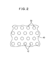
- the pattern 42 of the mask layer 40 is formed such that circular holes 44 are arranged at intersection points in an equilateral triangular lattice.
- the holes 44 which may have any diameters and intervals can be arranged with, for example, a diameter of each of the holes 44 in a range of 50 to 1000 nm and an interval between the holes 44 adjacent to each other in a range of 100 to 1000 nm.
- the nanocolumns 50 are grown through the pattern 42 of the mask layer 40 via the buffer 30.
- GaN is used for the nanocolumns 50.
- the nanocolumns 50 are grown corresponding to the pattern 42 so that dislocation density is made smaller than the case of growing them without the mask layer 40.
- the nanocolumns 50 can be formed into a cylindrical shape with an aspect ratio of 1 or more. Note that the nanocolumns 50 may be formed into any shapes other than a cylindrical shape as long as being formed into a columnar shape.
- the group III nitride semiconductor layer 10 is formed on the mask layer 40.
- the group III nitride semiconductor layer 10 includes an n-type layer 12, a multiple quantum well active layer 14, a p-type cladding layer 16 and a p-type contact layer 18 to be formed from the substrate 20 side in this order.
- the group III nitride semiconductor layer 10 is partially removed by etching to partially expose the n-type layer 12 and the exposed area is used for arranging an n-side electrode 60.
- a p-side electrode 62 is also formed on the p-type contact layer 18.
- the n-type layer 12 is formed of n-GaN obtained by doping a predetermined amount of n-type dopant (e.g. Si).
- the multiple quantum well active layer 14 also has a multiple quantum well structure formed by In x Ga 1-x N (0 ⁇ x ⁇ 1) / Al y Ga 1-y N (0 ⁇ y ⁇ 1).
- each of the p-type cladding layer 16 and the p-type contact layer 18 is formed by p-GaN obtained by doping a predetermined amount of p-type dopant (e.g. Mg).
- Layers from the n-type layer 12 to the p-type contact layer 18 are formed by epitaxial growth of a group III nitride semiconductor.
- a group III nitride semiconductor any layer structures can be employed in the group III nitride semiconductor layer 10 as long as including at least a first conductive layer, an active layer and a second conductive layer and allowing the active layer to emit light by recombined electrons and positive holes in response to voltage application to the first conductive layer and the second conductive layer.
- the n-side electrode 60 which is formed on the n-type layer 12 is made of, for example, Ni-Au and formed by the vacuum deposition method, sputtering method and CVD (Chemical Vapor Deposition) method or other methods.
- the p-side electrode 62 which is formed on the p-type contact layer 18 is made of, for example, ITO (Indium Tin Oxide) and formed by the vacuum deposition method, sputtering method and CVD (Chemical Vapor Deposition) method or other methods.
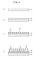
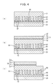
- Fig.3 and Fig.4 are a schematic cross sectional view of the LED element and Fig.5 is a flowchart of the method for manufacturing the LED element. Note that the LED element is illustrated by the unit of one element in Fig.3 and Fig.4 so as to correspond to Fig.1 for explanation, but it is actually provided in a wafer state before element separation and other elements are formed continuously to the left and right thereof.
- single crystal 6H-type SiC is generated in a bulk state containing donor impurities and acceptor impurities that were doped by the sublimation method.
- doping concentration of impurities in the SiC crystal can be controlled by adding impurity gas to atmospheric gas and adding an impurity element or a compound thereof to base powder at the growth of the crystal.
- the substrate 20 is fabricated by creating a bulk crystal of, for example, about 30 mm resulting from bulk growth by the sublimation method and passing through processes such as outer periphery grinding, slicing, surface grinding and surface polishing.
- the substrate 20 which may have any thicknesses is set to have a thickness of, for example, 250 ⁇ m.
- the buffer layer 30 is grown epitaxially on the surface 20 (i.e. buffer layer formation process S10 in Fig.5 ).
- the buffer layer 30 is formed to cover the entire surface on the substrate 20 by the sputtering method.
- the buffer layer 30 can also be formed by the MOCVD (Metal Organic Chemical Vapor Deposition) method, the MBE (Molecular Beam Epitaxy) method and the HVPE (Halide Vapor Phase Epitaxy) method or other methods.
- the buffer layer 30 can also be formed by the laser ablation method.
- the buffer layer 30 which may have any thicknesses is set to have a thickness of, for example, 10 to 200 nm.
- the mask layer 40 is formed above the substrate 20 on which the buffer layer 30 was formed (i.e. mask layer formation process S20 in Fig.5 ).
- the mask layer 40 is formed to cover the entire surface on the buffer layer 30 by the vacuum deposition method.
- the mask layer 40 which may have any thicknesses is set to have a thickness of, for example, 10 to 200 nm. With the thickness of this level, effects of inhibiting transmission of light emitted from an active layer by the mask layer 40 will be small. Moreover, if light is extracted by using the action of interference of light, it is unnecessary to take the above inhibiting effects into consideration and therefore the mask layer 40 may be set to be thick enough to achieve the action of interference.
- the pattern 44 is formed in the mask layer 40 by using the nanoimprint technique.
- the pattern 42 of the mask layer 40 is used to grow the nanocolumns 50 epitaxially (i.e. nanocolumn growth process S30 in Fig.5 ).
- the pattern 42 of the mask layer 40 is used to selectively grow the nanocolumns 50 on the buffer layer 30 by the MOCVD method.
- the MBE method and the HVPE method or other methods may also be used to grow the nanocolumns 50.
- the nanocolumns 50 which may have any heights are set to have a height of, for example, 500 nm.
- the nanocolumns 50 are selectively grown above the substrate 20, whereby dislocation density in the nanocolumns 50 is extremely small in comparison with a case of growing a semiconductor layer to cover the entire surface on the substrate 20.
- the group III nitride semiconductor layer 10 is grown (i.e. semiconductor layer growth process in Fig.5 ).
- the nanocolumns 50 and the group III nitride semiconductor layer 10 are grown continuously in the MOCVD device.
- the V/III ratio is preferably smaller in the nanocolumn growth process than in the semiconductor growth process.
- the V/III ratio can be less than 900 in the nanocolumn growth process. If the V/III ratio is too large at the growth of the nanocolumns, a semiconductor which is to be grown cannot be formed into a columnar shape.
- a semiconductor may be grown into crystals in an island state on the mask to be integrated with the nanocolumns or the nanocolumns may have various shapes.
- the multiple quantum well active layer 14 the p-type cladding layer 16 and the p-type contact layer 18 are grown sequentially from the mask layer 40 side as shown in Fig.4b .
- dislocation occurring in the inside is terminated in an area to be in contact with sidewalls of the nanocolumns 50, whereby dislocation density can be reduced.
- dislocation propagated from the nanocolumns 50 is extremely rare.
- the manufacturing process can be shortened in comparison with a case of growing the buffer layer 30 by the MOCVD device. Therefore, manufacturing costs of the light emitting element 1 can be reduced.
- the group III nitride semiconductor layer 10 of a good quality can be obtained. If the mask layer 40 which is amorphous is formed after formation of the nanocolumns 50 made of a group III nitride semiconductor, the surface of the nanocolumns 50 is deteriorated by the components of the mask layer 40 and the deteriorated nanocolumns 50 are used as a seed to grow the group III nitride semiconductor layer 10, wherein the group III nitride semiconductor layer 10 of a good quality is difficult to obtain.
- the mask layer 40 made of an amorphous material prevents the group III nitride semiconductor layer 10 formed on the mask layer 40 from being firmly connected to the mask layer 40. Therefore, if excessive stress occurs between the group III nitride semiconductor layer 10 and the mask layer 40, relative slippage of the group III nitride semiconductor layer 10 and the mask layer 40 is permissible. This will also contribute to reduction of dislocation density in the group III nitride semiconductor layer 10.
- each of layers in the group III nitride semiconductor layer 10 may have any thicknesses but can also be set such that, for example, the n-type layer 12 has a thickness of 3 ⁇ m, the multiple quantum well active layer 14 has a thickness of 100 nm, the p-type cladding layer 16 has a thickness of 80 nm, and the p-type contact layer 18 has a thickness of 10 nm.
- the group III nitride semiconductor layer 10 can be set to have a thickness of 3 ⁇ m or more.
- a mask made of photoresist is formed on the p-type contact layer 18 by using the photolithography technique and etching is made from the p-type contact layer 18 to the surface of the n-type layer 12, after which the mask is removed (i.e. etching process S50 in Fig.5 ). Therefore, a mesa part composed of a plurality of compound semiconductor layers including the n-type layer 12 to the p-type contact layer 18 is formed as shown in Fig.4c
- the vacuum deposition method and the photolithography technique are used to form the n-side electrode 60 and the p-side electrode 62 (i.e. electrode formation process S60 in Fig.5 ).
- the present embodiment uses different materials for the n-side electrode 60 and the p-side electrode 62, the n-side electrode 40 and the p-side electrode 62 can be formed simultaneously by using the same material.
- a heat treatment can be applied at a predetermined temperature under a predetermined atmosphere for a predetermined period of time in order to ensure ohmic contact and adhesiveness between each of the electrodes 60 and 62 and the group III nitride semiconductor layer 10. Thereafter, the completed device is divided into a plurality of the LED elements 1 by dicing and thus the LED element 1 is manufactured.
- ultraviolet light is emitted from the multiple quantum well active layer 14 in response to voltage application to the p-side electrode 62 and the n-side electrode 60. Then, ultraviolet light is converted into visible light by the substrate 20 and emitted to the outside.
- the nanocolumns 50 are selectively grown through the mask layer 40 and therefore reduction of dislocation density in the nanocolumns 50 themselves can be achieved.
- dislocation propagated from the nanocolumns 50 to the group III nitride semiconductor layer 10 formed on the mask layer 40 is significantly reduced to achieve reduction of dislocation density in the group III nitride semiconductor layer 10.
- Dislocation which occurred in the group III nitride semiconductor layer 10 at the growth of the group III nitride semiconductor layer 10 is terminated at the interface to the nanocolumns 50 and therefore not propagated upward. Accordingly, reduction of dislocation density in the group III nitride semiconductor 10 can be precisely achieved.
- the buffer layer 30 which includes Al prevents the group III nitride semiconductor and the substrate from fiercely reacting to each other at the interface therebetween as observed when, for example, GaN is grown directly on a substrate made of SiC or Si, so that the group III nitride semiconductor layer 10 can be precisely grown on the substrate 20.
- the nanocolumns 50 can be grown by using the mask layer 40 which was formed on the substrate 20 and the group III nitride semiconductor layer 10 can also be grown on the mask layer 40 as it is. Accordingly, a mask layer removal process which has been carried out in the conventional method is unnecessary and therefore reduction of manufacturing costs can be achieved.
- the buffer layer 30 and the nanocolumns 50 by the sputtering method, a growth process at a low temperature becomes possible to improve mass productivity.
- the buffer layer can be formed into a crystal structure of good quality with fewer defects than that formed by the MOCVD method or other methods.
- Applicable devices include, for example, electronic devices such as field effect transistors and bipolar transistors and solar cells or the like.
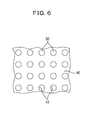
- nanocolumns 50 are arranged at intersection points in a triangular lattice according to the above embodiment, any changes can be made for the arrangement of the nanocolumns and, for example, arrangement at intersection points in a square lattice as shown in Fig.6 may also be applied.
- the present embodiment uses 6H-type SiC for the substrate 20, 4H-type Sic or 15R-type SiC may also be used as a matter of course and Si may also be used for the substrate 20.
- the substrate 20 may not need to have a fluorescence function and light of any colors may be emitted from the group III nitride semiconductor layer 10.
Landscapes
- Led Devices (AREA)
- Chemical & Material Sciences (AREA)
- Engineering & Computer Science (AREA)
- Nanotechnology (AREA)
Applications Claiming Priority (2)
| Application Number | Priority Date | Filing Date | Title |
|---|---|---|---|
| JP2010273209 | 2010-12-08 | ||
| PCT/JP2011/077240 WO2012077513A1 (fr) | 2010-12-08 | 2011-11-25 | Dispositif à semi-conducteur à nitrure du groupe iii et procédé de fabrication associé |
Publications (2)
| Publication Number | Publication Date |
|---|---|
| EP2571065A1 true EP2571065A1 (fr) | 2013-03-20 |
| EP2571065A4 EP2571065A4 (fr) | 2016-03-23 |
Family
ID=46207007
Family Applications (1)
| Application Number | Title | Priority Date | Filing Date |
|---|---|---|---|
| EP11847760.3A Withdrawn EP2571065A4 (fr) | 2010-12-08 | 2011-11-25 | Dispositif à semi-conducteur à nitrure du groupe iii et procédé de fabrication associé |
Country Status (5)
| Country | Link |
|---|---|
| US (1) | US9142619B2 (fr) |
| EP (1) | EP2571065A4 (fr) |
| JP (1) | JP5932664B2 (fr) |
| CN (1) | CN102959739B (fr) |
| WO (1) | WO2012077513A1 (fr) |
Cited By (13)
| Publication number | Priority date | Publication date | Assignee | Title |
|---|---|---|---|---|
| EP3131126A4 (fr) * | 2014-04-07 | 2017-10-11 | LG Innotek Co., Ltd. | Dispositif électroluminescent et système d'éclairage le comprenant |
| WO2019206844A1 (fr) * | 2018-04-22 | 2019-10-31 | Epinovatech Ab | Dispositif à film mince renforcé |
| WO2020165164A1 (fr) * | 2019-02-12 | 2020-08-20 | Osram Opto Semiconductors Gmbh | Composant optoélectronique |
| US11316165B2 (en) | 2020-01-24 | 2022-04-26 | Epinovatech Ab | Solid-state battery layer structure and method for producing the same |
| US11634824B2 (en) | 2021-06-09 | 2023-04-25 | Epinovatech Ab | Device for performing electrolysis of water, and a system thereof |
| US11652454B2 (en) | 2020-02-14 | 2023-05-16 | Epinovatech Ab | Monolithic microwave integrated circuit front-end module |
| US11695066B2 (en) | 2019-12-11 | 2023-07-04 | Epinovatech Ab | Semiconductor layer structure |
| WO2023138883A1 (fr) * | 2022-01-24 | 2023-07-27 | Ams-Osram International Gmbh | Procédé pour produire une pluralité de puces à semi-conducteur optoélectroniques et puce à semi-conducteur optoélectronique |
| US11955972B2 (en) | 2020-03-13 | 2024-04-09 | Epinovatech Ab | Field-programmable gate array device |
| US12027989B2 (en) | 2019-10-25 | 2024-07-02 | Epinovatech Ab | AC-DC converter circuit |
| US12395027B2 (en) | 2020-05-07 | 2025-08-19 | Epinovatech Ab | Induction machine |
| US12557325B2 (en) | 2020-05-29 | 2026-02-17 | Epinovatech Ab | Vertical HEMT and a method to produce a vertical HEMT |
| US12563670B2 (en) | 2021-05-10 | 2026-02-24 | Epinovatech Ab | Power converter device and a system comprising the same |
Families Citing this family (6)
| Publication number | Priority date | Publication date | Assignee | Title |
|---|---|---|---|---|
| JP2014076928A (ja) * | 2012-10-12 | 2014-05-01 | Waseda Univ | テンプレート基板 |
| FR2997551B1 (fr) * | 2012-10-26 | 2015-12-25 | Commissariat Energie Atomique | Procede de fabrication d'une structure semiconductrice et composant semiconducteur comportant une telle structure |
| CN103489974B (zh) * | 2013-08-30 | 2016-04-20 | 华灿光电股份有限公司 | 一种GaN基发光二极管外延片及其制作方法 |
| CN104638068B (zh) * | 2013-11-07 | 2018-08-24 | 上海蓝光科技有限公司 | 一种用于ⅲ-ⅴ族氮化物生长的衬底结构及其制备方法 |
| CN107611004B (zh) * | 2017-08-14 | 2020-01-31 | 南京大学 | 一种制备自支撑GaN衬底材料的方法 |
| CN112802930B (zh) * | 2021-04-15 | 2021-07-06 | 至芯半导体(杭州)有限公司 | Iii族氮化物衬底制备方法和半导体器件 |
Family Cites Families (17)
| Publication number | Priority date | Publication date | Assignee | Title |
|---|---|---|---|---|
| JPH07273367A (ja) * | 1994-04-01 | 1995-10-20 | Mitsubishi Cable Ind Ltd | 半導体基板の製造方法および発光素子の製造方法 |
| JP4153455B2 (ja) | 2003-11-28 | 2008-09-24 | 学校法人 名城大学 | 蛍光体および発光ダイオード |
| KR100646696B1 (ko) * | 2004-03-10 | 2006-11-23 | 주식회사 실트론 | 질화물 반도체 소자 및 그 제조방법 |
| DE112005000637T5 (de) | 2004-03-24 | 2008-06-26 | Meijo University Educational Foundation, Nagoya | Leuchtstoff und Leuchtdiode |
| JP2008511985A (ja) * | 2004-08-31 | 2008-04-17 | エージェンシー フォー サイエンス,テクノロジー アンド リサーチ | ナノ構造体及びそれを製造する方法 |
| KR100664986B1 (ko) * | 2004-10-29 | 2007-01-09 | 삼성전기주식회사 | 나노로드를 이용한 질화물계 반도체 소자 및 그 제조 방법 |
| JP4525500B2 (ja) | 2005-07-14 | 2010-08-18 | パナソニック電工株式会社 | 半導体発光素子およびそれを用いる照明装置ならびに半導体発光素子の製造方法 |
| KR101019941B1 (ko) * | 2006-03-10 | 2011-03-09 | 에스티씨. 유엔엠 | Gan 나노선의 펄스 성장 및 ⅲ 족 질화물 반도체 기판 물질과 디바이스에서의 어플리케이션 |
| CN101443887B (zh) * | 2006-03-10 | 2011-04-20 | Stc.Unm公司 | Gan纳米线的脉冲式生长及在族ⅲ氮化物半导体衬底材料中的应用和器件 |
| GB2436398B (en) * | 2006-03-23 | 2011-08-24 | Univ Bath | Growth method using nanostructure compliant layers and HVPE for producing high quality compound semiconductor materials |
| KR100767284B1 (ko) * | 2006-03-27 | 2007-10-17 | 학교법인 포항공과대학교 | 산화아연계 미세 구조물 및 그 제조방법 |
| JP5066825B2 (ja) | 2006-03-31 | 2012-11-07 | 新神戸電機株式会社 | 鉛蓄電池 |
| CN101681813B (zh) | 2007-01-12 | 2012-07-11 | 昆南诺股份有限公司 | 氮化物纳米线及其制造方法 |
| GB0702560D0 (en) * | 2007-02-09 | 2007-03-21 | Univ Bath | Production of Semiconductor devices |
| JP5097460B2 (ja) | 2007-06-26 | 2012-12-12 | パナソニック株式会社 | 化合物半導体素子およびそれを用いる照明装置ならびに化合物半導体素子の製造方法 |
| JP5112761B2 (ja) * | 2007-06-26 | 2013-01-09 | パナソニック株式会社 | 化合物半導体素子およびそれを用いる照明装置ならびに化合物半導体素子の製造方法 |
| JP5161759B2 (ja) | 2008-12-26 | 2013-03-13 | 富士通株式会社 | 化合物半導体装置の製造方法 |
-
2011
- 2011-11-25 JP JP2012547783A patent/JP5932664B2/ja not_active Expired - Fee Related
- 2011-11-25 WO PCT/JP2011/077240 patent/WO2012077513A1/fr not_active Ceased
- 2011-11-25 EP EP11847760.3A patent/EP2571065A4/fr not_active Withdrawn
- 2011-11-25 US US13/704,963 patent/US9142619B2/en not_active Expired - Fee Related
- 2011-11-25 CN CN201180031709.2A patent/CN102959739B/zh not_active Expired - Fee Related
Cited By (24)
| Publication number | Priority date | Publication date | Assignee | Title |
|---|---|---|---|---|
| EP3131126A4 (fr) * | 2014-04-07 | 2017-10-11 | LG Innotek Co., Ltd. | Dispositif électroluminescent et système d'éclairage le comprenant |
| US9911901B2 (en) | 2014-04-07 | 2018-03-06 | Lg Innotek Co., Ltd. | Light emitting device having buffer layer with graded composition |
| CN112020762A (zh) * | 2018-04-22 | 2020-12-01 | 艾普诺瓦泰克公司 | 增强型薄膜器件 |
| WO2019206844A1 (fr) * | 2018-04-22 | 2019-10-31 | Epinovatech Ab | Dispositif à film mince renforcé |
| US12009431B2 (en) | 2018-04-22 | 2024-06-11 | Epinovatech Ab | Reinforced thin-film device |
| CN112020762B (zh) * | 2018-04-22 | 2024-04-26 | 艾普诺瓦泰克公司 | 增强型薄膜器件 |
| EP4053880A1 (fr) * | 2018-04-22 | 2022-09-07 | Epinovatech AB | Dispositif à couche mince renforcée |
| US11469300B2 (en) | 2018-04-22 | 2022-10-11 | Epinovatech Ab | Reinforced thin-film semiconductor device and methods of making same |
| US12382656B2 (en) | 2018-04-22 | 2025-08-05 | Epinovatech Ab | Reinforced thin-film device |
| WO2020165164A1 (fr) * | 2019-02-12 | 2020-08-20 | Osram Opto Semiconductors Gmbh | Composant optoélectronique |
| US12027989B2 (en) | 2019-10-25 | 2024-07-02 | Epinovatech Ab | AC-DC converter circuit |
| US11695066B2 (en) | 2019-12-11 | 2023-07-04 | Epinovatech Ab | Semiconductor layer structure |
| US12148821B2 (en) | 2019-12-11 | 2024-11-19 | Epinovatech Ab | Semiconductor layer structure |
| US12456734B2 (en) | 2020-01-24 | 2025-10-28 | Epinovatech Ab | Solid-state battery layer structure and method for producing the same |
| US11316165B2 (en) | 2020-01-24 | 2022-04-26 | Epinovatech Ab | Solid-state battery layer structure and method for producing the same |
| US11652454B2 (en) | 2020-02-14 | 2023-05-16 | Epinovatech Ab | Monolithic microwave integrated circuit front-end module |
| US12068726B2 (en) | 2020-02-14 | 2024-08-20 | Epinovatech Ab | Monolithic microwave integrated circuit front-end module |
| US11955972B2 (en) | 2020-03-13 | 2024-04-09 | Epinovatech Ab | Field-programmable gate array device |
| US12355442B2 (en) | 2020-03-13 | 2025-07-08 | Epinovatech Ab | Field-programmable gate array device |
| US12395027B2 (en) | 2020-05-07 | 2025-08-19 | Epinovatech Ab | Induction machine |
| US12557325B2 (en) | 2020-05-29 | 2026-02-17 | Epinovatech Ab | Vertical HEMT and a method to produce a vertical HEMT |
| US12563670B2 (en) | 2021-05-10 | 2026-02-24 | Epinovatech Ab | Power converter device and a system comprising the same |
| US11634824B2 (en) | 2021-06-09 | 2023-04-25 | Epinovatech Ab | Device for performing electrolysis of water, and a system thereof |
| WO2023138883A1 (fr) * | 2022-01-24 | 2023-07-27 | Ams-Osram International Gmbh | Procédé pour produire une pluralité de puces à semi-conducteur optoélectroniques et puce à semi-conducteur optoélectronique |
Also Published As
| Publication number | Publication date |
|---|---|
| JPWO2012077513A1 (ja) | 2014-05-19 |
| CN102959739A (zh) | 2013-03-06 |
| US9142619B2 (en) | 2015-09-22 |
| EP2571065A4 (fr) | 2016-03-23 |
| JP5932664B2 (ja) | 2016-06-08 |
| CN102959739B (zh) | 2016-05-18 |
| US20130126907A1 (en) | 2013-05-23 |
| WO2012077513A1 (fr) | 2012-06-14 |
Similar Documents
| Publication | Publication Date | Title |
|---|---|---|
| US9142619B2 (en) | Group III nitride semiconductor device and method for manufacturing the same | |
| US12568717B2 (en) | Red LED and method of manufacture | |
| EP2017884A2 (fr) | Dispositifs comportant des couches à base de nitrure et des contacts enterrés et procédé de leur fabrication | |
| WO2007001098A1 (fr) | Nanostructure comprenant un puits quantique à base de nitrure et diode électroluminescente l'utilisant | |
| US12563866B2 (en) | LED and method of manufacture | |
| TW202211498A (zh) | Led裝置及製造方法 | |
| US20100012954A1 (en) | Vertical III-Nitride Light Emitting Diodes on Patterned Substrates with Embedded Bottom Electrodes | |
| KR20120138014A (ko) | 반도체 발광소자의 제조방법 | |
| WO2009002073A1 (fr) | Procédé de fabrication de dispositif semi-conducteur | |
| JP2008071773A (ja) | GaN系半導体発光ダイオードの製造方法 | |
| CN112802869A (zh) | 单片集成氮化物发光波长可调节的白光led及制备方法 | |
| KR101134493B1 (ko) | 발광 다이오드 및 이의 제조 방법 | |
| JP5946333B2 (ja) | Iii族窒化物半導体デバイス及びその製造方法 | |
| WO2007002607A2 (fr) | DISPOSITIFS ÉLECTRONIQUES ET/OU OPTOÉLECTRONIQUES DÉVELOPPÉS SUR DES SUBSTRATS AUTOPORTEURS DE GaN AVEC DES STRUCTURES D’ENTRETOISES EN GaN | |
| CN101728244A (zh) | 阻断半导体差排缺陷的方法 | |
| JP4548117B2 (ja) | 半導体発光素子の製造方法、集積型半導体発光装置の製造方法、画像表示装置の製造方法および照明装置の製造方法 | |
| KR20130055976A (ko) | 공극층을 갖는 발광 다이오드 및 그것을 제조하는 방법 | |
| KR20110135237A (ko) | 반도체 발광소자 및 그 제조방법 | |
| US12278257B2 (en) | Light Emitting Diode and method of forming a Light Emitting Diode | |
| KR100820836B1 (ko) | 발광 다이오드 제조방법 | |
| US20240079525A1 (en) | Efficient group iii-nitride led devices and method of fabrication | |
| KR100765722B1 (ko) | 나노 로드를 갖는 발광 소자 및 그의 제조 방법 | |
| KR101901932B1 (ko) | 이종 기판, 질화물 반도체 발광 소자 및 그 제조 방법 | |
| KR101910568B1 (ko) | 에피층과 성장 기판 분리 방법 및 이를 이용한 반도체 소자 | |
| US20200194619A1 (en) | Semiconductor devices with superlattice layers |
Legal Events
| Date | Code | Title | Description |
|---|---|---|---|
| PUAI | Public reference made under article 153(3) epc to a published international application that has entered the european phase |
Free format text: ORIGINAL CODE: 0009012 |
|
| 17P | Request for examination filed |
Effective date: 20121210 |
|
| AK | Designated contracting states |
Kind code of ref document: A1 Designated state(s): AL AT BE BG CH CY CZ DE DK EE ES FI FR GB GR HR HU IE IS IT LI LT LU LV MC MK MT NL NO PL PT RO RS SE SI SK SM TR |
|
| DAX | Request for extension of the european patent (deleted) | ||
| RA4 | Supplementary search report drawn up and despatched (corrected) |
Effective date: 20160218 |
|
| RIC1 | Information provided on ipc code assigned before grant |
Ipc: H01L 33/32 20100101ALN20160212BHEP Ipc: H01S 5/343 20060101ALI20160212BHEP Ipc: H01L 21/02 20060101ALI20160212BHEP Ipc: H01L 33/00 20100101AFI20160212BHEP Ipc: H01L 33/20 20100101ALI20160212BHEP Ipc: H01L 33/12 20100101ALN20160212BHEP |
|
| STAA | Information on the status of an ep patent application or granted ep patent |
Free format text: STATUS: THE APPLICATION IS DEEMED TO BE WITHDRAWN |
|
| 18D | Application deemed to be withdrawn |
Effective date: 20160920 |