EP2573716A2 - Circuit de sécurisation d'un dispositif sûr - Google Patents
Circuit de sécurisation d'un dispositif sûr Download PDFInfo
- Publication number
- EP2573716A2 EP2573716A2 EP12184989A EP12184989A EP2573716A2 EP 2573716 A2 EP2573716 A2 EP 2573716A2 EP 12184989 A EP12184989 A EP 12184989A EP 12184989 A EP12184989 A EP 12184989A EP 2573716 A2 EP2573716 A2 EP 2573716A2
- Authority
- EP
- European Patent Office
- Prior art keywords
- signal
- delay
- flip
- clock
- flop
- Prior art date
- Legal status (The legal status is an assumption and is not a legal conclusion. Google has not performed a legal analysis and makes no representation as to the accuracy of the status listed.)
- Granted
Links
Images


Classifications
-
- G—PHYSICS
- G06—COMPUTING OR CALCULATING; COUNTING
- G06K—GRAPHICAL DATA READING; PRESENTATION OF DATA; RECORD CARRIERS; HANDLING RECORD CARRIERS
- G06K19/00—Record carriers for use with machines and with at least a part designed to carry digital markings
- G06K19/06—Record carriers for use with machines and with at least a part designed to carry digital markings characterised by the kind of the digital marking, e.g. shape, nature, code
- G06K19/067—Record carriers with conductive marks, printed circuits or semiconductor circuit elements, e.g. credit or identity cards also with resonating or responding marks without active components
- G06K19/07—Record carriers with conductive marks, printed circuits or semiconductor circuit elements, e.g. credit or identity cards also with resonating or responding marks without active components with integrated circuit chips
- G06K19/073—Special arrangements for circuits, e.g. for protecting identification code in memory
- G06K19/07309—Means for preventing undesired reading or writing from or onto record carriers
- G06K19/07372—Means for preventing undesired reading or writing from or onto record carriers by detecting tampering with the circuit
Definitions
- Various exemplary embodiments disclosed herein relate generally to a secure device anti-tampering circuit.
- Smart cards are one example of secure devices in wide use.
- Contactless smart cards appeared several years ago in the form of electronic tags.
- Today contactless smart cards may be used in the fields of electronic ticketing, transport and access control. More recently they have started to be used for electronic payment transactions.
- a smartcard may provide security in the form of a hardware token. Encryption may be used in the smartcard to protect information from unauthorized disclosure. Plain text may be turned into cipher text via an encryption algorithm, and then decrypted back into plain text using the same method. In this way, the actual data exchange channel between smart card and reader may not be 'in the clear', and therefore may not be readable by an unauthorized third party or eavesdropper.
- a secure device anti-tampering circuit that detects and prevents physical attacks and/or reverse engineering of a secure device such as a smartcard.
- Various embodiments may also relate to an anti-tampering circuit for a secure device including: a signal delay detector; a clock delay detector; a clock duty cycle detector; and a protection unit that receives an error indication from the signal delay detector, clock delay detector, and the clock duty cycle detector, wherein the protection unit indicates tampering to a secure device upon receiving the error indication.
- an anti-tampering circuit for a secure device including: a delay unit that delays a signal from a chip wire, wherein the delay causes the signal on the chip wire to be timing critical; a first flip-flop configured to receive a delayed signal from the delay unit and a clock signal; a second flip-flop configured to receive a delayed signal from the delay unit and a delayed clock signal; and an XOR gate configured to receive output data from the first flip-flop and the second flip-flop wherein the XOR gate outputs an error indication if there is a difference between the output data of the first flip-flop and the output data of the second flip-flop.
- Various embodiments may also relate to a method for preventing tampering with a secure device including: delaying a signal on a chip wire in the secure device so that the signal on the chip wire becomes timing critical; loading data from the delayed signal in a first flip-flop; loading the data from the delayed signal in a second flip-flop; clocking the first flip-flop; clocking the second flip-flop after clocking the first flip-flop; comparing the clocked outputs from the first flip-flop and the second flip-flop; and outputting an error indication if the outputs from the first and second flip-flops are different.
- Various embodiments may also relate to method for preventing tampering with a secure device including: detecting a signal delay on a chip wire; detecting a delay in a clock signal using a low pass filter; detecting a change in shape of a clock signal using a delayed lock loop; and outputting an error indication if a signal delay on a chip wire is detected, a delay in a clock signal is detected, or a change in shape of a clock signal is detected.
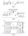
- Fig. 1 illustrates the parasitic effects on a signal on a chip wire.
- a chip wire 110 in a secure device has a parasitic resistance 120 and a parasitic capacitance 130.
- the parasitic resistance 120 and capacitance 130 form an RC circuit that introduces a delay on a signal carried on the chip wire 110. This delay is shown in the plot in Fig. 1 . This delay leads to a setup time that is the time it takes for the signal to reach its desired value.
- Fig. 2 illustrates the parasitic effects of a tap on a signal on a chip wire.
- the tap 210 includes a parasitic resistance 220 and a parasitic capacitance 230.
- the parasitic resistance 220 and capacitance 230 form an RC circuit that introduces a delay on a signal carried on the chip wire 210. This delay is in addition to the delay caused by the parasitic resistance 120 and capacitance 130 of the chip wire 110. These delays are shown in the plot in Fig. 2 .
- Fig. 3 illustrates a block diagram of a secure device including an embodiment of a secure device anti-tampering circuit.
- the secure device 300 may include an anti-tampering circuit 310, a controller 360, a memory 370, and an external interface 380.
- the anti-tampering circuit 310 may detect various types of tampering with the secure device.
- the controller 360 controls the overall operation of the secure device 300 and may include any standard type of controller, processor, etc. used in secure devices 300. Further, the controller 360 may carry out cryptographic functions.
- the memory 370 communicates with the controller 360.
- the memory may include identification and other information. Typically, the memory 370 in a secure device will have various safeguards to prevent unauthorized access to the information contained in the memory 370.
- the data stored in the memory 370 may be encrypted or unencrypted data. Further, cryptographic keys may be stored in the memory 370 as well.
- the external interface 380 may allow communication with devices external to the secure device 300. The external interface 380 may be either a contact or contactless interface.
- the anti-tampering circuit 310 may include a signal delay detector 320, a clock delay detector 330, a clock duty cycle detector 340, and a protection unit 350.
- the anti-tampering circuit 310 may determine if the secure device 300 has been tampered with, and if so may notify the controller 360 so that the controller may take action to prevent the tampering. Such actions may include, resetting the secure device 300, suspending operation of the secure device 300, or deleting cryptographic keys.
- parasitic resistance and capacitance on a chip wire 110 may cause a delay in the signal.
- the design of the circuit takes into account the delays that may be caused by the parasitic effects on the chip line 110. If the delay of the signal on the chip wire 110 becomes too great, then a setup timing error occurs. Therefore, a delay may be intentionally added to the signal on the chip wire so that it just avoids a setup timing error. In this situation, if the chip wire 110 is tapped, then the additional delay due to the parasitic effect of the tap will cause a setup timing error. Thus, the presence of a tap on the chip wire 110 may be detected.
- Fig. 4 illustrates the delay due to parasitic effects and a delay element on a signal on a chip wire.
- a delay element 440 may be placed on the chip wire 110 to add an additional amount of delay so that the signal one the chip wire 110 just meets the setup timing requirements during normal operation. This is illustrated in the plot in Fig. 4 .
- Fig. 5 illustrates an embodiment of a signal delay detector.
- the signal delay detector 320 may include a delay element 440, a first flip-flop 510, a second flip-flop 520, and XOR gate 530.
- the first flip-flop 510 may receive a delayed input signal from the delay unit 440 and a clock signal clk.
- the clock signal clk may trigger the operation of the first flip-flop 510.
- the second flip-flop 520 may also receive the delayed input signal from the delay unit 440 and a delayed clock signal clk_d.
- the delayed clock signal clk_d may trigger the operation of the second flip-flop 520.
- the delayed clock signal clk_d may cause the output of the second flip-flop 520 to be delayed relative to the output of the first flip-flop 510.
- the XOR gate 530 may receive the outputs of the first flip-flop 510 and the second flip-flop 520. The XOR gate 530 may produce an output that indicates whether the outputs of the first and second flip-flops 510, 520 are the same or different.
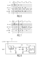
- Fig. 6 illustrates a timing diagram showing the operation of the signal delay detector in normal operation.
- the first flip-flop 510 may be by design timing critical. So for correct execution, the signal may need to be available within a certain limited timing window.
- the second flip-flop 520 that is triggered with delayed clock clk_d may be by design timing tolerant.
- the input signal including data D1 may be simultaneously input to both the first flip-flop 510 and the second flip-flop 520 as shown in Fig. 6 . Due to the delay that may be inserted by the delay element 440, the data D1 may arrive at the input of the first flip-flop 510 just within the allowed setup timing requirement. The data D1 may then be available on the output of the first flip-flop 510 in the next cycle. Simultaneously, the input data D1 may arrive at the input of the second flip-flop 520. Because the second flip-flop 520 may be triggered with the delayed clock clk_d, the input data D1 may arrive within the allowed setup timing requirement of the second flip-flop, and the data D1 may be available at the output of the second flip-flop 520.
- the outputs from the first flip-flop 510 and the second flip-flop 520 may be received by the XOR gate 530.
- the XOR gate 530 may compare the two outputs, if there is no difference, the output of the XOR gate 530 may be low.
- the logic of the XOR gate 530 may be inverted as well so that if there is no difference, the output of the XOR gate 530 may be high.
- the evaluation of the output of the XOR gate 530 may occur only when the delayed clock clk_d is high.
- Fig. 7 illustrates a timing diagram showing the operation of the signal delay detector when a tap is present on the chip wire 110.
- the input signal including input data D1 may be delayed beyond the allowed setup timing requirement due to the signal tap. Accordingly, the first flip-flop 510 may miss the timing deadline and may delay its output of data D1 to the next cycle.
- the second flip-flop 520 may be time tolerant, the second flip-flop 520 may receive the input data D1 on time, and therefore, the data D1 may be is still output as expected, resulting in difference in the outputs of the first flip-flop 510 and the second flip-flop 530. This difference may be determined by the XOR gate 530, and the XOR gate 530 may set an error flag. The error flag may indicate an unwanted activity.
- the controller 360 may reset the secure device 300, suspend operation of the secure device 300, or delete cryptographic keys.
- signal delay detectors 320 may be placed on these identified chip wires.
- the signal delay detector 320 may work only if the eavesdropper does not tap the input clock signal as well or slows the clock, which may make the design more delay tolerant allowing signal tapping.
- the clock delay detector 330 and the clock duty cycle detector 340 may be used to protect against this sort of attack.
- the clock delay detector 330 may measure the desired clock duty cycle and detect any frequency fluctuation beyond the allowed variation. This may be accomplished using an analog low pass filter inserted into the clock tree network.
- FIG. 8 illustrates a clock delay detector 330.
- the clock delay detector 330 may include a clock buffer 720, a resistor 730, a capacitor 740, and a voltage monitor 750. The resistor 730 and capacitor 740 form a low pass filter.
- the voltage monitor 750 may monitor Vopp and compare it to a threshold that is equal to the 1/2 Vipp + several % for the allowed frequency variation tolerance. If Vopp exceeds the threshold, then the voltage monitor 750 may output an error signal to the protection unit 350.
- Fig. 10 illustrates the output of the clock delay detector 330 when the clock is delayed. If the eavesdropper lowers the clock frequency of the smartcard, such that the period is twice the original period, Vopp may increase such that Vopp > (1/2*Vipp + several %). Accordingly, the voltage monitor 750 may detect that the threshold has been exceeded and may output an error signal to the protection unit 350.
- the clock duty cycle detector 340 may detect this difference in shape and signal an error if there is a variation.
- the clock duty cycle detector 340 may use a delay lock loop to compare the input clock with the clock that has been used in the digital design. If this comparison (e.g., by thresholding the difference between the time aligned clock signals) shows that the waveforms are not the same, then the clock duty cycle detector 340 may output an error signal to the protection unit 350.
- the secure device 300 may include only the signal delay detector 320 to identify attacks to the secure device 300.
- the secure device may additionally include either the clock delay detector 330 or the clock duty cycle detector 340 or both.
- the secure device 300 may include multiple signal delay detectors 320 to detect delays on multiple different chip wires in the secure device 300.
- the secure device 300 may include multiple signal delay detectors 320 and clock duty cycle detectors 340 to identify attacks on various clock wires in the secure device 300.
- the secure device may be a smart card, RFID tag, a NFC system, or any other secure device that needs to resist attacks.
Landscapes
- Engineering & Computer Science (AREA)
- Computer Hardware Design (AREA)
- Computer Security & Cryptography (AREA)
- General Engineering & Computer Science (AREA)
- Microelectronics & Electronic Packaging (AREA)
- Physics & Mathematics (AREA)
- General Physics & Mathematics (AREA)
- Theoretical Computer Science (AREA)
- Manipulation Of Pulses (AREA)
- Synchronisation In Digital Transmission Systems (AREA)
Applications Claiming Priority (1)
| Application Number | Priority Date | Filing Date | Title |
|---|---|---|---|
| US13/237,122 US8378710B1 (en) | 2011-09-20 | 2011-09-20 | Secure device anti-tampering circuit |
Publications (3)
| Publication Number | Publication Date |
|---|---|
| EP2573716A2 true EP2573716A2 (fr) | 2013-03-27 |
| EP2573716A3 EP2573716A3 (fr) | 2015-10-28 |
| EP2573716B1 EP2573716B1 (fr) | 2019-06-05 |
Family
ID=47357865
Family Applications (1)
| Application Number | Title | Priority Date | Filing Date |
|---|---|---|---|
| EP12184989.7A Active EP2573716B1 (fr) | 2011-09-20 | 2012-09-19 | Circuit de sécurisation d'un dispositif sûr. |
Country Status (3)
| Country | Link |
|---|---|
| US (1) | US8378710B1 (fr) |
| EP (1) | EP2573716B1 (fr) |
| CN (1) | CN103198347B (fr) |
Cited By (2)
| Publication number | Priority date | Publication date | Assignee | Title |
|---|---|---|---|---|
| WO2020144478A1 (fr) * | 2019-01-10 | 2020-07-16 | Arm Limited | Détection d'altération de largeur d'impulsion de signaux |
| US11621234B2 (en) | 2020-03-27 | 2023-04-04 | Semiconductor Components Industries, Llc | Chip tampering detector |
Families Citing this family (21)
| Publication number | Priority date | Publication date | Assignee | Title |
|---|---|---|---|---|
| US9235460B2 (en) | 2012-02-27 | 2016-01-12 | Altera Corporation | Methods and apparatus for automatic fault detection |
| US9046570B2 (en) * | 2012-08-03 | 2015-06-02 | Freescale Semiconductor, Inc. | Method and apparatus for limiting access to an integrated circuit (IC) |
| US9135431B2 (en) | 2013-07-26 | 2015-09-15 | Apple Inc. | Harmonic detector of critical path monitors |
| US9122891B2 (en) * | 2013-08-12 | 2015-09-01 | Microsoft Technology Licensing, Llc | Functional timing sensors |
| US9741231B2 (en) * | 2014-03-10 | 2017-08-22 | Nxp B.V. | Tamper/damage detection |
| US9542637B2 (en) * | 2014-12-31 | 2017-01-10 | Intermec, Inc. | RFID tag with anti-tamper assembly |
| US10050981B2 (en) * | 2015-05-04 | 2018-08-14 | Intel Corporation | Attack detection through signal delay monitoring |
| US9647653B2 (en) | 2015-06-04 | 2017-05-09 | Apple Inc. | Method for reduced power clock frequency monitoring |
| US9692403B2 (en) * | 2015-10-30 | 2017-06-27 | Texas Instruments Incorporated | Digital clock-duty-cycle correction |
| CN108075877B (zh) * | 2016-11-15 | 2022-04-29 | 华为技术有限公司 | 一种安全系统及终端芯片 |
| EP3340114B1 (fr) * | 2016-12-22 | 2020-09-30 | EM Microelectronic-Marin SA | Circuit rfid a deux frequences de communication muni d'une boucle d'inviolabilite |
| US9859890B1 (en) * | 2017-03-10 | 2018-01-02 | Bae Systems Information And Electronic Systems Integration Inc. | Method of preventing unauthorized use of analog and mixed-signal integrated circuits |
| US10289840B2 (en) * | 2017-06-02 | 2019-05-14 | Silicon Laboratories Inc. | Integrated circuit with tamper protection and method therefor |
| US10740499B2 (en) | 2018-03-12 | 2020-08-11 | Nuvoton Technology Corporation | Active shield portion serving as serial keypad |
| FR3084521B1 (fr) | 2018-07-25 | 2020-08-14 | Stmicroelectronics Rousset | Procede de protection d'un module de circuit integre et dispositif correspondant |
| FR3084520B1 (fr) | 2018-07-25 | 2020-08-14 | Stmicroelectronics Rousset | Procede de protection d'un circuit integre, et dispositif correspondant |
| FR3084492A1 (fr) | 2018-07-30 | 2020-01-31 | Stmicroelectronics (Rousset) Sas | Procede de detection d'une attaque par un faisceau de particules electriquement chargees sur un circuit integre, et circuit integre correspondant |
| FR3099259B1 (fr) | 2019-07-24 | 2021-08-13 | St Microelectronics Rousset | Procédé de protection de données stockées dans une mémoire, et circuit intégré correspondant |
| CN110443080B (zh) * | 2019-08-13 | 2021-03-30 | 艾体威尔电子技术(北京)有限公司 | 一种基于交互式查找表触发的回路网攻击检测系统及方法 |
| CN114586034B (zh) | 2019-11-19 | 2025-10-17 | 谷歌有限责任公司 | 时钟波动下的电压变化检测 |
| CN111800129B (zh) * | 2020-06-22 | 2022-11-11 | 华中科技大学 | 一种支持环境感知的puf单元、puf和混合puf |
Family Cites Families (16)
| Publication number | Priority date | Publication date | Assignee | Title |
|---|---|---|---|---|
| US5963267A (en) * | 1996-09-20 | 1999-10-05 | Thomson Consumer Electronics, Inc. | Delay correction circuit |
| JP2003296680A (ja) | 2002-03-29 | 2003-10-17 | Hitachi Ltd | データ処理装置 |
| KR100476892B1 (ko) | 2002-04-29 | 2005-03-17 | 삼성전자주식회사 | 데이터의 부정조작을 방지하는 방법 및 그것을 이용한데이터 처리 시스템 |
| US7634640B2 (en) | 2002-08-30 | 2009-12-15 | Infineon Technologies Ag | Data processing apparatus having program counter sensor |
| JP4122204B2 (ja) * | 2002-09-27 | 2008-07-23 | 松下電器産業株式会社 | 同期回路 |
| DE10326089B3 (de) * | 2003-06-10 | 2004-11-18 | Infineon Technologies Ag | Manipulationsüberwachung für eine Schaltung |
| FR2868577A1 (fr) | 2004-03-31 | 2005-10-07 | St Microelectronics Sa | Dispositif de detection d'attaque d'une puce de circuit integre |
| FR2911979A1 (fr) | 2007-01-29 | 2008-08-01 | St Microelectronics Sa | Procede et dispositif de verification de l'integrite d'un signal logique,notamment un signal d'horloge |
| FR2916560B1 (fr) * | 2007-05-21 | 2009-08-07 | Sagem Monetel Soc Par Actions | Cryptoprocesseur a protection de donnees amelioree |
| KR100911379B1 (ko) | 2007-06-14 | 2009-08-10 | 삼성전자주식회사 | 반도체 집적 회로의 해킹 검출기 및 그것의 검출 방법 |
| GB2452732A (en) | 2007-09-12 | 2009-03-18 | Seiko Epson Corp | Smart-card chip with organic conductive surface layer for detecting invasive attack |
| JP4388571B2 (ja) * | 2007-10-31 | 2009-12-24 | Okiセミコンダクタ株式会社 | 高速クロック検知回路 |
| JP2009147221A (ja) * | 2007-12-17 | 2009-07-02 | Renesas Technology Corp | 半導体装置 |
| FR2948795A1 (fr) | 2009-07-30 | 2011-02-04 | St Microelectronics Rousset | Detecteur d'injection de fautes dans un circuit integre |
| EP2290575A1 (fr) | 2009-08-31 | 2011-03-02 | Incard SA | Carte à circuit intégré comportant un processeur amélioré |
| KR101659840B1 (ko) * | 2010-03-11 | 2016-09-30 | 삼성전자주식회사 | 스큐드 게이트 타입 듀티 교정회로를 갖는 디지털 지연 동기 루프 및 그의 듀티 교정방법 |
-
2011
- 2011-09-20 US US13/237,122 patent/US8378710B1/en active Active
-
2012
- 2012-09-19 EP EP12184989.7A patent/EP2573716B1/fr active Active
- 2012-09-19 CN CN201210350049.0A patent/CN103198347B/zh active Active
Non-Patent Citations (1)
| Title |
|---|
| None |
Cited By (5)
| Publication number | Priority date | Publication date | Assignee | Title |
|---|---|---|---|---|
| WO2020144478A1 (fr) * | 2019-01-10 | 2020-07-16 | Arm Limited | Détection d'altération de largeur d'impulsion de signaux |
| US11022637B2 (en) | 2019-01-10 | 2021-06-01 | Arm Limited | Detection of pulse width tampering of signals |
| GB2595112A (en) * | 2019-01-10 | 2021-11-17 | Advanced Risc Mach Ltd | Detection of pulse width tampering of signals |
| GB2595112B (en) * | 2019-01-10 | 2023-01-04 | Advanced Risc Mach Ltd | Detection of pulse width tampering of signals |
| US11621234B2 (en) | 2020-03-27 | 2023-04-04 | Semiconductor Components Industries, Llc | Chip tampering detector |
Also Published As
| Publication number | Publication date |
|---|---|
| EP2573716A3 (fr) | 2015-10-28 |
| EP2573716B1 (fr) | 2019-06-05 |
| CN103198347B (zh) | 2015-09-23 |
| US8378710B1 (en) | 2013-02-19 |
| CN103198347A (zh) | 2013-07-10 |
Similar Documents
| Publication | Publication Date | Title |
|---|---|---|
| US8378710B1 (en) | Secure device anti-tampering circuit | |
| US9418250B2 (en) | Tamper detector with hardware-based random number generator | |
| EP2650813B1 (fr) | Dispositif et procédé de génération d'une clé d'identification | |
| US7205794B2 (en) | Microprocessor resistant to power analysis | |
| US8296845B2 (en) | Integrated circuits including reverse engineering detection using differences in signals | |
| US10044512B2 (en) | Decoupling of measuring the response time of a transponder and its authentication | |
| US20110299678A1 (en) | Secure means for generating a specific key from unrelated parameters | |
| KR100476892B1 (ko) | 데이터의 부정조작을 방지하는 방법 및 그것을 이용한데이터 처리 시스템 | |
| KR102515381B1 (ko) | 반복적인 사이드 채널 공격 대응책 | |
| CN111414605B (zh) | 嵌入式安全单元的解锁方法、装置、电子设备及存储介质 | |
| Mauw et al. | A PUF-based authentication protocol to address ticket-switching of RFID-tagged items | |
| KR101922931B1 (ko) | 보안 장치 및 그 동작 방법 | |
| JP5876364B2 (ja) | 半導体メモリ及びデータ読出方法 | |
| US20050041803A1 (en) | On-device random number generator | |
| JPWO2005027403A1 (ja) | 情報処理装置 | |
| US8430323B2 (en) | Electronic device and associated method | |
| US20060050876A1 (en) | Integrated circuit with coded security signal, security process, corresponding security device and signal coded using a dynamic key | |
| US8332662B2 (en) | Semiconductor integrated circuit and testing method thereof | |
| JP6280371B2 (ja) | 携帯可能電子装置、電子回路および端末 | |
| JP2000076402A (ja) | レスポンスタイムを可変化したicカード | |
| JP6110965B2 (ja) | 半導体メモリ | |
| CN205751076U (zh) | 一种随机数防篡改电路及安全装置 | |
| Tehranipoor | Security for RFID Tags | |
| HK1234854A1 (en) | Secure chip, and nonvolatile storage control device and method for same | |
| IDflex | Document Version: 1.0 Date: May 2, 2012 |
Legal Events
| Date | Code | Title | Description |
|---|---|---|---|
| PUAI | Public reference made under article 153(3) epc to a published international application that has entered the european phase |
Free format text: ORIGINAL CODE: 0009012 |
|
| AK | Designated contracting states |
Kind code of ref document: A2 Designated state(s): AL AT BE BG CH CY CZ DE DK EE ES FI FR GB GR HR HU IE IS IT LI LT LU LV MC MK MT NL NO PL PT RO RS SE SI SK SM TR |
|
| AX | Request for extension of the european patent |
Extension state: BA ME |
|
| 17P | Request for examination filed |
Effective date: 20140331 |
|
| PUAL | Search report despatched |
Free format text: ORIGINAL CODE: 0009013 |
|
| AK | Designated contracting states |
Kind code of ref document: A3 Designated state(s): AL AT BE BG CH CY CZ DE DK EE ES FI FR GB GR HR HU IE IS IT LI LT LU LV MC MK MT NL NO PL PT RO RS SE SI SK SM TR |
|
| AX | Request for extension of the european patent |
Extension state: BA ME |
|
| RIC1 | Information provided on ipc code assigned before grant |
Ipc: G06K 19/073 20060101AFI20150924BHEP |
|
| RBV | Designated contracting states (corrected) |
Designated state(s): AL AT BE BG CH CY CZ DE DK EE ES FI FR GB GR HR HU IE IS IT LI LT LU LV MC MK MT NL NO PL PT RO RS SE SI SK SM TR |
|
| STAA | Information on the status of an ep patent application or granted ep patent |
Free format text: STATUS: EXAMINATION IS IN PROGRESS |
|
| 17Q | First examination report despatched |
Effective date: 20180824 |
|
| GRAP | Despatch of communication of intention to grant a patent |
Free format text: ORIGINAL CODE: EPIDOSNIGR1 |
|
| STAA | Information on the status of an ep patent application or granted ep patent |
Free format text: STATUS: GRANT OF PATENT IS INTENDED |
|
| INTG | Intention to grant announced |
Effective date: 20190301 |
|
| GRAS | Grant fee paid |
Free format text: ORIGINAL CODE: EPIDOSNIGR3 |
|
| GRAA | (expected) grant |
Free format text: ORIGINAL CODE: 0009210 |
|
| STAA | Information on the status of an ep patent application or granted ep patent |
Free format text: STATUS: THE PATENT HAS BEEN GRANTED |
|
| AK | Designated contracting states |
Kind code of ref document: B1 Designated state(s): AL AT BE BG CH CY CZ DE DK EE ES FI FR GB GR HR HU IE IS IT LI LT LU LV MC MK MT NL NO PL PT RO RS SE SI SK SM TR |
|
| REG | Reference to a national code |
Ref country code: GB Ref legal event code: FG4D |
|
| REG | Reference to a national code |
Ref country code: CH Ref legal event code: EP |
|
| REG | Reference to a national code |
Ref country code: AT Ref legal event code: REF Ref document number: 1140743 Country of ref document: AT Kind code of ref document: T Effective date: 20190615 |
|
| REG | Reference to a national code |
Ref country code: IE Ref legal event code: FG4D |
|
| REG | Reference to a national code |
Ref country code: DE Ref legal event code: R096 Ref document number: 602012060671 Country of ref document: DE |
|
| REG | Reference to a national code |
Ref country code: NL Ref legal event code: MP Effective date: 20190605 |
|
| REG | Reference to a national code |
Ref country code: LT Ref legal event code: MG4D |
|
| PG25 | Lapsed in a contracting state [announced via postgrant information from national office to epo] |
Ref country code: AL Free format text: LAPSE BECAUSE OF FAILURE TO SUBMIT A TRANSLATION OF THE DESCRIPTION OR TO PAY THE FEE WITHIN THE PRESCRIBED TIME-LIMIT Effective date: 20190605 Ref country code: HR Free format text: LAPSE BECAUSE OF FAILURE TO SUBMIT A TRANSLATION OF THE DESCRIPTION OR TO PAY THE FEE WITHIN THE PRESCRIBED TIME-LIMIT Effective date: 20190605 Ref country code: ES Free format text: LAPSE BECAUSE OF FAILURE TO SUBMIT A TRANSLATION OF THE DESCRIPTION OR TO PAY THE FEE WITHIN THE PRESCRIBED TIME-LIMIT Effective date: 20190605 Ref country code: LT Free format text: LAPSE BECAUSE OF FAILURE TO SUBMIT A TRANSLATION OF THE DESCRIPTION OR TO PAY THE FEE WITHIN THE PRESCRIBED TIME-LIMIT Effective date: 20190605 Ref country code: NO Free format text: LAPSE BECAUSE OF FAILURE TO SUBMIT A TRANSLATION OF THE DESCRIPTION OR TO PAY THE FEE WITHIN THE PRESCRIBED TIME-LIMIT Effective date: 20190905 Ref country code: FI Free format text: LAPSE BECAUSE OF FAILURE TO SUBMIT A TRANSLATION OF THE DESCRIPTION OR TO PAY THE FEE WITHIN THE PRESCRIBED TIME-LIMIT Effective date: 20190605 Ref country code: SE Free format text: LAPSE BECAUSE OF FAILURE TO SUBMIT A TRANSLATION OF THE DESCRIPTION OR TO PAY THE FEE WITHIN THE PRESCRIBED TIME-LIMIT Effective date: 20190605 |
|
| PG25 | Lapsed in a contracting state [announced via postgrant information from national office to epo] |
Ref country code: RS Free format text: LAPSE BECAUSE OF FAILURE TO SUBMIT A TRANSLATION OF THE DESCRIPTION OR TO PAY THE FEE WITHIN THE PRESCRIBED TIME-LIMIT Effective date: 20190605 Ref country code: GR Free format text: LAPSE BECAUSE OF FAILURE TO SUBMIT A TRANSLATION OF THE DESCRIPTION OR TO PAY THE FEE WITHIN THE PRESCRIBED TIME-LIMIT Effective date: 20190906 Ref country code: LV Free format text: LAPSE BECAUSE OF FAILURE TO SUBMIT A TRANSLATION OF THE DESCRIPTION OR TO PAY THE FEE WITHIN THE PRESCRIBED TIME-LIMIT Effective date: 20190605 Ref country code: BG Free format text: LAPSE BECAUSE OF FAILURE TO SUBMIT A TRANSLATION OF THE DESCRIPTION OR TO PAY THE FEE WITHIN THE PRESCRIBED TIME-LIMIT Effective date: 20190905 |
|
| REG | Reference to a national code |
Ref country code: AT Ref legal event code: MK05 Ref document number: 1140743 Country of ref document: AT Kind code of ref document: T Effective date: 20190605 |
|
| PG25 | Lapsed in a contracting state [announced via postgrant information from national office to epo] |
Ref country code: NL Free format text: LAPSE BECAUSE OF FAILURE TO SUBMIT A TRANSLATION OF THE DESCRIPTION OR TO PAY THE FEE WITHIN THE PRESCRIBED TIME-LIMIT Effective date: 20190605 Ref country code: PT Free format text: LAPSE BECAUSE OF FAILURE TO SUBMIT A TRANSLATION OF THE DESCRIPTION OR TO PAY THE FEE WITHIN THE PRESCRIBED TIME-LIMIT Effective date: 20191007 Ref country code: SK Free format text: LAPSE BECAUSE OF FAILURE TO SUBMIT A TRANSLATION OF THE DESCRIPTION OR TO PAY THE FEE WITHIN THE PRESCRIBED TIME-LIMIT Effective date: 20190605 Ref country code: RO Free format text: LAPSE BECAUSE OF FAILURE TO SUBMIT A TRANSLATION OF THE DESCRIPTION OR TO PAY THE FEE WITHIN THE PRESCRIBED TIME-LIMIT Effective date: 20190605 Ref country code: CZ Free format text: LAPSE BECAUSE OF FAILURE TO SUBMIT A TRANSLATION OF THE DESCRIPTION OR TO PAY THE FEE WITHIN THE PRESCRIBED TIME-LIMIT Effective date: 20190605 Ref country code: EE Free format text: LAPSE BECAUSE OF FAILURE TO SUBMIT A TRANSLATION OF THE DESCRIPTION OR TO PAY THE FEE WITHIN THE PRESCRIBED TIME-LIMIT Effective date: 20190605 Ref country code: AT Free format text: LAPSE BECAUSE OF FAILURE TO SUBMIT A TRANSLATION OF THE DESCRIPTION OR TO PAY THE FEE WITHIN THE PRESCRIBED TIME-LIMIT Effective date: 20190605 |
|
| PG25 | Lapsed in a contracting state [announced via postgrant information from national office to epo] |
Ref country code: SM Free format text: LAPSE BECAUSE OF FAILURE TO SUBMIT A TRANSLATION OF THE DESCRIPTION OR TO PAY THE FEE WITHIN THE PRESCRIBED TIME-LIMIT Effective date: 20190605 Ref country code: IS Free format text: LAPSE BECAUSE OF FAILURE TO SUBMIT A TRANSLATION OF THE DESCRIPTION OR TO PAY THE FEE WITHIN THE PRESCRIBED TIME-LIMIT Effective date: 20191005 Ref country code: IT Free format text: LAPSE BECAUSE OF FAILURE TO SUBMIT A TRANSLATION OF THE DESCRIPTION OR TO PAY THE FEE WITHIN THE PRESCRIBED TIME-LIMIT Effective date: 20190605 |
|
| REG | Reference to a national code |
Ref country code: DE Ref legal event code: R097 Ref document number: 602012060671 Country of ref document: DE |
|
| PG25 | Lapsed in a contracting state [announced via postgrant information from national office to epo] |
Ref country code: TR Free format text: LAPSE BECAUSE OF FAILURE TO SUBMIT A TRANSLATION OF THE DESCRIPTION OR TO PAY THE FEE WITHIN THE PRESCRIBED TIME-LIMIT Effective date: 20190605 |
|
| PLBE | No opposition filed within time limit |
Free format text: ORIGINAL CODE: 0009261 |
|
| STAA | Information on the status of an ep patent application or granted ep patent |
Free format text: STATUS: NO OPPOSITION FILED WITHIN TIME LIMIT |
|
| PG25 | Lapsed in a contracting state [announced via postgrant information from national office to epo] |
Ref country code: PL Free format text: LAPSE BECAUSE OF FAILURE TO SUBMIT A TRANSLATION OF THE DESCRIPTION OR TO PAY THE FEE WITHIN THE PRESCRIBED TIME-LIMIT Effective date: 20190605 Ref country code: DK Free format text: LAPSE BECAUSE OF FAILURE TO SUBMIT A TRANSLATION OF THE DESCRIPTION OR TO PAY THE FEE WITHIN THE PRESCRIBED TIME-LIMIT Effective date: 20190605 |
|
| 26N | No opposition filed |
Effective date: 20200306 |
|
| PG25 | Lapsed in a contracting state [announced via postgrant information from national office to epo] |
Ref country code: MC Free format text: LAPSE BECAUSE OF FAILURE TO SUBMIT A TRANSLATION OF THE DESCRIPTION OR TO PAY THE FEE WITHIN THE PRESCRIBED TIME-LIMIT Effective date: 20190605 Ref country code: SI Free format text: LAPSE BECAUSE OF FAILURE TO SUBMIT A TRANSLATION OF THE DESCRIPTION OR TO PAY THE FEE WITHIN THE PRESCRIBED TIME-LIMIT Effective date: 20190605 |
|
| REG | Reference to a national code |
Ref country code: CH Ref legal event code: PL |
|
| PG25 | Lapsed in a contracting state [announced via postgrant information from national office to epo] |
Ref country code: LU Free format text: LAPSE BECAUSE OF NON-PAYMENT OF DUE FEES Effective date: 20190919 Ref country code: CH Free format text: LAPSE BECAUSE OF NON-PAYMENT OF DUE FEES Effective date: 20190930 Ref country code: LI Free format text: LAPSE BECAUSE OF NON-PAYMENT OF DUE FEES Effective date: 20190930 Ref country code: IE Free format text: LAPSE BECAUSE OF NON-PAYMENT OF DUE FEES Effective date: 20190919 |
|
| REG | Reference to a national code |
Ref country code: BE Ref legal event code: MM Effective date: 20190930 |
|
| PG25 | Lapsed in a contracting state [announced via postgrant information from national office to epo] |
Ref country code: BE Free format text: LAPSE BECAUSE OF NON-PAYMENT OF DUE FEES Effective date: 20190930 |
|
| GBPC | Gb: european patent ceased through non-payment of renewal fee |
Effective date: 20190919 |
|
| PG25 | Lapsed in a contracting state [announced via postgrant information from national office to epo] |
Ref country code: GB Free format text: LAPSE BECAUSE OF NON-PAYMENT OF DUE FEES Effective date: 20190919 |
|
| PG25 | Lapsed in a contracting state [announced via postgrant information from national office to epo] |
Ref country code: CY Free format text: LAPSE BECAUSE OF FAILURE TO SUBMIT A TRANSLATION OF THE DESCRIPTION OR TO PAY THE FEE WITHIN THE PRESCRIBED TIME-LIMIT Effective date: 20190605 |
|
| PG25 | Lapsed in a contracting state [announced via postgrant information from national office to epo] |
Ref country code: MT Free format text: LAPSE BECAUSE OF FAILURE TO SUBMIT A TRANSLATION OF THE DESCRIPTION OR TO PAY THE FEE WITHIN THE PRESCRIBED TIME-LIMIT Effective date: 20190605 Ref country code: HU Free format text: LAPSE BECAUSE OF FAILURE TO SUBMIT A TRANSLATION OF THE DESCRIPTION OR TO PAY THE FEE WITHIN THE PRESCRIBED TIME-LIMIT; INVALID AB INITIO Effective date: 20120919 |
|
| PG25 | Lapsed in a contracting state [announced via postgrant information from national office to epo] |
Ref country code: MK Free format text: LAPSE BECAUSE OF FAILURE TO SUBMIT A TRANSLATION OF THE DESCRIPTION OR TO PAY THE FEE WITHIN THE PRESCRIBED TIME-LIMIT Effective date: 20190605 |
|
| P01 | Opt-out of the competence of the unified patent court (upc) registered |
Effective date: 20230725 |
|
| PGFP | Annual fee paid to national office [announced via postgrant information from national office to epo] |
Ref country code: DE Payment date: 20250820 Year of fee payment: 14 |
|
| PGFP | Annual fee paid to national office [announced via postgrant information from national office to epo] |
Ref country code: FR Payment date: 20250820 Year of fee payment: 14 |