EP2575255A1 - Procédé et dispositif destinés à la détermination de la température d'un circuit semi-conducteur - Google Patents
Procédé et dispositif destinés à la détermination de la température d'un circuit semi-conducteur Download PDFInfo
- Publication number
- EP2575255A1 EP2575255A1 EP12182959A EP12182959A EP2575255A1 EP 2575255 A1 EP2575255 A1 EP 2575255A1 EP 12182959 A EP12182959 A EP 12182959A EP 12182959 A EP12182959 A EP 12182959A EP 2575255 A1 EP2575255 A1 EP 2575255A1
- Authority
- EP
- European Patent Office
- Prior art keywords
- semiconductor switch
- gate
- temperature
- voltage
- determining
- Prior art date
- Legal status (The legal status is an assumption and is not a legal conclusion. Google has not performed a legal analysis and makes no representation as to the accuracy of the status listed.)
- Granted
Links
Images

Classifications
-
- G—PHYSICS
- G01—MEASURING; TESTING
- G01K—MEASURING TEMPERATURE; MEASURING QUANTITY OF HEAT; THERMALLY-SENSITIVE ELEMENTS NOT OTHERWISE PROVIDED FOR
- G01K7/00—Measuring temperature based on the use of electric or magnetic elements directly sensitive to heat ; Power supply therefor, e.g. using thermoelectric elements
- G01K7/01—Measuring temperature based on the use of electric or magnetic elements directly sensitive to heat ; Power supply therefor, e.g. using thermoelectric elements using semiconducting elements having PN junctions
-
- H—ELECTRICITY
- H03—ELECTRONIC CIRCUITRY
- H03K—PULSE TECHNIQUE
- H03K17/00—Electronic switching or gating, i.e. not by contact-making and –breaking
- H03K17/08—Modifications for protecting switching circuit against overcurrent or overvoltage
- H03K17/081—Modifications for protecting switching circuit against overcurrent or overvoltage without feedback from the output circuit to the control circuit
- H03K17/0812—Modifications for protecting switching circuit against overcurrent or overvoltage without feedback from the output circuit to the control circuit by measures taken in the control circuit
- H03K17/08122—Modifications for protecting switching circuit against overcurrent or overvoltage without feedback from the output circuit to the control circuit by measures taken in the control circuit in field-effect transistor switches
-
- H—ELECTRICITY
- H03—ELECTRONIC CIRCUITRY
- H03K—PULSE TECHNIQUE
- H03K17/00—Electronic switching or gating, i.e. not by contact-making and –breaking
- H03K17/08—Modifications for protecting switching circuit against overcurrent or overvoltage
- H03K17/081—Modifications for protecting switching circuit against overcurrent or overvoltage without feedback from the output circuit to the control circuit
- H03K17/0812—Modifications for protecting switching circuit against overcurrent or overvoltage without feedback from the output circuit to the control circuit by measures taken in the control circuit
- H03K17/08128—Modifications for protecting switching circuit against overcurrent or overvoltage without feedback from the output circuit to the control circuit by measures taken in the control circuit in composite switches
-
- G—PHYSICS
- G01—MEASURING; TESTING
- G01K—MEASURING TEMPERATURE; MEASURING QUANTITY OF HEAT; THERMALLY-SENSITIVE ELEMENTS NOT OTHERWISE PROVIDED FOR
- G01K7/00—Measuring temperature based on the use of electric or magnetic elements directly sensitive to heat ; Power supply therefor, e.g. using thermoelectric elements
- G01K7/34—Measuring temperature based on the use of electric or magnetic elements directly sensitive to heat ; Power supply therefor, e.g. using thermoelectric elements using capacitative elements
- G01K7/346—Measuring temperature based on the use of electric or magnetic elements directly sensitive to heat ; Power supply therefor, e.g. using thermoelectric elements using capacitative elements for measuring temperature based on the time delay of a signal through a series of logical ports
-
- H—ELECTRICITY
- H03—ELECTRONIC CIRCUITRY
- H03K—PULSE TECHNIQUE
- H03K17/00—Electronic switching or gating, i.e. not by contact-making and –breaking
- H03K17/08—Modifications for protecting switching circuit against overcurrent or overvoltage
- H03K2017/0806—Modifications for protecting switching circuit against overcurrent or overvoltage against excessive temperature
Definitions
- Semiconductor switches are used inter alia, e.g. used for rectifying and inverting electrical voltages and currents, wherein usually a plurality of semiconductor switches for realizing a power converter are electrically connected together.
- the semiconductor switches are usually arranged on a substrate, which in turn is directly or indirectly connected to a heat sink.
- a semiconductor switch such as an IGBT (Insulated Gate Bipolar Transistor) or a MOSFET (Metal Oxide Semiconductor Field Effect Transistor) falls when turning on and off of the semiconductor switch in the semiconductor switch loss energy in the form of heat, which leads to heating of the semiconductor switch leads.
- the loss energy essentially accumulates on the so-called blocking layer of the semiconductor switch and leads to its temperature increase.
- the energy loss depends essentially on the frequency with which the semiconductor switch is turned on and off, as well as the electrical currents flowing through it during operation and the voltage applied across it.
- a plurality of semiconductor switches for realizing an electric valve must be electrically connected in series and / or in parallel.
- semiconductor switches such as eg IGBTs or MOSFETs, which have an electrical gate resistance integrated in the semiconductor switch, are known from the prior art.
- IGBTs or MOSFETs which have an electrical gate resistance integrated in the semiconductor switch.
- the application of an additional doped semiconductor layer to the already existing layers, which form the functional core of the semiconductor switch produces an electrical ohmic gate resistance, which as a rule has a value of a few ohms.
- silane SiH4
- SiO 2 insulator
- the polysilicon which has grown up in a layer is then doped.
- a metallization is applied to the doped polysilicon layer, which forms the externally accessible gate resistance terminal of the semiconductor switch.
- the second voltage is below the threshold voltage of the semiconductor switch.
- the second voltage is below the so-called threshold voltage of the semiconductor switch, i. is below the voltage threshold at which a significant collector current flows, i. the semiconductor switch begins to go into the conductive (on) state
- the determination of the time duration for determining the temperature of the semiconductor switch takes place below the so-called Miller plateau and the feedback of the collector-gate capacitance on the course of the gate-emitter Voltage does not affect the determination of the duration.
- a particularly accurate temperature determination of the temperature of the semiconductor switch is made possible.
- the semiconductor switch is designed as an IGBT or MOSFET, as these represent commercial semiconductor switch.
- circuit arrangement with a device according to the invention proves to be provided, wherein the circuit arrangement has a semiconductor switch which has an integrated electrical gate resistance, wherein the drive circuit of the device is electrically connected to the gate resistance terminal of the semiconductor switch via the external electrical resistance, wherein the time duration determination unit is connected to the gate resistance terminal of Semiconductor switch is electrically connected, as advantageous.
- FIG. 1 is in the form of an electrical block diagram of an inventive device 13 for determining the temperature T of a semiconductor switch 1, which has an integrated into the semiconductor switch 1 electrical gate resistance R Gint shown.
- the semiconductor switch 1 is formed in the embodiment as an IGBT and has the accessible from outside the semiconductor switch 1 for electrical connection of the semiconductor switch 1 with an external electrical component serving gate resistance terminal GA.
- the collector terminal CA By means of the collector terminal CA, the collector C of the semiconductor switch 1 can be electrically connected to the outside world and the emitter E of the semiconductor switch 1 can be electrically connected to the outside world by means of the emitter terminal EA, the emitter E being electrically connected to a load 2 in the exemplary embodiment is.
- the consisting of the gate G, emitter E, and collector C core of the semiconductor switch is in FIG.
- the semiconductor switch 1 represented in the form of the electrical symbol for an IGBT.
- the semiconductor switch 1 has an integrated in the semiconductor switch 1 electrical resistance ohmic resistor R Gint , which is electrically connected between the gate resistance terminal GA and the gate G.
- the gate resistor terminal GA is electrically connected to the gate G of the semiconductor switch 1 via the gate resistor R Gint .
- the semiconductor switch 1 which has the integrated gate resistance R Gint , is state of the art.
- the application of an additional doped semiconductor layer to the already present layers, which form the functional core of the semiconductor switch produces an electrical ohmic gate resistance, which as a rule has a value of a few ohms (eg 10 ohms).
- the parasitic gate-emitter capacitance C GE continues to be effective.
- the gate-emitter voltage U GE of a semiconductor switch is understood to mean the electrical voltage of the gate resistance terminal GA in relation to the emitter terminal EA of the semiconductor switch (see FIG. 1 ). With further increase of the gate-emitter voltage U GE the electrical resistance between collector and emitter is reduced to a minimum. The semiconductor switch 1 is then in the on state.
- the inventive device 13 has a drive circuit 3, which is designed to turn on the semiconductor switch by increasing the gate-emitter voltage U GE of the semiconductor switch 1 via a connected to the gate resistor terminal GA of the semiconductor switch 1 external electrical resistance R ext .
- the term "external" is expressed in the context of the present invention that the electrical resistance R ext is not part of the semiconductor switch 1.
- the drive circuit 3 is used to drive the semiconductor switch 1 and switches this, according to a pulse-shaped signal P, which is generated by a controller 10, on and off.
- the drive circuit 3 has a voltage source 11 which generates a control voltage U T as a function of the signal P.
- the drive circuit 3 and in particular the voltage source 11 is electrically connected via the external electrical resistance R ext to the gate resistance terminal GA of the semiconductor switch 1.
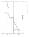
- the control voltage U T the negative voltage U a (see FIG. 2 ). Accordingly, in the stationary state, the gate-emitter voltage U GE, the negative voltage U a and the semiconductor switch 1 is turned off, ie, the electrical resistance between collector C and emitter E is high impedance.
- the controller 10 When the power switch is to be turned on, the controller 10 generates a value of "1" for the signal P. Upon receipt of the positive edge of the signal P, when the signal P goes from “0" to "1", the control voltage U jumps T from the negative voltage U a to the positive voltage U e . As a result of this, the parasitic gate-emitter capacitance C GE is charged via the electrically connected external resistor R ext and the integrated gate resistor R Gint until the voltage U e is applied across the gate-emitter capacitance C GE . The resulting course of the gate-emitter voltage U GE over the time t is in FIG. 2 shown.
- the timing of switching the control voltage U T from the negative voltage U a to the positive voltage U e represents the beginning E of the increase of the gate-emitter voltage and thus the beginning of the turn-on of the semiconductor switch 1.
- the gate-emitter voltage U GE increases until the threshold voltage U S is achieved rapidly. If the gate-emitter voltage U GE exceeds the threshold voltage U S then decreases electrical resistance between collector K and emitter E of the semiconductor switch 1 strong and the collector current I C begins to flow through the semiconductor switch 1 from the collector to the emitter and from there to the load 2. Due to the reaction of the collector-gate capacitance, which in the sake of clarity in FIG.
- the course of the gate-emitter voltage U GE in the region between the beginning E and the reaching of the threshold voltage U S is highly dependent on the electrical resistance of the integrated gate resistor R Gint .
- the greater the electrical resistance of the integrated gate resistor R Gint the flatter is the profile of the gate-emitter voltage U GE in the region between the beginning E and the reaching of the threshold voltage U S.
- the average slope of the gate-emitter voltage U GE in the region between the beginning E and the reaching of the threshold voltage U S decreases as the electrical resistance of the integrated gate resistor R Gint increases .
- the electrical resistance of the integrated gate resistor R Gint is temperature-dependent and increases with increasing temperature of the gate resistance R Gint and consequently with increasing temperature of the semiconductor switch .
- the gate-emitter voltage U GE in the region between the beginning E and the reaching of the threshold voltage U S increases the slower the higher the temperature of the semiconductor switch.
- This effect is used according to the invention to determine the temperature of the semiconductor switch. Since the integrated gate resistance R Gint is arranged in the immediate vicinity of the blocking layer of the semiconductor switch, at which a substantial part of the semiconductor switch's final energy loss is converted into heat, the gate resistance R Gint temperature and thus the gate resistance electrical resistance follows R Gint highly dynamic of the temperature of the junction of the semiconductor switch 1. Thus, a highly dynamic temperature determination of the semiconductor switch 1 is made possible by the invention.
- a time duration determination unit 14 which is required to determine the duration dt, which requires the gate-emitter voltage U GE during the increase of the gate-emitter voltage of the semiconductor switch, switches from a first voltage U 1 to a second one Increase voltage U 2 (see FIG. 2 ), is formed as an input.
- the Time duration determination unit 14 has, within the scope of the exemplary embodiment, a first limit value detector 4, a second limit value indicator 5, a counter 6 and a clock generator 15.
- the gate-emitter voltage U GE is supplied to the first and second limit detectors as input.
- the first limit value detector 4 When the gate-emitter voltage U GE reaches the predetermining first voltage U 1 , the first limit value detector 4 generates a signal S1 and transmits this to a counter 6.
- the second limit indicator 5 When the gate-emitter voltage U GE reaches the predetermining second voltage U 2 , the second limit indicator 5 generates a signal S2 and transmits this to a counter 6.
- the counter 6 receives a high-frequency equidistant clock F, which is generated by the clock 15. Upon receiving the signal S1, the counter 6 counts the number of clocks generated by the timer 15 since the reception of the signal S1 until it receives the signal S2.
- the counter thus determines the time duration dt, which requires the gate-emitter voltage U GE of the semiconductor switch 1 to increase from the first voltage U 1 to the second voltage U 2 , in the form of the number of the clock 15 since receiving the signal S1 to to generate the signal S2 generated clocks.
- the time duration dt is then transmitted as input to a temperature detection unit 7, which is designed to determine the temperature T of the semiconductor switch 1 on the basis of the determined time duration dt.
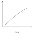
- the temperature determination unit 7 determines in the context of the embodiment, based on the temperature characteristic K of the semiconductor switch 1 (see FIG. 3 ), which determines the dependence of the temperature T of the semiconductor switch 1 on the time duration dt, which requires the gate-emitter voltage U GE of the semiconductor switch 1 to rise from the first voltage U 1 to the second voltage U 2 , the temperature T of Semiconductor switch 1.
- the temperature characteristic K of the semiconductor switch 1 can be determined empirically, for example.
- the determined temperature T of the semiconductor switch 1 is transmitted to a monitoring unit 8 as an input variable.
- the monitoring unit 8 is for turning off the semiconductor switch 1, when the determined temperature T of the semiconductor switch 1 reaches or exceeds a predetermined temperature limit T K is formed.
- the monitoring unit 8 generates in the context of the embodiment, when the determined temperature T of the semiconductor switch 1 reaches or exceeds a predetermined temperature limit T K , until a reset of the monitoring unit 8, a permanently pending switch-off signal A and transmits this as an input to the drive circuit 3, on receipt of the switch-off signal A as long as that Switch-off signal A is present until the negative voltage U a is generated independently of the pulse signal P and thus permanently switches off the semiconductor switch 1.
- the switch-off signal A is transmitted from the monitoring unit 8 to the controller 10, which indicates to the user a corresponding fault message.
- FIG. 1 only a single semiconductor switch shown and connected to the device 13 according to the invention.
- all or part of the semiconductor switch from which the valve is constructed be electrically connected to a respective associated device 13 according to the invention.
- the drive circuit 12 and the external resistor Rext can be part of a so-called driver circuit 12.
- semiconductor switches having no integrated gate resistance semiconductor switches having an integrated gate resistance, to realize the desired, e.g. power electronic circuit (e.g., rectifier, inverter, etc.).
- power electronic circuit e.g., rectifier, inverter, etc.
Landscapes
- Physics & Mathematics (AREA)
- General Physics & Mathematics (AREA)
- Electronic Switches (AREA)
- Power Conversion In General (AREA)
Applications Claiming Priority (1)
| Application Number | Priority Date | Filing Date | Title |
|---|---|---|---|
| DE201110083679 DE102011083679B3 (de) | 2011-09-29 | 2011-09-29 | Verfahren und Einrichtung zur Ermittlung der Temperatur eines Halbleiterschalters |
Publications (2)
| Publication Number | Publication Date |
|---|---|
| EP2575255A1 true EP2575255A1 (fr) | 2013-04-03 |
| EP2575255B1 EP2575255B1 (fr) | 2014-04-09 |
Family
ID=46831877
Family Applications (1)
| Application Number | Title | Priority Date | Filing Date |
|---|---|---|---|
| EP20120182959 Not-in-force EP2575255B1 (fr) | 2011-09-29 | 2012-09-04 | Procédé et dispositif destinés à la détermination de la température d'un circuit semi-conducteur |
Country Status (5)
| Country | Link |
|---|---|
| EP (1) | EP2575255B1 (fr) |
| CN (2) | CN203053594U (fr) |
| DE (1) | DE102011083679B3 (fr) |
| DK (1) | DK2575255T3 (fr) |
| ES (1) | ES2471871T3 (fr) |
Cited By (1)
| Publication number | Priority date | Publication date | Assignee | Title |
|---|---|---|---|---|
| WO2020064485A1 (fr) * | 2018-09-27 | 2020-04-02 | Thyssenkrupp Presta Ag | Mesure de température d'un élément disjoncteur à semi-conducteur |
Families Citing this family (12)
| Publication number | Priority date | Publication date | Assignee | Title |
|---|---|---|---|---|
| DE102011083679B3 (de) * | 2011-09-29 | 2012-09-27 | Semikron Elektronik Gmbh & Co. Kg Ip-Department | Verfahren und Einrichtung zur Ermittlung der Temperatur eines Halbleiterschalters |
| DE102012006009B4 (de) * | 2012-03-24 | 2024-06-13 | Volkswagen Aktiengesellschaft | Verfahren und Vorrichtung zur Bestimmung einer Sperrschichttemperatur eines Halbleiterbauelements |
| DE102014203655A1 (de) * | 2014-02-28 | 2015-09-03 | Siemens Aktiengesellschaft | Schaltungsanordnung und Verfahren zum Ansteuern eines Sperrschicht-Feldeffekttransistors |
| DE102014204648A1 (de) * | 2014-03-13 | 2015-09-17 | Zf Friedrichshafen Ag | Bestimmung einer IGBT-Temperatur |
| JP6750360B2 (ja) * | 2016-07-15 | 2020-09-02 | 富士電機株式会社 | 半導体装置 |
| EP3382357B1 (fr) * | 2017-03-31 | 2021-03-24 | Mitsubishi Electric R & D Centre Europe B.V. | Dispositif et procédé pour commander la température d'un module de puissance à puces multiples |
| DE102018204017A1 (de) * | 2018-03-16 | 2019-09-19 | Robert Bosch Gmbh | Verfahren und Vorrichtung zum Einstellen einer Totzeit von Schaltelementen einer Halbbrücke, und Wechselrichter |
| JP6958499B2 (ja) * | 2018-07-09 | 2021-11-02 | 三菱電機株式会社 | 半導体装置および電力変換装置 |
| DE102019119863B3 (de) | 2019-07-23 | 2020-06-25 | Semikron Elektronik Gmbh & Co. Kg | Schaltungseinrichtung mit einem Stromrichter und einem Kondensator |
| DE112021001992T5 (de) * | 2020-12-17 | 2023-01-12 | Fuji Electric Co., Ltd. | Temperaturmessverfahren und treibervorrichtung für spannungsgesteuertes halbleiterelement |
| DE102021210733A1 (de) | 2021-09-27 | 2023-03-30 | Robert Bosch Gesellschaft mit beschränkter Haftung | Verfahren und Schaltungsanordnungen zum Ermitteln einer Sperrschichttemperatur eines Halbleiterbauelements mit isoliertem Gate |
| DE102021210712A1 (de) | 2021-09-27 | 2023-03-30 | Robert Bosch Gesellschaft mit beschränkter Haftung | Verfahren und Schaltungsanordnung zum Ermitteln einer Sperrschichttemperatur eines Halbleiterbauelements mit isoliertem Gate |
Citations (2)
| Publication number | Priority date | Publication date | Assignee | Title |
|---|---|---|---|---|
| EP1947433A1 (fr) * | 2005-09-28 | 2008-07-23 | The Kansai Electric Power Co., Inc. | Procédé de mesure de la température d un dispositif semi-conducteur et appareil de mesure de la température d un dispositif semi-conducteur |
| DE102008063806A1 (de) * | 2007-12-26 | 2009-07-30 | Jansen, Uwe, Dipl.-Ing. | Temperaturerfassung für ein Halbleiterbauelement |
Family Cites Families (6)
| Publication number | Priority date | Publication date | Assignee | Title |
|---|---|---|---|---|
| SE512796C2 (sv) * | 1998-09-18 | 2000-05-15 | Ericsson Telefon Ab L M | Förfarande jämte anordning för att mäta temperatur i en halvledarkomponent |
| JP3861613B2 (ja) * | 2001-03-27 | 2006-12-20 | 日産自動車株式会社 | オンチップ温度検出装置 |
| JP5037368B2 (ja) * | 2008-01-11 | 2012-09-26 | アルパイン株式会社 | 温度検出装置及び方法、並びに回路 |
| JP5189929B2 (ja) * | 2008-08-19 | 2013-04-24 | ルネサスエレクトロニクス株式会社 | 半導体スイッチ制御装置 |
| DE102010029147B4 (de) * | 2010-05-20 | 2012-04-12 | Semikron Elektronik Gmbh & Co. Kg | Verfahren zur Ermittlung der Temperatur eines Leistungshalbleiters |
| DE102011083679B3 (de) * | 2011-09-29 | 2012-09-27 | Semikron Elektronik Gmbh & Co. Kg Ip-Department | Verfahren und Einrichtung zur Ermittlung der Temperatur eines Halbleiterschalters |
-
2011
- 2011-09-29 DE DE201110083679 patent/DE102011083679B3/de not_active Expired - Fee Related
-
2012
- 2012-09-04 DK DK12182959T patent/DK2575255T3/da active
- 2012-09-04 EP EP20120182959 patent/EP2575255B1/fr not_active Not-in-force
- 2012-09-04 ES ES12182959.2T patent/ES2471871T3/es active Active
- 2012-09-29 CN CN 201220510790 patent/CN203053594U/zh not_active Withdrawn - After Issue
- 2012-09-29 CN CN201210376118.5A patent/CN103033275B/zh not_active Expired - Fee Related
Patent Citations (2)
| Publication number | Priority date | Publication date | Assignee | Title |
|---|---|---|---|---|
| EP1947433A1 (fr) * | 2005-09-28 | 2008-07-23 | The Kansai Electric Power Co., Inc. | Procédé de mesure de la température d un dispositif semi-conducteur et appareil de mesure de la température d un dispositif semi-conducteur |
| DE102008063806A1 (de) * | 2007-12-26 | 2009-07-30 | Jansen, Uwe, Dipl.-Ing. | Temperaturerfassung für ein Halbleiterbauelement |
Cited By (2)
| Publication number | Priority date | Publication date | Assignee | Title |
|---|---|---|---|---|
| WO2020064485A1 (fr) * | 2018-09-27 | 2020-04-02 | Thyssenkrupp Presta Ag | Mesure de température d'un élément disjoncteur à semi-conducteur |
| US12139214B2 (en) | 2018-09-27 | 2024-11-12 | Thyssenkrupp Presta Ag | Temperature measurement of a power semiconductor switching element |
Also Published As
| Publication number | Publication date |
|---|---|
| DE102011083679B3 (de) | 2012-09-27 |
| ES2471871T3 (es) | 2014-06-27 |
| EP2575255B1 (fr) | 2014-04-09 |
| DK2575255T3 (da) | 2014-06-30 |
| CN103033275A (zh) | 2013-04-10 |
| CN103033275B (zh) | 2016-12-21 |
| CN203053594U (zh) | 2013-07-10 |
Similar Documents
| Publication | Publication Date | Title |
|---|---|---|
| EP2575255B1 (fr) | Procédé et dispositif destinés à la détermination de la température d'un circuit semi-conducteur | |
| DE102010064253B4 (de) | Halbleiterbauelement mit Detektion thermisch bedingter Fehler | |
| DE102014200946C5 (de) | Überlast-Überwachungsvorrichtung und Verfahren zur Überlast-Überwachung | |
| EP2692046B1 (fr) | Dispositif de commande d'un redresseur | |
| EP3711162B1 (fr) | Protection d'un transistor à effet de champ fonctionnant dans le mode de commutation contre un courant de surcharge | |
| DE102012216318A1 (de) | Halbleitervorrichtung | |
| EP3487022B1 (fr) | Dispositif de protection avec trajets de courant parallels ainsi que procédé de fonctionnement d'un tel dispositif de protection | |
| DE102014202717B3 (de) | System zur Kapazitätsbestimmung eines Zwischenkreiskondensators und Verfahren zum Ansteuern eines Wechselrichters | |
| EP3561981A1 (fr) | Procédé de réduction de montée en température dans un élément de commutation recommandable | |
| EP2565608B1 (fr) | Composant semi-conducteur de type puce | |
| DE102006029332A1 (de) | Motorsteuerung zur PWM-modulierten Steuerung eines Elektromotors | |
| WO2016091281A1 (fr) | Dispositif de limitation de puissance lors de la commutation d'une charge, agencement de circuit et procédé | |
| DE102013106801B4 (de) | Leistungshalbleiterschaltung | |
| EP3011651A1 (fr) | Circuit et système d'accumulation d'énergie | |
| DE102021208466B4 (de) | Trennschaltereinheit | |
| WO2016046021A1 (fr) | Procédé et dispositif de détermination de paramètres de fonctionnement d'éléments de commutation d'un convertisseur | |
| DE102012200234B4 (de) | Verfahren und Steuereinrichtung zur Steuerung der Ausschaltgeschwindigkeit eines Halbleiterschalters | |
| DE102012205209B4 (de) | Verfahren zur Ermittlung des Temperaturverlaufs eines auf einem Substrat angeordneten ersten Leistungshalbleiterschalters eines Leistungshalbleiterschaltermoduls und Leistungshalbleiterschaltermodul | |
| DE102016216508A1 (de) | Steuern eines Halbleiterschalters in einem Schaltbetrieb | |
| EP2203977A1 (fr) | Circuit de protection d'un élément de commutation avec détection de surintensité de courant et d'élévation de température | |
| DE102013108078B4 (de) | Leistungshalbleiterschaltung | |
| DE202016102848U1 (de) | Elektronischer Schutzschalter | |
| DE102019212654A1 (de) | Halbleitermodul und Leistungswandlervorrichtung | |
| DE102021127644A1 (de) | Verfahren zur Überwachung des Betriebs einer Stromrichtereinrichtung und Stromrichteranordnung | |
| JP6469910B1 (ja) | 過電圧保護回路 |
Legal Events
| Date | Code | Title | Description |
|---|---|---|---|
| PUAI | Public reference made under article 153(3) epc to a published international application that has entered the european phase |
Free format text: ORIGINAL CODE: 0009012 |
|
| AK | Designated contracting states |
Kind code of ref document: A1 Designated state(s): AL AT BE BG CH CY CZ DE DK EE ES FI FR GB GR HR HU IE IS IT LI LT LU LV MC MK MT NL NO PL PT RO RS SE SI SK SM TR |
|
| AX | Request for extension of the european patent |
Extension state: BA ME |
|
| 17P | Request for examination filed |
Effective date: 20131002 |
|
| RBV | Designated contracting states (corrected) |
Designated state(s): AL AT BE BG CH CY CZ DE DK EE ES FI FR GB GR HR HU IE IS IT LI LT LU LV MC MK MT NL NO PL PT RO RS SE SI SK SM TR |
|
| GRAP | Despatch of communication of intention to grant a patent |
Free format text: ORIGINAL CODE: EPIDOSNIGR1 |
|
| RIC1 | Information provided on ipc code assigned before grant |
Ipc: G01K 7/01 20060101ALI20131125BHEP Ipc: H03K 17/0812 20060101AFI20131125BHEP Ipc: H03K 17/08 20060101ALN20131125BHEP Ipc: G01K 7/34 20060101ALI20131125BHEP |
|
| INTG | Intention to grant announced |
Effective date: 20131212 |
|
| GRAS | Grant fee paid |
Free format text: ORIGINAL CODE: EPIDOSNIGR3 |
|
| GRAA | (expected) grant |
Free format text: ORIGINAL CODE: 0009210 |
|
| AK | Designated contracting states |
Kind code of ref document: B1 Designated state(s): AL AT BE BG CH CY CZ DE DK EE ES FI FR GB GR HR HU IE IS IT LI LT LU LV MC MK MT NL NO PL PT RO RS SE SI SK SM TR |
|
| REG | Reference to a national code |
Ref country code: GB Ref legal event code: FG4D Free format text: NOT ENGLISH |
|
| REG | Reference to a national code |
Ref country code: AT Ref legal event code: REF Ref document number: 661812 Country of ref document: AT Kind code of ref document: T Effective date: 20140415 Ref country code: CH Ref legal event code: EP |
|
| REG | Reference to a national code |
Ref country code: IE Ref legal event code: FG4D Free format text: LANGUAGE OF EP DOCUMENT: GERMAN |
|
| REG | Reference to a national code |
Ref country code: DE Ref legal event code: R096 Ref document number: 502012000570 Country of ref document: DE Effective date: 20140522 |
|
| REG | Reference to a national code |
Ref country code: CH Ref legal event code: NV Representative=s name: BRAUNPAT BRAUN EDER AG, CH |
|
| REG | Reference to a national code |
Ref country code: DK Ref legal event code: T3 Effective date: 20140626 |
|
| REG | Reference to a national code |
Ref country code: NL Ref legal event code: VDEP Effective date: 20140409 |
|
| REG | Reference to a national code |
Ref country code: LT Ref legal event code: MG4D |
|
| PG25 | Lapsed in a contracting state [announced via postgrant information from national office to epo] |
Ref country code: BG Free format text: LAPSE BECAUSE OF FAILURE TO SUBMIT A TRANSLATION OF THE DESCRIPTION OR TO PAY THE FEE WITHIN THE PRESCRIBED TIME-LIMIT Effective date: 20140709 Ref country code: NL Free format text: LAPSE BECAUSE OF FAILURE TO SUBMIT A TRANSLATION OF THE DESCRIPTION OR TO PAY THE FEE WITHIN THE PRESCRIBED TIME-LIMIT Effective date: 20140409 Ref country code: NO Free format text: LAPSE BECAUSE OF FAILURE TO SUBMIT A TRANSLATION OF THE DESCRIPTION OR TO PAY THE FEE WITHIN THE PRESCRIBED TIME-LIMIT Effective date: 20140709 Ref country code: GR Free format text: LAPSE BECAUSE OF FAILURE TO SUBMIT A TRANSLATION OF THE DESCRIPTION OR TO PAY THE FEE WITHIN THE PRESCRIBED TIME-LIMIT Effective date: 20140710 Ref country code: IS Free format text: LAPSE BECAUSE OF FAILURE TO SUBMIT A TRANSLATION OF THE DESCRIPTION OR TO PAY THE FEE WITHIN THE PRESCRIBED TIME-LIMIT Effective date: 20140809 Ref country code: LT Free format text: LAPSE BECAUSE OF FAILURE TO SUBMIT A TRANSLATION OF THE DESCRIPTION OR TO PAY THE FEE WITHIN THE PRESCRIBED TIME-LIMIT Effective date: 20140409 |
|
| PG25 | Lapsed in a contracting state [announced via postgrant information from national office to epo] |
Ref country code: LV Free format text: LAPSE BECAUSE OF FAILURE TO SUBMIT A TRANSLATION OF THE DESCRIPTION OR TO PAY THE FEE WITHIN THE PRESCRIBED TIME-LIMIT Effective date: 20140409 Ref country code: RS Free format text: LAPSE BECAUSE OF FAILURE TO SUBMIT A TRANSLATION OF THE DESCRIPTION OR TO PAY THE FEE WITHIN THE PRESCRIBED TIME-LIMIT Effective date: 20140409 Ref country code: PL Free format text: LAPSE BECAUSE OF FAILURE TO SUBMIT A TRANSLATION OF THE DESCRIPTION OR TO PAY THE FEE WITHIN THE PRESCRIBED TIME-LIMIT Effective date: 20140409 Ref country code: HR Free format text: LAPSE BECAUSE OF FAILURE TO SUBMIT A TRANSLATION OF THE DESCRIPTION OR TO PAY THE FEE WITHIN THE PRESCRIBED TIME-LIMIT Effective date: 20140409 Ref country code: SE Free format text: LAPSE BECAUSE OF FAILURE TO SUBMIT A TRANSLATION OF THE DESCRIPTION OR TO PAY THE FEE WITHIN THE PRESCRIBED TIME-LIMIT Effective date: 20140409 |
|
| PG25 | Lapsed in a contracting state [announced via postgrant information from national office to epo] |
Ref country code: PT Free format text: LAPSE BECAUSE OF FAILURE TO SUBMIT A TRANSLATION OF THE DESCRIPTION OR TO PAY THE FEE WITHIN THE PRESCRIBED TIME-LIMIT Effective date: 20140811 |
|
| REG | Reference to a national code |
Ref country code: DE Ref legal event code: R097 Ref document number: 502012000570 Country of ref document: DE |
|
| PG25 | Lapsed in a contracting state [announced via postgrant information from national office to epo] |
Ref country code: SK Free format text: LAPSE BECAUSE OF FAILURE TO SUBMIT A TRANSLATION OF THE DESCRIPTION OR TO PAY THE FEE WITHIN THE PRESCRIBED TIME-LIMIT Effective date: 20140409 Ref country code: RO Free format text: LAPSE BECAUSE OF FAILURE TO SUBMIT A TRANSLATION OF THE DESCRIPTION OR TO PAY THE FEE WITHIN THE PRESCRIBED TIME-LIMIT Effective date: 20140409 Ref country code: CZ Free format text: LAPSE BECAUSE OF FAILURE TO SUBMIT A TRANSLATION OF THE DESCRIPTION OR TO PAY THE FEE WITHIN THE PRESCRIBED TIME-LIMIT Effective date: 20140409 Ref country code: EE Free format text: LAPSE BECAUSE OF FAILURE TO SUBMIT A TRANSLATION OF THE DESCRIPTION OR TO PAY THE FEE WITHIN THE PRESCRIBED TIME-LIMIT Effective date: 20140409 |
|
| PLBE | No opposition filed within time limit |
Free format text: ORIGINAL CODE: 0009261 |
|
| STAA | Information on the status of an ep patent application or granted ep patent |
Free format text: STATUS: NO OPPOSITION FILED WITHIN TIME LIMIT |
|
| 26N | No opposition filed |
Effective date: 20150112 |
|
| REG | Reference to a national code |
Ref country code: DE Ref legal event code: R097 Ref document number: 502012000570 Country of ref document: DE Effective date: 20150112 |
|
| PG25 | Lapsed in a contracting state [announced via postgrant information from national office to epo] |
Ref country code: MC Free format text: LAPSE BECAUSE OF FAILURE TO SUBMIT A TRANSLATION OF THE DESCRIPTION OR TO PAY THE FEE WITHIN THE PRESCRIBED TIME-LIMIT Effective date: 20140409 Ref country code: LU Free format text: LAPSE BECAUSE OF FAILURE TO SUBMIT A TRANSLATION OF THE DESCRIPTION OR TO PAY THE FEE WITHIN THE PRESCRIBED TIME-LIMIT Effective date: 20140904 |
|
| REG | Reference to a national code |
Ref country code: IE Ref legal event code: MM4A |
|
| PG25 | Lapsed in a contracting state [announced via postgrant information from national office to epo] |
Ref country code: BE Free format text: LAPSE BECAUSE OF NON-PAYMENT OF DUE FEES Effective date: 20140930 |
|
| PG25 | Lapsed in a contracting state [announced via postgrant information from national office to epo] |
Ref country code: SI Free format text: LAPSE BECAUSE OF FAILURE TO SUBMIT A TRANSLATION OF THE DESCRIPTION OR TO PAY THE FEE WITHIN THE PRESCRIBED TIME-LIMIT Effective date: 20140409 |
|
| PG25 | Lapsed in a contracting state [announced via postgrant information from national office to epo] |
Ref country code: IE Free format text: LAPSE BECAUSE OF NON-PAYMENT OF DUE FEES Effective date: 20140904 |
|
| PG25 | Lapsed in a contracting state [announced via postgrant information from national office to epo] |
Ref country code: SM Free format text: LAPSE BECAUSE OF FAILURE TO SUBMIT A TRANSLATION OF THE DESCRIPTION OR TO PAY THE FEE WITHIN THE PRESCRIBED TIME-LIMIT Effective date: 20140409 |
|
| PG25 | Lapsed in a contracting state [announced via postgrant information from national office to epo] |
Ref country code: CY Free format text: LAPSE BECAUSE OF FAILURE TO SUBMIT A TRANSLATION OF THE DESCRIPTION OR TO PAY THE FEE WITHIN THE PRESCRIBED TIME-LIMIT Effective date: 20140409 Ref country code: MT Free format text: LAPSE BECAUSE OF FAILURE TO SUBMIT A TRANSLATION OF THE DESCRIPTION OR TO PAY THE FEE WITHIN THE PRESCRIBED TIME-LIMIT Effective date: 20140409 |
|
| PG25 | Lapsed in a contracting state [announced via postgrant information from national office to epo] |
Ref country code: HU Free format text: LAPSE BECAUSE OF FAILURE TO SUBMIT A TRANSLATION OF THE DESCRIPTION OR TO PAY THE FEE WITHIN THE PRESCRIBED TIME-LIMIT; INVALID AB INITIO Effective date: 20120904 Ref country code: TR Free format text: LAPSE BECAUSE OF FAILURE TO SUBMIT A TRANSLATION OF THE DESCRIPTION OR TO PAY THE FEE WITHIN THE PRESCRIBED TIME-LIMIT Effective date: 20140409 |
|
| REG | Reference to a national code |
Ref country code: FR Ref legal event code: PLFP Year of fee payment: 5 |
|
| PGFP | Annual fee paid to national office [announced via postgrant information from national office to epo] |
Ref country code: DK Payment date: 20160923 Year of fee payment: 5 Ref country code: FI Payment date: 20160921 Year of fee payment: 5 |
|
| REG | Reference to a national code |
Ref country code: FR Ref legal event code: PLFP Year of fee payment: 6 |
|
| REG | Reference to a national code |
Ref country code: DK Ref legal event code: EBP Effective date: 20170930 |
|
| PG25 | Lapsed in a contracting state [announced via postgrant information from national office to epo] |
Ref country code: FI Free format text: LAPSE BECAUSE OF NON-PAYMENT OF DUE FEES Effective date: 20170904 |
|
| REG | Reference to a national code |
Ref country code: CH Ref legal event code: PCAR Free format text: NEW ADDRESS: HOLEESTRASSE 87, 4054 BASEL (CH) |
|
| PG25 | Lapsed in a contracting state [announced via postgrant information from national office to epo] |
Ref country code: MK Free format text: LAPSE BECAUSE OF FAILURE TO SUBMIT A TRANSLATION OF THE DESCRIPTION OR TO PAY THE FEE WITHIN THE PRESCRIBED TIME-LIMIT Effective date: 20140409 |
|
| REG | Reference to a national code |
Ref country code: FR Ref legal event code: PLFP Year of fee payment: 7 |
|
| PG25 | Lapsed in a contracting state [announced via postgrant information from national office to epo] |
Ref country code: AL Free format text: LAPSE BECAUSE OF FAILURE TO SUBMIT A TRANSLATION OF THE DESCRIPTION OR TO PAY THE FEE WITHIN THE PRESCRIBED TIME-LIMIT Effective date: 20140409 |
|
| REG | Reference to a national code |
Ref country code: AT Ref legal event code: MM01 Ref document number: 661812 Country of ref document: AT Kind code of ref document: T Effective date: 20170904 |
|
| PG25 | Lapsed in a contracting state [announced via postgrant information from national office to epo] |
Ref country code: DK Free format text: LAPSE BECAUSE OF NON-PAYMENT OF DUE FEES Effective date: 20170930 |
|
| PG25 | Lapsed in a contracting state [announced via postgrant information from national office to epo] |
Ref country code: AT Free format text: LAPSE BECAUSE OF NON-PAYMENT OF DUE FEES Effective date: 20170904 |
|
| PGFP | Annual fee paid to national office [announced via postgrant information from national office to epo] |
Ref country code: IT Payment date: 20190920 Year of fee payment: 8 |
|
| PGFP | Annual fee paid to national office [announced via postgrant information from national office to epo] |
Ref country code: CH Payment date: 20190924 Year of fee payment: 8 |
|
| PGFP | Annual fee paid to national office [announced via postgrant information from national office to epo] |
Ref country code: ES Payment date: 20191023 Year of fee payment: 8 |
|
| REG | Reference to a national code |
Ref country code: CH Ref legal event code: PL |
|
| PG25 | Lapsed in a contracting state [announced via postgrant information from national office to epo] |
Ref country code: CH Free format text: LAPSE BECAUSE OF NON-PAYMENT OF DUE FEES Effective date: 20200930 Ref country code: LI Free format text: LAPSE BECAUSE OF NON-PAYMENT OF DUE FEES Effective date: 20200930 |
|
| PG25 | Lapsed in a contracting state [announced via postgrant information from national office to epo] |
Ref country code: IT Free format text: LAPSE BECAUSE OF NON-PAYMENT OF DUE FEES Effective date: 20200904 |
|
| REG | Reference to a national code |
Ref country code: ES Ref legal event code: FD2A Effective date: 20220114 |
|
| PG25 | Lapsed in a contracting state [announced via postgrant information from national office to epo] |
Ref country code: ES Free format text: LAPSE BECAUSE OF NON-PAYMENT OF DUE FEES Effective date: 20200905 |
|
| PGFP | Annual fee paid to national office [announced via postgrant information from national office to epo] |
Ref country code: GB Payment date: 20230921 Year of fee payment: 12 |
|
| PGFP | Annual fee paid to national office [announced via postgrant information from national office to epo] |
Ref country code: FR Payment date: 20230918 Year of fee payment: 12 Ref country code: DE Payment date: 20230930 Year of fee payment: 12 |
|
| REG | Reference to a national code |
Ref country code: DE Ref legal event code: R119 Ref document number: 502012000570 Country of ref document: DE |
|
| GBPC | Gb: european patent ceased through non-payment of renewal fee |
Effective date: 20240904 |
|
| PG25 | Lapsed in a contracting state [announced via postgrant information from national office to epo] |
Ref country code: DE Free format text: LAPSE BECAUSE OF NON-PAYMENT OF DUE FEES Effective date: 20250401 |
|
| PG25 | Lapsed in a contracting state [announced via postgrant information from national office to epo] |
Ref country code: GB Free format text: LAPSE BECAUSE OF NON-PAYMENT OF DUE FEES Effective date: 20240904 |
|
| PG25 | Lapsed in a contracting state [announced via postgrant information from national office to epo] |
Ref country code: FR Free format text: LAPSE BECAUSE OF NON-PAYMENT OF DUE FEES Effective date: 20240930 |