EP2582048B1 - System, das mindestens aus einer Anordung mit mindestens einem integrierten Schaltkreis besteht, bei dem diese integrierten Schaltkreise in Form einer Matrixarchitektur miteinander verbunden sind, und das mit mindestens einer optischen Verbindung ausgestattet ist - Google Patents
System, das mindestens aus einer Anordung mit mindestens einem integrierten Schaltkreis besteht, bei dem diese integrierten Schaltkreise in Form einer Matrixarchitektur miteinander verbunden sind, und das mit mindestens einer optischen Verbindung ausgestattet ist Download PDFInfo
- Publication number
- EP2582048B1 EP2582048B1 EP12188039.7A EP12188039A EP2582048B1 EP 2582048 B1 EP2582048 B1 EP 2582048B1 EP 12188039 A EP12188039 A EP 12188039A EP 2582048 B1 EP2582048 B1 EP 2582048B1
- Authority
- EP
- European Patent Office
- Prior art keywords
- optical
- integrated circuits
- input
- output
- integrated circuit
- Prior art date
- Legal status (The legal status is an assumption and is not a legal conclusion. Google has not performed a legal analysis and makes no representation as to the accuracy of the status listed.)
- Active
Links
Images







Classifications
-
- H—ELECTRICITY
- H03—ELECTRONIC CIRCUITRY
- H03K—PULSE TECHNIQUE
- H03K19/00—Logic circuits, i.e. having at least two inputs acting on one output; Inverting circuits
- H03K19/02—Logic circuits, i.e. having at least two inputs acting on one output; Inverting circuits using specified components
- H03K19/173—Logic circuits, i.e. having at least two inputs acting on one output; Inverting circuits using specified components using elementary logic circuits as components
- H03K19/177—Logic circuits, i.e. having at least two inputs acting on one output; Inverting circuits using specified components using elementary logic circuits as components arranged in matrix form
-
- H—ELECTRICITY
- H03—ELECTRONIC CIRCUITRY
- H03K—PULSE TECHNIQUE
- H03K19/00—Logic circuits, i.e. having at least two inputs acting on one output; Inverting circuits
- H03K19/02—Logic circuits, i.e. having at least two inputs acting on one output; Inverting circuits using specified components
- H03K19/173—Logic circuits, i.e. having at least two inputs acting on one output; Inverting circuits using specified components using elementary logic circuits as components
- H03K19/177—Logic circuits, i.e. having at least two inputs acting on one output; Inverting circuits using specified components using elementary logic circuits as components arranged in matrix form
- H03K19/17736—Structural details of routing resources
-
- H—ELECTRICITY
- H03—ELECTRONIC CIRCUITRY
- H03K—PULSE TECHNIQUE
- H03K19/00—Logic circuits, i.e. having at least two inputs acting on one output; Inverting circuits
- H03K19/02—Logic circuits, i.e. having at least two inputs acting on one output; Inverting circuits using specified components
- H03K19/173—Logic circuits, i.e. having at least two inputs acting on one output; Inverting circuits using specified components using elementary logic circuits as components
- H03K19/177—Logic circuits, i.e. having at least two inputs acting on one output; Inverting circuits using specified components using elementary logic circuits as components arranged in matrix form
- H03K19/17736—Structural details of routing resources
- H03K19/17744—Structural details of routing resources for input/output signals
Definitions
- the present invention relates to a system of at least one set comprising at least one integrated circuit, said integrated circuits being interconnected according to a matrix architecture of N rows and M columns of integrated circuits.
- Systems are known from at least one set of at least one integrated circuit, said integrated circuits being interconnected according to a matrix architecture of integrated circuits, in which the integrated circuits are interconnected by electrical connections, some of which type high speed fast serial interfaces, with a frequency well above 100 MHz.
- integrated circuit an electronic component performing a more or less complex electronic function, and often incorporating several types of elementary electronic components in a small volume box.
- Logic gates are the simplest digital integrated circuits, microprocessors and memories are among the most complex.
- integrated circuits dedicated to specific applications such as application specific integrated circuits or ASIC for "Application Specific Integrated Circuit” in English, in particular for signal processing; we then speak of digital signal processor or DSP for "Digital Signal Processor” in English language.
- a large family of integrated circuits is that of programmable logic components or FPGA for "Field Programmable Gaste Array" in English.
- hybrid module is meant a component integrating in the same housing a set of interconnected circuits, possibly made in different technologies, and able to process signals of different types (analog, radio-frequency, digital, optical).
- the processes are fragmented on a plurality of operators, which may be integrated circuits, circuits or hybrid modules, which are assembled on electronic cards within equipment.
- operators which may be integrated circuits, circuits or hybrid modules, which are assembled on electronic cards within equipment.
- integrated circuit is also used for hybrid modules.
- FIG. 1 illustrates such an example, wherein the system comprises sets of at least one integrated circuit C1, said integrated circuits being interconnected according to a matrix architecture of n1 lines Li and n2 columns Cj of integrated circuits C1, in this case identical.
- the system shown comprises 3n1 inputs or data channels and 4n2 outputs, because in this case the integrated circuits C1 each have 3 inputs and 4 outputs or processing channels.
- the document US 4811210 aims to implement different functions and different types of algorithms, on the same computer using a reconfigurable and parallel architecture.
- the proposed solution includes groups of processors integrating respectively a optical switch for configuring and modifying interconnections within the group and optical switches for exchanges between groups.
- This mode of hardware organization is not well suited to a matrix architecture in hardwired logic specific to an application, and in particular does not reduce its complexity and energy consumption.
- the document US 4696059 is intended to implement fast signal processing functions (programmable filter, word generator, programmable delay line), while the elementary delay functions are either insufficiently fast or non-adjustable.
- the proposed solution includes an optoelectronic switch and delay function groups, either electrical or optical.
- the elements, in optical technology, make it possible to realize the need for speed of the elementary delay function.
- the switch dynamically configures the connectivity between the primary inputs and the inputs / outputs of the delay functions, in order to synthesize different delay values, build filters or word generators.
- This architecture does not make it possible to build a complex matrix system comprising a large number of operators and integrated circuits and carrying out complex processes.
- An object of the invention is to overcome the problems mentioned above.
- a system of at least one set of at least one integrated circuit said integrated circuits being interconnected according to a matrix architecture of N rows and M columns of integrated circuits.
- a line receives at least one signal input, and a column provides at least one signal output.
- the interconnections between two integrated circuits of a line of the same set and the interconnections between two integrated circuits of a column of the same set are electric.
- An assembly of at least one integrated circuit comprises at least one input integrated circuit comprising at least one input of said set and at least one output integrated circuit comprising at least one output of said set, an input integrated circuit that can optionally be an output integrated circuit.
- the system includes at least one optical interconnection for connecting an input from a system line to a respective input of the input integrated circuits of the sets belonging to said line, or to connect a respective output of the output integrated circuits of the sets belonging to a column of the system to the system output of said column.
- Such a system makes it possible to significantly reduce the need for fast serial interfaces within the integrated circuits, and consequently the energy consumption and implementation complexity, in terms of the quantity of circuits and electronic cards. With a need for up to half the number of fast serial interfaces in integrated circuits, this system allows for better use of resources and integrated circuit input and output ports, and reduces the complexity of the equipment.
- optical links generally makes it possible to increase the bandwidth, and drastically reduce the weight and bulk of the links and connectors.
- an assembly of at least one integrated circuit is implanted in a single electronic card.
- the realization of such a system can be made from a plurality of copies of the same card, which facilitates the realization of the system and reduces its cost of implementation.
- an optical interconnection comprises an optical coupler and / or active optoelectronic coupling means and an optical link by an input integrated circuit input of the sets of a line or an output integrated circuit output of the sets. of a column.
- the optical links can simply be used to broadcast high-speed signals from one point to a plurality of points, and / or to combine a set of outputs from multiple integrated circuits, without significantly affecting the bit rate and the quality. signals to the interfaces.
- At least one line optical interconnection further comprises a test optical link.
- an optical link includes optical fiber.
- optical fiber makes it possible, among other things, to increase the bandwidth or the transmission distance, to guarantee good isolation between the different links, or to facilitate the physical implementation of the links.
- At least one line optical interconnection further comprises an optical amplifier.
- the power of the optical signal to be distributed by the outputs of an optical coupler can be adapted to the distribution need, in order to guarantee the transmission performance of the links.
- a plurality of line optical interconnects may be input connected by at least one optical switch, and / or a plurality of column optical interconnects may be outputted by at least one optical switch.
- At least one optical link is adapted to perform a wavelength division multiplexing.
- the system comprises at least one set of redundant integrated circuits provided with optical links.
- the system as described above can be adapted to perform a function of digital formation of antenna beams, and / or to perform a switching function.
- a processor comprising at least one system as previously described.
- a satellite comprising at least one processor as previously described embedded on board.
- a method of interconnecting at least one set of at least one integrated circuit according to a matrix architecture of n1 lines and n2 columns of integrated circuits, a line receiving at least one signal input, and a column providing at least one signal output, the interconnections between two integrated circuits of a line of the same set and the interconnections between two integrated circuits of a column of the same set being made electrically, and an assembly of at least one integrated circuit comprising at least one integrated circuit of input comprising at least one input of said set and at least one output integrated circuit comprising at least one output of said set, an input integrated circuit possibly being an output integrated circuit.
- At least one input of one line of the system is optically interconnected to a respective input of the input integrated circuits of the sets belonging to said line, or at least one output of a system column to a respective output of the systems. integrated circuit output of sets, belonging to said column.
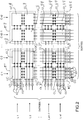
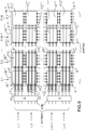
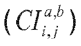
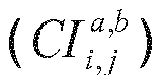
- the figure 2 schematically represents a system of at least one set E a, b , in the case E 1.1 , ..., E 1 , n 2/2 , ..., E n 1 / 2.1 , .. ., E n 1/2 , n 2/2 of at least one integrated circuit C I i , j at , b , in this case four integrated circuits C I 1.1 at , b , C I 1.2 at , b , C I 2.1 at , b , C I 2.2 at , b , (a integer varying from 1 to not 1 2 and b integer ranging from 1 to not 2 2 ) said integrated circuits C I i , j at , b (i integer varying from 1 to 2 and j integer ranging from 1 to 2) being interconnected according to a matrix architecture of n1 lines and n2 columns of integrated circuits C I i , j at , b .
- this example of four integrated circuits per set E a, b is in no way limiting, and the variations of the indices a and b of the sets E a, b depend on the number of integrated circuits per set E a, b .
- a line k of integrated circuits receives at least one signal input, in this case three inputs, and a column I of integrated circuits (I integer ranging from 1 to n2) provides at least one signal output, in this case four outputs.
- the interconnections between two integrated circuits of a line k of the same set E a, b , when this set comprises more than one integrated circuit per line, and the interconnections between two integrated circuits of a column I, when this set includes more than one integrated circuit per column, are electric.
- a set E a, b of at least one integrated circuit C I i , j at , b comprises at least one input integrated circuit, ie receiving input signals from outside the assembly, and at least one output integrated circuit, ie outputting output signals to the outside of the assembly.
- An input integrated circuit may optionally be simultaneously an output integrated circuit.
- the integrated circuits C I 1.1 at , b and C I 2.1 at , b are input integrated circuits
- integrated circuits C I 2.1 at , b and C I 2.2 at , b are output integrated circuits.
- the circuit C I 2.1 at , b is simultaneously an input integrated circuit and an output integrated circuit for the set E a, b .
- the system comprises at least one optical interconnection IO, in this case 3 ⁇ n1 + 4 ⁇ n2 optical interconnects, to connect a input of a system line to a respective input of the input integrated circuits of sets belonging to this line (3xn1 optical interconnections because in this example the integrated circuits have all three inputs belonging to optical interconnections), or to connect an output a column of the system at a respective output of the output integrated circuits of the sets belonging to this column (4xn2 optical interconnections because in this example the integrated circuits all have four outputs belonging to optical interconnections).
- optical interconnection IO in this case 3 ⁇ n1 + 4 ⁇ n2 optical interconnects
- the optical interconnections IO each comprise an optical coupler CO and an optical link LO by an input integrated circuit input of the sets of a line (in this case not 2 2 coupler optical links) or output IC output of the sets of a column in the present case not 1 2 coupler optical links).
- Optical coupler means a passive optical device comprising one or more optical input ports and one or more optical output ports, each of which distributes input signals to all of the output ports.
- an active optoelectronic coupling device comprising an electrical input port and a plurality of optical transmitters, each connected to an optical output port, and distributing the electrical input signal to the optical output port, may be used on transmission. set of optical output ports.
- an active optoelectronic coupling device may be used on reception, comprising a plurality of optical input ports each connected to an optical detector and an electrical output port, and collecting the optical input signals to the port of electrical output.
- the optical links LO may comprise optical fiber.
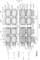
- the figure 3 represents a system similar to that of the figure 2 , wherein a set E a, b of at least one integrated circuit C I i , j at , b is included in a single electronic card CE a, b .
- the cards can be mass produced identically, and then easily connected according to a matrix architecture, for example only by optical interconnection IO.
- optical interconnection IO optical interconnection
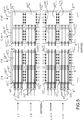
- the figure 4 represents a system similar to that of the figure 3 , in which the line optical interconnections IO further comprise a LOT optical test link, in this case to be able to observe the source data.
- the line optical interconnections IO further comprise a LOT optical test link, in this case to be able to observe the source data.
- only a fraction of these line optical interconnections 10 may be provided with a LOT optical test link.
- the presence of such a test link makes it possible to perform non-intrusive measurements on this line, which is not the case on high-speed electrical interconnections that are disturbed by the instrumentation.
- the optical line interconnections 10 may be provided with an additional optical test input, in this case to be able to inject test data. The presence of such a test link makes it possible to perform partial tests while the system is already assembled.
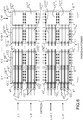
- the figure 5 represents a system similar to that of the figure 3 , wherein the optical interconnects are only along the lines of the matrix architecture, and the electronic boards each comprise a set of n1 integrated circuits arranged in a column.
- This configuration makes it possible to limit the electrical interconnections to the only interconnections internal to the electronic cards, and to carry out all the interconnections between cards by optical means.
- the figure 6 represents a system similar to that of the figure 5 , for a satellite beamforming processor, in which the optical interconnects are only along the lines of the matrix architecture.
- Each column of integrated circuits produces a set of beam outputs from 3xn1 inputs of a network antenna, for example in reception.
- This modular architecture makes it possible to simply increase the number of beams by adding electronic cards processing the same inputs.
- the figure 7 represents a matrix architecture system in which all the interconnections for all the integrated circuits, in rows and columns, are optical, considering that each set of integrated circuits comprises a single integrated circuit.
- This case corresponds to the generalization of the use of optical interfaces between integrated circuits in order to benefit from the capacity of diffusion and direct recombination of the optical signals.
- the system can, for example, be made on a single card.
- the figure 8 represents a system with matrix architecture similar to that of the figure 5 , wherein the optical interconnects are only along the lines of the matrix architecture, the electronic boards each comprise a set of n1 integrated circuits arranged in a column, and optical amplifiers AO to compensate the attenuation of the optical signals in the optical couplers.
- the figure 9 represents a system with matrix architecture similar to those of figures 5 and 8 , comprising optical input switches, for selecting, for reconfiguration purposes, the source inputs to be used.
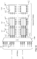
- the figure 10 is a matrix architecture system comprising an input COM optical switch for a satellite beamforming processor.
- the switch makes it possible to configure the association of the source data sets, originating from radiating elements in reception or transmission beams, to the sets of beam formers.
- the figure 11 represents a matrix architecture system comprising a plurality of COM optical switches in parallel for a satellite beam forming processor.
- paralleling a set of optical switches significantly reduces the complexity of each switch.
- the figure 12 represents a system with matrix architecture similar to that of the figure 4 , comprising COM optical switches between electronic cards for managing redundancies at the electronic cards CE a, b .
- This system makes it possible to substitute an unused card of the redundancy group RED for any failed electronic card.
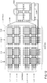
- the figure 13 represents a matrix architecture system comprising an inter-column COM optical switch for a satellite beamforming processor, the electronic boards CE a, b each comprising a set of n1 integrated circuits arranged in a column.
- the system includes a redundancy of r operator columns and a switching of these redundancies by full column (function). The failure of an operator penalizes the entire processing path (vertical) and generally the entire column. This redundancy switching mode consists of replacing the entire impacted column with an available redundant column.
- the optical distribution of the signals is suitable for switching redundant operators, using the diffusion capacity using optical couplers CO, and the implementation of optical switches COM.
- Switching redundancies can be achieved in different ways: by whole column, by processing, by circuit or electronic card, by line, or by data, the redundancies can be shared at different levels.
- the figure 13 illustrates redundancy switching by whole column (or whole function)
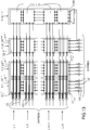
- the figure 14 illustrates a switching of pooled redundancies separately by line (or sub-function). Such an embodiment consists of having r redundant operators within each line of operators, with a redundancy switch specific to each line. For simplicity, the figure 14 presents a single horizontal operator-by-operator data channel, as well as a single vertical operator-processing channel. This mimic can be generalized with several horizontal data dissemination channels as well as several vertical processing channels per operator line.
- the redundant r operators receive by optical diffusion the data to be processed, like the Y nominal operators.
- the vertical processing channels also include optical links.
- Two-input and two-output CO optical couplers are associated with the nominal operators to broadcast the processed partial terms from the upstream line of either the nominal operator (of the same column) or a redundant operator at the destination the nominal operator and the redundancy group associated with the line.
- the redundancy group is switched using two COM optical switches, to switch the input and output processing channels. These optical switches perform switching between all the processing channels of the nominal operators and all the redundant operator processing channels.
- the redundancy capacity per line is overflowed when at least r + 1 faulty operators are concentrated on the same line. This system can therefore tolerate up to rxn1 operator failures.
- the figure 15 illustrates a variant of the figure 14 , switching mutualized redundancies separately by line (or sub-function) consisting of a homogeneous architecture of undifferentiated operators.
- This variant is more regular than the system of the figure 14 , without requiring optical couplers on the (vertical) treatment channels.
- the complexity of the optical switches COM is increased, while remaining very acceptable because of a better symmetry of the numbers of ports of entry and exit (r being lower than Y).
- the figure 16 illustrates another variant of figures 14 and 15 switching mutualized redundancies separately per line (or sub-function).
- the system of figure 15 can be modified to remove one of the two COM optical switches per line of operators.
- This variant consists of propagating Y + r treatment paths all along the chain vertical processing, with a COM optical switch at each line to define the connectivity with the operators of the next line.
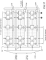
- the figure 17 illustrates a variant of the systems of figures 14 , 15 and 16 , switching mutualized redundancies separately by line (or sub-function).
- this variant consists in provisioning redundancy lines in addition to the nominal operator lines T which already integrate each r redundant operators.
- the redundancy capacity is increased by adding u redundant lines to the T lines of operators. This makes it possible to replace up to u lines of operators whose redundancy capacity has been overflowed (i.e. more than r operators failing).
- a COM input optical switch on the data side realizes the switching of the T input lines to all the T + u lines of operators.
- An operator line may be unused, either when it is an inactive redundancy, or when the redundancy capacity of this line is overflowed by an excess of failures.
- the (vertical) streams of partial terms from the upstream lines must traverse the inactive line transparently.
- One solution consists in locally broadcasting each stream of upstream partial term via a coupler to an input and two outputs diffusing towards each operator as well as to a so-called bypass way for "bypass" in English language.
- a COM switch with two inputs and an output downstream of the operator makes it possible to select either the processing output of the operator or the bypass channel at the input of the output switch Y + r: Y + r.
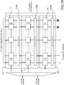
- the figure 18 illustrates a variant of the systems of figures 14 , 15 , 16 , and 17 switching mutualized redundancies separately per line (or sub-function).
- the optical couplers with one input and two outputs and the small two input COM optical switches and one output are replaced by an extension of the output switch capacity, to switch Y + r bypass channels in addition, ie a capacity of 2 (Y + r): 2 (Y + r).
- This solution provides the same redundancy efficiency as the previous variant, but has a simpler architecture, with higher capacity optical communications.
- optical interfaces of the figures 14 , 15 , 16 , 17 and 18 can carry either a data stream associated with a transceiver or element of high speed serial interface ("High Speed Serial Link transceiver" in English), or advantageously a multiplexing of data streams from a set of fast series transceivers located in the same operator (integrated circuit / hybrid module / digital card / equipment).
- WDM Wavelength Division Multiplexing
- wavelength division multiplexing WDM on the proposed schemes is particularly effective because it directly reduces the density of optical interconnections, and consequently the complexity of COM optical switches.
- the multiplexing concerns data streams distributed according to the same topology, which is the case for matrix digital architectures as defined, both for the dissemination of the data channels and for the distribution of the processing channels (partial terms).
Landscapes
- Physics & Mathematics (AREA)
- Mathematical Physics (AREA)
- Engineering & Computer Science (AREA)
- Computer Hardware Design (AREA)
- Computing Systems (AREA)
- General Engineering & Computer Science (AREA)
- Computer Networks & Wireless Communication (AREA)
- Optical Communication System (AREA)
Claims (12)
- System, bestehend aus mindestens zwei Anordnungen (Ea,b ), welche jeweils mindestens zwei integrierte Schaltkreise
 - eine Zeile (k) mindestens einen Signaleingang empfängt, und eine Spalte (l) mindestens einen Signalausgang bereitstellt, wobei die Verbindungen zwischen zwei integrierten Schaltkreisen einer Zeile (k) einer gleichen Anordnung und die Verbindungen zwischen zwei integrierten Schaltkreisen einer Spalte (l) einer gleichen Anordnung (Ea,b ) elektrisch sind,- wobei jede Anordnung (Ea,b ) mindestens einen der integrierten Schaltkreise, genannt Eingangs schaltkreis, beinhaltet, welcher mindestens einen optischen Eingang beinhaltet, und mindestens einen der integrierten Schaltkreise beinhaltet, genannt Ausgangsschaltkreis, welcher mindestens einen Ausgang der Anordnung beinhaltet, wobei ein integrierter Eingangs schaltkreis eventuell ein integrierter Ausgangsschaltkreis sein kann, wobei das System mindestens eine optische Verbindung (IO) zum Verbinden eines Eingangs einer Zeile mit Eingängen integrierter Eingangsschaltkreise der Anordnungen der Zeile (k) oder zum Verbinden von Ausgängen integrierter Ausgangsschaltkreise der Anordnungen einer Spalte (l) mit einem Ausgang der Spalte (l) beinhaltet; wobei eine optische Verbindung (IO) einen Optokoppler (CO) und/oder aktive optoelektronische Kopplungsmittel und einen optischen Link (LO) pro Eingang eines integrierten Eingangsschaltkreises der Anordnungen einer Zeile (k) oder pro Ausgang eines integrierten Ausgangsschaltkreises der Anordnungen einer Spalte (l) beinhaltet.
 - System nach Anspruch 1, bei welchem eine Anordnung (Ea,b ) in einer einzigen elektronischen Karte (CEa,b ) angeordnet ist.
- System nach einem der vorhergehenden Ansprüche, bei welchem mindestens eine optische Verbindung (IO) einer Zeile (k) zudem einen optischen Testlink (LOT) beinhaltet.
- System nach einem der vorhergehenden Ansprüche, bei welchem ein optischer Link (LO) Lichtwellenleiter beinhaltet.
- System nach einem der vorhergehenden Ansprüche, bei welchem mindestens eine optische Verbindung (IO) einer Zeile (k) zudem einen optischen Verstärker (AO) beinhaltet.
- System nach einem der vorhergehenden Ansprüche, bei welchem mehrere optische Verbindungen (IO) einer Zeile (k) am Eingang durch mindestens einen optischen Umschalter (COM) verbunden sind, und/oder mehrere optische Verbindungen (IO) einer Spalte (l) am Ausgang durch mindestens einen optischen Umschalter (COM) verbunden sind.
- System nach einem der vorhergehenden Ansprüche, bei welchem mindestens ein optischer Link (LO) geeignet ist, um ein Multiplexing durch Wellenlängenverteilung auszuführen.
- System nach einem der vorhergehenden Ansprüche, welches mindestens eine redundante Anordnung von integrierten Schaltkreisen beinhaltet, welche mit optischen Links (LO) versehen sind.
- System nach einem der vorhergehenden Ansprüche, welches geeignet ist, eine digitale Antennenstrahlformungsfunktion auszuführen.
- System nach einem der vorhergehenden Ansprüche, welches geeignet ist, eine Umschaltfunktion auszuführen.
- Prozessor, welcher mindestens ein System nach einem der vorhergehenden Ansprüche beinhaltet.
- Satellit, welcher mindestens einen an Bord mitgeführten Prozessor nach Anspruch 11 beinhaltet.
Applications Claiming Priority (1)
| Application Number | Priority Date | Filing Date | Title |
|---|---|---|---|
| FR1103141A FR2981477B1 (fr) | 2011-10-14 | 2011-10-14 | Systeme d'au moins un ensemble comprenant au moins un circuit integre, lesdits circuits integres etant interconnectes selon une architecture matricielle, muni d'au moins une interconnexion optique |
Publications (2)
| Publication Number | Publication Date |
|---|---|
| EP2582048A1 EP2582048A1 (de) | 2013-04-17 |
| EP2582048B1 true EP2582048B1 (de) | 2019-04-10 |
Family
ID=46970160
Family Applications (1)
| Application Number | Title | Priority Date | Filing Date |
|---|---|---|---|
| EP12188039.7A Active EP2582048B1 (de) | 2011-10-14 | 2012-10-10 | System, das mindestens aus einer Anordung mit mindestens einem integrierten Schaltkreis besteht, bei dem diese integrierten Schaltkreise in Form einer Matrixarchitektur miteinander verbunden sind, und das mit mindestens einer optischen Verbindung ausgestattet ist |
Country Status (5)
| Country | Link |
|---|---|
| US (1) | US20130094817A1 (de) |
| EP (1) | EP2582048B1 (de) |
| JP (1) | JP2013090337A (de) |
| CA (1) | CA2792172C (de) |
| FR (1) | FR2981477B1 (de) |
Families Citing this family (3)
| Publication number | Priority date | Publication date | Assignee | Title |
|---|---|---|---|---|
| CA3209399A1 (en) | 2021-02-24 | 2022-09-01 | Michael Thomas Pace | System and method for a digitally beamformed phased array feed |
| WO2023123286A1 (zh) * | 2021-12-30 | 2023-07-06 | 华为技术有限公司 | Wdm器件及制作方法,通信设备 |
| US12602298B2 (en) * | 2024-04-01 | 2026-04-14 | Google Llc | Self-repairable chip for silent data corruption issues |
Citations (1)
| Publication number | Priority date | Publication date | Assignee | Title |
|---|---|---|---|---|
| EP1569495A1 (de) * | 2004-02-26 | 2005-08-31 | Fujitsu Limited | Vorrichtung und System einer opto-elektronischen integrierten Schaltung und darauf basierendes Übertragungsverfahren |
Family Cites Families (10)
| Publication number | Priority date | Publication date | Assignee | Title |
|---|---|---|---|---|
| US4696059A (en) | 1984-03-07 | 1987-09-22 | Canadian Patents And Development Limited-Societe Canadienne Des Brevets Et D'exploitation Limitee | Reflex optoelectronic switching matrix |
| US4811210A (en) | 1985-11-27 | 1989-03-07 | Texas Instruments Incorporated | A plurality of optical crossbar switches and exchange switches for parallel processor computer |
| US5278548A (en) * | 1991-04-11 | 1994-01-11 | The United States Of America As Represented By The Secretary Of The Navy | Buffered feedthrough crossbar switch |
| AU2002246671A1 (en) * | 2000-12-13 | 2002-08-12 | Bae Systems Information And Electronic Systems Integration Inc. | Integrated circuit photonic signal matrix |
| US20040249964A1 (en) * | 2003-03-06 | 2004-12-09 | Thibault Mougel | Method of data transfer and apparatus therefor |
| US7921323B2 (en) * | 2004-05-11 | 2011-04-05 | L-3 Communications Integrated Systems, L.P. | Reconfigurable communications infrastructure for ASIC networks |
| US7444454B2 (en) | 2004-05-11 | 2008-10-28 | L-3 Communications Integrated Systems L.P. | Systems and methods for interconnection of multiple FPGA devices |
| US7889996B2 (en) * | 2007-12-21 | 2011-02-15 | Oracle America, Inc. | Optical-signal-path routing in a multi-chip system |
| FR2951040B1 (fr) * | 2009-10-06 | 2011-12-30 | Thales Sa | Antenne active reconfigurable a formation de faisceaux large bande par calcul |
| US8427368B1 (en) * | 2010-03-19 | 2013-04-23 | RKF Engineering Solutions, LLC | Amplitude calibration with pointing correction |
-
2011
- 2011-10-14 FR FR1103141A patent/FR2981477B1/fr not_active Expired - Fee Related
-
2012
- 2012-10-10 EP EP12188039.7A patent/EP2582048B1/de active Active
- 2012-10-12 US US13/650,795 patent/US20130094817A1/en not_active Abandoned
- 2012-10-12 CA CA2792172A patent/CA2792172C/en active Active
- 2012-10-15 JP JP2012228098A patent/JP2013090337A/ja active Pending
Patent Citations (1)
| Publication number | Priority date | Publication date | Assignee | Title |
|---|---|---|---|---|
| EP1569495A1 (de) * | 2004-02-26 | 2005-08-31 | Fujitsu Limited | Vorrichtung und System einer opto-elektronischen integrierten Schaltung und darauf basierendes Übertragungsverfahren |
Also Published As
| Publication number | Publication date |
|---|---|
| CA2792172C (en) | 2021-01-12 |
| CA2792172A1 (en) | 2013-04-14 |
| FR2981477A1 (fr) | 2013-04-19 |
| FR2981477B1 (fr) | 2014-05-23 |
| EP2582048A1 (de) | 2013-04-17 |
| US20130094817A1 (en) | 2013-04-18 |
| JP2013090337A (ja) | 2013-05-13 |
Similar Documents
| Publication | Publication Date | Title |
|---|---|---|
| EP2797167B1 (de) | Verteilte Zuführvorrichtung für Netz zur Bildung von Antennenstrahlen | |
| FR2750258A1 (fr) | Systeme de conformation de faisceau zonal reconfigurable pour une antenne embarquee sur un satellite en orbite et procede d'optimisation de la reconfiguration | |
| EP2562654A1 (de) | Ausweitbares Kommunikationsnetz auf Chip | |
| CA2821242C (fr) | Antenne et systeme d'antennes multifaisceaux comportant des sources compactes et systeme de telecommunication par satellite comportant au moins une telle antenne | |
| FR2729505A1 (fr) | Antenne multifaisceaux forte capacite a balayage electronique en emission | |
| EP2582048B1 (de) | System, das mindestens aus einer Anordung mit mindestens einem integrierten Schaltkreis besteht, bei dem diese integrierten Schaltkreise in Form einer Matrixarchitektur miteinander verbunden sind, und das mit mindestens einer optischen Verbindung ausgestattet ist | |
| CA2172013A1 (fr) | Dispositif d'alimentation d'une antenne multisources et multifaisceaux | |
| FR2811480A1 (fr) | Antenne de telecommunication destinee a couvrir une large zone terrestre | |
| EP2486675B1 (de) | Aktive umkonfigurierbare antenne zum erzeugen einer strahlenkeule durch rechnerisches ermitteln | |
| EP2481176B1 (de) | Passive multiportvorrichtung zur verteilung von optischen signalen | |
| CA2297298A1 (fr) | Modules de commutation, matrice de commutation comportant de tels modules, et reseau de commutation modulaire non bloquant comportant une telle matrice | |
| EP2989721B1 (de) | Kaskadierbare vorrichtung für digitalen mehrkanalempfang | |
| EP0749257B1 (de) | Schaltmatrix mit hoher Kapazität | |
| FR3013469A1 (fr) | Systeme d'interconnexion multifonctionnel pour meuble electronique et meuble comprenant un tel systeme | |
| FR3060248A1 (fr) | Reseau de communication embarque optique en anneau pour aeronef | |
| EP1052575A1 (de) | Übertragungsverfahren, Empfänger und verbundenes Netz | |
| EP1545035A1 (de) | Raum- und Frequenz-Crossconnect für einen Satelliten-Kommunikation-Verstärker und zugehöriger Verstärker und Satellit | |
| FR2988938A1 (fr) | Dispositifs de multiplexage dual en frequence | |
| FR3008265A1 (fr) | Systeme de production de faisceaux directifs multi liens simultanes | |
| EP1379100B1 (de) | Optischer Kreuzschienenverteiler mit granularer Architektur | |
| FR2735938A1 (fr) | Reseau de commutateurs c pour la connexion de canaux redondants | |
| FR3073294A1 (fr) | Dispositif de stimulation radioelectrique par panneau rayonnant autoreference | |
| EP1569369B1 (de) | Optisches Ringnetzwerk | |
| EP0982891A1 (de) | Vorrichtung zum Ein-Ausfügen eines optischen Wellenlängenmultiplexsignales | |
| EP2979363B1 (de) | Programmierbare verbindungsvorrichtung |
Legal Events
| Date | Code | Title | Description |
|---|---|---|---|
| PUAI | Public reference made under article 153(3) epc to a published international application that has entered the european phase |
Free format text: ORIGINAL CODE: 0009012 |
|
| AK | Designated contracting states |
Kind code of ref document: A1 Designated state(s): AL AT BE BG CH CY CZ DE DK EE ES FI FR GB GR HR HU IE IS IT LI LT LU LV MC MK MT NL NO PL PT RO RS SE SI SK SM TR |
|
| AX | Request for extension of the european patent |
Extension state: BA ME |
|
| 17P | Request for examination filed |
Effective date: 20131007 |
|
| RBV | Designated contracting states (corrected) |
Designated state(s): AL AT BE BG CH CY CZ DE DK EE ES FI FR GB GR HR HU IE IS IT LI LT LU LV MC MK MT NL NO PL PT RO RS SE SI SK SM TR |
|
| 17Q | First examination report despatched |
Effective date: 20160310 |
|
| STAA | Information on the status of an ep patent application or granted ep patent |
Free format text: STATUS: EXAMINATION IS IN PROGRESS |
|
| GRAP | Despatch of communication of intention to grant a patent |
Free format text: ORIGINAL CODE: EPIDOSNIGR1 |
|
| STAA | Information on the status of an ep patent application or granted ep patent |
Free format text: STATUS: GRANT OF PATENT IS INTENDED |
|
| INTG | Intention to grant announced |
Effective date: 20181205 |
|
| GRAS | Grant fee paid |
Free format text: ORIGINAL CODE: EPIDOSNIGR3 |
|
| GRAA | (expected) grant |
Free format text: ORIGINAL CODE: 0009210 |
|
| STAA | Information on the status of an ep patent application or granted ep patent |
Free format text: STATUS: THE PATENT HAS BEEN GRANTED |
|
| RAP1 | Party data changed (applicant data changed or rights of an application transferred) |
Owner name: THALES |
|
| AK | Designated contracting states |
Kind code of ref document: B1 Designated state(s): AL AT BE BG CH CY CZ DE DK EE ES FI FR GB GR HR HU IE IS IT LI LT LU LV MC MK MT NL NO PL PT RO RS SE SI SK SM TR |
|
| REG | Reference to a national code |
Ref country code: GB Ref legal event code: FG4D Free format text: NOT ENGLISH |
|
| REG | Reference to a national code |
Ref country code: CH Ref legal event code: EP Ref country code: AT Ref legal event code: REF Ref document number: 1120063 Country of ref document: AT Kind code of ref document: T Effective date: 20190415 |
|
| REG | Reference to a national code |
Ref country code: IE Ref legal event code: FG4D Free format text: LANGUAGE OF EP DOCUMENT: FRENCH |
|
| REG | Reference to a national code |
Ref country code: DE Ref legal event code: R096 Ref document number: 602012058771 Country of ref document: DE |
|
| REG | Reference to a national code |
Ref country code: NL Ref legal event code: MP Effective date: 20190410 |
|
| REG | Reference to a national code |
Ref country code: LT Ref legal event code: MG4D |
|
| REG | Reference to a national code |
Ref country code: AT Ref legal event code: MK05 Ref document number: 1120063 Country of ref document: AT Kind code of ref document: T Effective date: 20190410 |
|
| PG25 | Lapsed in a contracting state [announced via postgrant information from national office to epo] |
Ref country code: NL Free format text: LAPSE BECAUSE OF FAILURE TO SUBMIT A TRANSLATION OF THE DESCRIPTION OR TO PAY THE FEE WITHIN THE PRESCRIBED TIME-LIMIT Effective date: 20190410 |
|
| PG25 | Lapsed in a contracting state [announced via postgrant information from national office to epo] |
Ref country code: ES Free format text: LAPSE BECAUSE OF FAILURE TO SUBMIT A TRANSLATION OF THE DESCRIPTION OR TO PAY THE FEE WITHIN THE PRESCRIBED TIME-LIMIT Effective date: 20190410 Ref country code: AL Free format text: LAPSE BECAUSE OF FAILURE TO SUBMIT A TRANSLATION OF THE DESCRIPTION OR TO PAY THE FEE WITHIN THE PRESCRIBED TIME-LIMIT Effective date: 20190410 Ref country code: SE Free format text: LAPSE BECAUSE OF FAILURE TO SUBMIT A TRANSLATION OF THE DESCRIPTION OR TO PAY THE FEE WITHIN THE PRESCRIBED TIME-LIMIT Effective date: 20190410 Ref country code: NO Free format text: LAPSE BECAUSE OF FAILURE TO SUBMIT A TRANSLATION OF THE DESCRIPTION OR TO PAY THE FEE WITHIN THE PRESCRIBED TIME-LIMIT Effective date: 20190710 Ref country code: FI Free format text: LAPSE BECAUSE OF FAILURE TO SUBMIT A TRANSLATION OF THE DESCRIPTION OR TO PAY THE FEE WITHIN THE PRESCRIBED TIME-LIMIT Effective date: 20190410 Ref country code: PT Free format text: LAPSE BECAUSE OF FAILURE TO SUBMIT A TRANSLATION OF THE DESCRIPTION OR TO PAY THE FEE WITHIN THE PRESCRIBED TIME-LIMIT Effective date: 20190910 Ref country code: HR Free format text: LAPSE BECAUSE OF FAILURE TO SUBMIT A TRANSLATION OF THE DESCRIPTION OR TO PAY THE FEE WITHIN THE PRESCRIBED TIME-LIMIT Effective date: 20190410 Ref country code: LT Free format text: LAPSE BECAUSE OF FAILURE TO SUBMIT A TRANSLATION OF THE DESCRIPTION OR TO PAY THE FEE WITHIN THE PRESCRIBED TIME-LIMIT Effective date: 20190410 |
|
| PG25 | Lapsed in a contracting state [announced via postgrant information from national office to epo] |
Ref country code: PL Free format text: LAPSE BECAUSE OF FAILURE TO SUBMIT A TRANSLATION OF THE DESCRIPTION OR TO PAY THE FEE WITHIN THE PRESCRIBED TIME-LIMIT Effective date: 20190410 Ref country code: RS Free format text: LAPSE BECAUSE OF FAILURE TO SUBMIT A TRANSLATION OF THE DESCRIPTION OR TO PAY THE FEE WITHIN THE PRESCRIBED TIME-LIMIT Effective date: 20190410 Ref country code: BG Free format text: LAPSE BECAUSE OF FAILURE TO SUBMIT A TRANSLATION OF THE DESCRIPTION OR TO PAY THE FEE WITHIN THE PRESCRIBED TIME-LIMIT Effective date: 20190710 Ref country code: GR Free format text: LAPSE BECAUSE OF FAILURE TO SUBMIT A TRANSLATION OF THE DESCRIPTION OR TO PAY THE FEE WITHIN THE PRESCRIBED TIME-LIMIT Effective date: 20190711 Ref country code: LV Free format text: LAPSE BECAUSE OF FAILURE TO SUBMIT A TRANSLATION OF THE DESCRIPTION OR TO PAY THE FEE WITHIN THE PRESCRIBED TIME-LIMIT Effective date: 20190410 |
|
| PG25 | Lapsed in a contracting state [announced via postgrant information from national office to epo] |
Ref country code: IS Free format text: LAPSE BECAUSE OF FAILURE TO SUBMIT A TRANSLATION OF THE DESCRIPTION OR TO PAY THE FEE WITHIN THE PRESCRIBED TIME-LIMIT Effective date: 20190810 Ref country code: AT Free format text: LAPSE BECAUSE OF FAILURE TO SUBMIT A TRANSLATION OF THE DESCRIPTION OR TO PAY THE FEE WITHIN THE PRESCRIBED TIME-LIMIT Effective date: 20190410 |
|
| REG | Reference to a national code |
Ref country code: DE Ref legal event code: R097 Ref document number: 602012058771 Country of ref document: DE |
|
| PG25 | Lapsed in a contracting state [announced via postgrant information from national office to epo] |
Ref country code: DK Free format text: LAPSE BECAUSE OF FAILURE TO SUBMIT A TRANSLATION OF THE DESCRIPTION OR TO PAY THE FEE WITHIN THE PRESCRIBED TIME-LIMIT Effective date: 20190410 Ref country code: EE Free format text: LAPSE BECAUSE OF FAILURE TO SUBMIT A TRANSLATION OF THE DESCRIPTION OR TO PAY THE FEE WITHIN THE PRESCRIBED TIME-LIMIT Effective date: 20190410 Ref country code: SK Free format text: LAPSE BECAUSE OF FAILURE TO SUBMIT A TRANSLATION OF THE DESCRIPTION OR TO PAY THE FEE WITHIN THE PRESCRIBED TIME-LIMIT Effective date: 20190410 Ref country code: RO Free format text: LAPSE BECAUSE OF FAILURE TO SUBMIT A TRANSLATION OF THE DESCRIPTION OR TO PAY THE FEE WITHIN THE PRESCRIBED TIME-LIMIT Effective date: 20190410 Ref country code: CZ Free format text: LAPSE BECAUSE OF FAILURE TO SUBMIT A TRANSLATION OF THE DESCRIPTION OR TO PAY THE FEE WITHIN THE PRESCRIBED TIME-LIMIT Effective date: 20190410 |
|
| PLBE | No opposition filed within time limit |
Free format text: ORIGINAL CODE: 0009261 |
|
| STAA | Information on the status of an ep patent application or granted ep patent |
Free format text: STATUS: NO OPPOSITION FILED WITHIN TIME LIMIT |
|
| PG25 | Lapsed in a contracting state [announced via postgrant information from national office to epo] |
Ref country code: SM Free format text: LAPSE BECAUSE OF FAILURE TO SUBMIT A TRANSLATION OF THE DESCRIPTION OR TO PAY THE FEE WITHIN THE PRESCRIBED TIME-LIMIT Effective date: 20190410 |
|
| 26N | No opposition filed |
Effective date: 20200113 |
|
| PG25 | Lapsed in a contracting state [announced via postgrant information from national office to epo] |
Ref country code: TR Free format text: LAPSE BECAUSE OF FAILURE TO SUBMIT A TRANSLATION OF THE DESCRIPTION OR TO PAY THE FEE WITHIN THE PRESCRIBED TIME-LIMIT Effective date: 20190410 |
|
| PG25 | Lapsed in a contracting state [announced via postgrant information from national office to epo] |
Ref country code: MC Free format text: LAPSE BECAUSE OF FAILURE TO SUBMIT A TRANSLATION OF THE DESCRIPTION OR TO PAY THE FEE WITHIN THE PRESCRIBED TIME-LIMIT Effective date: 20190410 Ref country code: SI Free format text: LAPSE BECAUSE OF FAILURE TO SUBMIT A TRANSLATION OF THE DESCRIPTION OR TO PAY THE FEE WITHIN THE PRESCRIBED TIME-LIMIT Effective date: 20190410 |
|
| REG | Reference to a national code |
Ref country code: CH Ref legal event code: PL |
|
| PG25 | Lapsed in a contracting state [announced via postgrant information from national office to epo] |
Ref country code: LU Free format text: LAPSE BECAUSE OF NON-PAYMENT OF DUE FEES Effective date: 20191010 Ref country code: LI Free format text: LAPSE BECAUSE OF NON-PAYMENT OF DUE FEES Effective date: 20191031 Ref country code: CH Free format text: LAPSE BECAUSE OF NON-PAYMENT OF DUE FEES Effective date: 20191031 |
|
| REG | Reference to a national code |
Ref country code: BE Ref legal event code: MM Effective date: 20191031 |
|
| PG25 | Lapsed in a contracting state [announced via postgrant information from national office to epo] |
Ref country code: BE Free format text: LAPSE BECAUSE OF NON-PAYMENT OF DUE FEES Effective date: 20191031 |
|
| PG25 | Lapsed in a contracting state [announced via postgrant information from national office to epo] |
Ref country code: IE Free format text: LAPSE BECAUSE OF NON-PAYMENT OF DUE FEES Effective date: 20191010 |
|
| PG25 | Lapsed in a contracting state [announced via postgrant information from national office to epo] |
Ref country code: CY Free format text: LAPSE BECAUSE OF FAILURE TO SUBMIT A TRANSLATION OF THE DESCRIPTION OR TO PAY THE FEE WITHIN THE PRESCRIBED TIME-LIMIT Effective date: 20190410 |
|
| PG25 | Lapsed in a contracting state [announced via postgrant information from national office to epo] |
Ref country code: MT Free format text: LAPSE BECAUSE OF FAILURE TO SUBMIT A TRANSLATION OF THE DESCRIPTION OR TO PAY THE FEE WITHIN THE PRESCRIBED TIME-LIMIT Effective date: 20190410 Ref country code: HU Free format text: LAPSE BECAUSE OF FAILURE TO SUBMIT A TRANSLATION OF THE DESCRIPTION OR TO PAY THE FEE WITHIN THE PRESCRIBED TIME-LIMIT; INVALID AB INITIO Effective date: 20121010 |
|
| PG25 | Lapsed in a contracting state [announced via postgrant information from national office to epo] |
Ref country code: MK Free format text: LAPSE BECAUSE OF FAILURE TO SUBMIT A TRANSLATION OF THE DESCRIPTION OR TO PAY THE FEE WITHIN THE PRESCRIBED TIME-LIMIT Effective date: 20190410 |
|
| PGFP | Annual fee paid to national office [announced via postgrant information from national office to epo] |
Ref country code: IT Payment date: 20250926 Year of fee payment: 14 |
|
| PGFP | Annual fee paid to national office [announced via postgrant information from national office to epo] |
Ref country code: GB Payment date: 20250918 Year of fee payment: 14 |
|
| PGFP | Annual fee paid to national office [announced via postgrant information from national office to epo] |
Ref country code: FR Payment date: 20250922 Year of fee payment: 14 |
|
| PGFP | Annual fee paid to national office [announced via postgrant information from national office to epo] |
Ref country code: DE Payment date: 20250916 Year of fee payment: 14 |