EP2584524A1 - Dispositif de traitement d'image - Google Patents
Dispositif de traitement d'image Download PDFInfo
- Publication number
- EP2584524A1 EP2584524A1 EP11795607.8A EP11795607A EP2584524A1 EP 2584524 A1 EP2584524 A1 EP 2584524A1 EP 11795607 A EP11795607 A EP 11795607A EP 2584524 A1 EP2584524 A1 EP 2584524A1
- Authority
- EP
- European Patent Office
- Prior art keywords
- data
- sdram
- bits
- access
- pixels
- Prior art date
- Legal status (The legal status is an assumption and is not a legal conclusion. Google has not performed a legal analysis and makes no representation as to the accuracy of the status listed.)
- Withdrawn
Links
Images






Classifications
-
- G—PHYSICS
- G06—COMPUTING OR CALCULATING; COUNTING
- G06F—ELECTRIC DIGITAL DATA PROCESSING
- G06F3/00—Input arrangements for transferring data to be processed into a form capable of being handled by the computer; Output arrangements for transferring data from processing unit to output unit, e.g. interface arrangements
- G06F3/12—Digital output to print unit, e.g. line printer, chain printer
- G06F3/1296—Printer job scheduling or printer resource handling
-
- G—PHYSICS
- G06—COMPUTING OR CALCULATING; COUNTING
- G06T—IMAGE DATA PROCESSING OR GENERATION, IN GENERAL
- G06T3/00—Geometric image transformations in the plane of the image
- G06T3/40—Scaling of whole images or parts thereof, e.g. expanding or contracting
- G06T3/4038—Image mosaicing, e.g. composing plane images from plane sub-images
-
- G—PHYSICS
- G06—COMPUTING OR CALCULATING; COUNTING
- G06T—IMAGE DATA PROCESSING OR GENERATION, IN GENERAL
- G06T1/00—General purpose image data processing
- G06T1/60—Memory management
Definitions
- the present invention relates to an image processing device that improves access efficiency of SDRAM in processing of data of pixels each having the number of bits which is non-power-of-two, while using the pixels in image processing efficiently.
- Patent Literature 1 As a conventional technology for converting 16-bits and 10-bits, there has been known Patent Literature 1.
- a cell of 12-pixels e.g., 3 ⁇ 4
- 6-cells are required.
- data of 8-pixels is not used in the image processing of the block of 8 ⁇ 8 pixels to be wasted. This decreases access efficiency.
- access efficiency is about 89%.
- access efficiency is about 94%. Nearly, access efficiency becomes about 88%.
- the access efficiency of 89% is inadequate, and it is desirable that the access efficiency becomes closer to 100% by improving it to the extent possible.
- the present invention is made in view of the above problem, and it is an object thereof to provide an image processing device that improves access efficiency of SDRAM in processing of data of pixels each having the number of bits which is non-power-of-two, while using the pixels in image processing efficiently.
- an image processing device includes: an image processor that processes data related to an image; and a memory that stores therein data before or after processing, wherein a region corresponding to a processing unit in the image by the image processor is defined as a block, a region smaller than the block corresponding to a transfer unit of data of the memory in the image is defined as a cell, and when one or more blocks and two or more cells are arranged along a scanning direction of the image, both ends of them in the scanning direction are aligned.
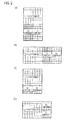
- FIG. 1 is a diagram that illustrates a positional relation between a block and a cell included in an image of an image processing device according to the present embodiment.
- the image processing device according to the present embodiment carries out processing in a unit of area (a block shown in FIG. 1(a) ) surrounded by 8-pixels in a scanning direction (that is horizontal direction) and 8-pixels in a vertical direction in an image which is composed of plural pixels arranged in a matrix state.
- Data of 1-pixel has 10-bits.
- the image processing device includes SDRAM (Synchronous Dynamic Random Access Memory).
- SDRAM Serial Dynamic Random Access Memory
- a word which is a unit in reading/writing (collectively called transfer) of SDRAM has 16-bits.
- an 8-words continuous transfer (burst access (burst transfer)) is carried out.
- the 12-pixels is called a cell for convenience.
- the cell corresponds to an area (12-pixels) surrounded by 3-pixels in the scanning direction and 4-pixels in the vertical direction, for example.
- data of 64-pixels is required.
- data of 8-pixels is not used to go to waste in image processing of a block of 8 ⁇ 8 pixels. This is because when 1-block and 6-cells are arranged in the scanning direction, both ends of them can not be aligned in the scanning direction.
- the image processing device carries out processing in a processing unit of 3-blocks.
- FIG. 1(d) when 3-blocks and 16-cells are arranged in the scanning direction of an image, both ends of them in the scanning direction are aligned.
- the number of blocks for the processing unit is increased, the volume of SRAM used in the image processing device needs to be increased. So, it is preferable that the number of blocks for the processing unit is 10 or less. It is noted that the block is not limited to the area surrounded by 8-pixels in the scanning direction and 8-pixels in the vertical direction.
- the block may be an area surrounded by 8-pixels in the scanning direction and 16-pixels in the vertical direction as shown in FIG. 2 (a) , or an area surrounded by 16-pixels in the scanning direction and 8-pixels in the vertical direction as shown in FIG. 2(b) .
- This block is composed of a luminance component (Y-component) area surrounded by 8-pixels in the scanning direction and 8-pixels in the vertical direction, a chrominance component (Cb-component) area surrounded by 4-pixels in the scanning direction and 8-pixels in the vertical direction, and a chrominance component (Cr-component) area surrounded by 4-pixels in the scanning direction and 8-pixels in the vertical direction, for example.
- This arrangement is called "4:2:2 chroma formal”.
- the block may be an area surrounded by 8-pixels in the scanning direction and 12-pixels in the vertical direction as shown in FIG. 2(c) , or an area surrounded by 12-pixels in the scanning direction and 8-pixels in the vertical direction as shown in FIG. 2(d) .
- This block is composed of a luminance component (Y-component) area surrounded by 8-pixels in the scanning direction and 8-pixels in the vertical direction, a chrominance component (Cb-component) area surrounded by 4-pixels in the scanning direction and 4-pixels in the vertical direction, and a chrominance component (Cr-component) area surrounded by 4-pixels in the scanning direction and 4-pixels in the vertical direction, for example.
- This arrangement is called "4:2:0 chroma format".
- the cell is also not be limited to 12-pixels.
- data of 1-pixel may have 12-bits and the cell has 10-pixels. If two SDRAMs are used to transfer 16-words (256-bits) twice larger than one SDRAM in one burst access, the number of pixels in the cell can be doubled.
- FIG. 3 is a block diagram that illustrates a configuration of the image processing device.
- the image processing device includes an image processor 1, SRAM 2, SDRAM 3, a data selector unit DS, a shift register unit 4, a data selector DS1, a counter 5, an SRAM address timing generator 6, an SRAM address generating table 7, an SDRAM signal generator 8 and an SDRAM parameter setting unit 9.
- SRAM 2 is a working memory. Since SRAM easily carries out a random access and realizes a medium-scale volume, SRAM is used as a working memory in the image processing device.
- a buffer for SDRAM 3 includes SRAM 2 (working memory) and the shift register unit 4 (arrangement of registers).
- SDRAM 3 has Banks (e.g., eight banks A to H), each of which has the same size, which are obtained by dividing a memory area into parts whose number is even.
- the SRAM address generating table 7 represents each relation between a pixel position in an image and an address in SDRAM 3 (Bank address, Row address and Column address). Namely, the SRAM address generating table 7 represents Bank address, Row address and Column address on SDRAM in which pixel data in each position is stored.
- the SDRAM parameter setting unit 9 is an element for setting and controlling an access amount and a cell shape of SDRAM 3.
- the SDRAM parameter setting unit 9 is provided because a different access control is required in an access for the same 3-blocks due to a difference in block shapes for luminance and chrominance or a difference in block shapes for "4:4:2 format" and "4:2:0 format".
- FIG. 4 is a diagram that illustrates a portion of the image processing device in detail.
- the data selector unit DS includes data selectors DS2, DS3 and DS4.
- the shift register unit 4 includes shift registers 4AB and 4CD.
- the data selector DS2 and the shift register 4AB are used to access to Banks A, C, E and G.
- the data selector DS3 and the shift register 4CD are used to access to Banks B, D, F and H.
- the shift register 4AB has a four stage shift register composed of registers 1a, 2a, 3a and 4a and a four stage shift register composed of registers 1b, 2b, 3b and 4b.
- the shift register 4CD has a four stage shift register composed of registers 1c, 2c, 3c and 4c and a four stage shift register composed of registers 1d, 2d, 3d and 4d.
- the data selectors DS2 and DS4 are connected to each other via 40-bits bus.
- the data selectors DS3 and DS4 are also connected to each other via 40-bits bus.
- Each of registers 1a, 2a, 3a, 4a, 1b, 2b, 3b and 4b and the data selector DS2 are connected to each other via 16-bits bus (total eight buses).
- Each of registers 1c, 2c, 3c, 4c, 1d, 2d, 3d and 4d and the data selector DS3 are also connected to each other via 16-bits bus (total eight buses).
- the registers 1a to 4a and the data selector DS1 are connected to each other via 16-bits bus, clock signal Ra-CLK and the like.
- the registers 1b to 4b and the data selector DS1 are connected to each other via 16-bits bus, clock signal Rb-CLK and the like.
- the registers 1c to 4c and the data selector DS1 are connected to each other via 16-bits bus, clock signal Rc-CLK and the like.
- the registers 1d to 4d and the data selector DS1 are connected to each other via 16-bits bus, clock signal Rd-CLK and the like.
- the data selector DS1 and SDRAM 3 are connected to each other via a signal DQS, a signal DQSN (signal generated by delaying signal DQS by half-clock cycle) and a 40-bits data signal DQ.
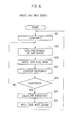
- FIG. 5 is a flowchart when data is read from SDRAM. It is here assumed that "the number of blocks necessary for aligning the right end of blocks with the right end of cells" in the explanation described with reference to FIG. 1 is three.
- the SRAM address timing generator 6 calculates addresses (Bank address, Row address and Column address) of three blocks in SDRAM not subject to processing, with reference to the SRAM address generating table 7 (S1).
- the SDRAM signal generator 8 controls SDRAM 3 according to an access timing of SDRAM 3.
- the SRAM address timing generator 6 carries out an access control of SRAM 2.
- the data selector DS1, the shift register unit 4 and the data selector unit DS carries out arrangement conversion and temporal retention of data of SRAM 2.
- the SDRAM signal generator 8 controls SDRAM 3 and carries out the arrangement conversion and the control of temporal retention.
- the SDRAM parameter setting unit 9 sets and controls an access amount and a cell shape of SDRAM 3.
- the counter 5 is initialized to have the value "0" (S5).
- the image processor 1 reads from SRAM 2 data of one block to be processed (S7).
- the SRAM address timing generator 6 generates an access control signal for reading.
- the image processor 1 processes the data of one block (S9).
- step S11 the value "1"' is added to the counter 5 (S11).
- step S13 it is determined whether or not the counter 5 has the value "3" (S13). If it is determined as NO, the processing returns to step S7. If it is determined as YES, the processing returns to step S1.
- FIG. 6 is a flowchart when data is written into SDRAM. It is also here assumed that "the number of blocks necessary for aligning the right end of blocks with the right end of cells" in the explanation described with reference to FIG. 1 is three.
- the counter 5 is initialized to have the value "0" (S21).
- the image processor 1 processes data of one block to be processed (S23).
- the image processor 1 writes the data into SRAM 2 (S25).
- the SRAM address timing generator 6 generates an access control signal for writing.
- step S27 the value "1" is added to the counter 5 (S27).
- step S29 it is determined whether or not the counter 5 has the value "3" (S29). If it is determined as NO, the processing returns to step S23.
- the SRAM address timing generator 6 calculates addresses (Bank address, Row address and Column address) of three blocks processed with reference to the SRAM address generating table 7 (S31).
- step S21 the data of three blocks processed is written to the calculated positions in SDRAM 3 from SRAM 2 via the data selector unit DS, the shift register unit 4 and the data selector DS1 (S33), and then the processing returns to step S21.
- the SDRAM signal generator 8 controls SDRAM 3 according to the access timing of SDRAM 3.
- the SRAM address timing generator 6 carries out the access control of SRAM 2.
- the data selector DS1, the shift register unit 4 and the data selector unit DS carries out the arrangement conversion and the temporal retention of data of SRAM 2.
- the SDRAM signal generator 8 controls SDRAM 3 and carries out the arrangement conversion and the control of temporal retention.
- the SDRAM parameter setting unit 9 sets and controls the access amount and the cell shape of SDRAM 3.
- the data selector unit DS, the shift register unit 4, the data selector DS1,the SDRAM signal generator 8 and the SDRAM parameter setting unit 9 of the image processing apparatus carry out parallel processing while causing the timing of one Bank access to differ from the timing of the other Bank access in two subsequent Bank accesses of SDRAM so as to reduce an idle time of SDRAM.
- FIG. 7 is a timing chart when data is read from Bank A and B of SDRAM.
- the data selector DS1 selects Bank A and reads from SDRAM 3 using the bus signal DQ of 16 bits, data to be transferred to the registers 1a to 4a and 1b to 4b.
- data transfer of 16 bits is carries out eight successive times.
- the data selector DS1 also transfers to the registers 1a to 4a as a clock signal Ra-CLK in a selection time of Bank A, a signal DQS output from SDRAM 3, and sends to the registers 1a to 4a via the bus signal of 16-bits, data for the registers 1a to 4a.
- the registers 1a to 4a obtain the data in the timing of the clock signal Ra-CLK.
- data transfer is carried out four successive times (four data transfers).
- the data selector DS 1 further transfers to the registers 1b to 4b as a clock signal Rb-CLK in the selection time of Bank A, a signal DQSN output from SDRAM, and sends to the registers 1b to 4b via the bus signal of 16-bits, data for the registers 1b to 4b.
- the registers 1b to 4b obtain the data in the timing of the clock signal Rb-CLK.
- data transfer is carried out four successive times (remaining four data transfers). Namely, four data transfers are carried out in the registers 1a to 4a while four data transfers which are delayed by a half clock are carried out in the registers 1b to 4b. Thus, total eight data transfers are carried out as one burst access.
- the data selector DS1 selects Bank B and reads from SDRAM 3 using the bus signal DQ of 16 bits, data to be transferred to the registers 1c to 4c and 1d to 4d.
- data transfer of 16 bits is carries out eight successive times.
- the data selector DS1 also transfers to the registers 1c to 4c as a clock signal Rc-CLK in a selection time of Bank B, a signal DQS output from SDRAM 3, and sends to the registers 1c to 4c via the bus signal of 16-bits, data for the registers 1c to 4c.
- the registers 1c to 4c obtain the data in the timing of the clock signal Rc-CLK.
- data transfer is carried out four successive times (four data transfers).
- the data selector DS1 further transfers to the registers 1d to 4d as a clock signal Rd-CLK in the selection time of Bank B, a signal DQSN output from SDRAM 3, and sends to the registers 1d to 4d via the bus signal of 16-bits, data for the registers 1d to 4d.
- the registers 1d to 4d obtain the data in the timing of the clock signal Rd-CLK.
- data transfer is carried out four successive times (remaining four data transfers).
- the data selectors DS2 and DS4 transfer data of the registers 1a to 4a and 1b to 4b to SRAM 2 via the bus signal of 40-bits.
- data transfer of 40-bits is carried out three times.
- Bank A is selected, and the data selectors DS3 and DS4 transfer to SRAM 2 via the bus signal of 40-bits, data of the registers 1c to 4c and 1d to 4d while the registers 1a to 4a and 1b to 4b obtain next data.
- SRAM-Ad represents an address signal of SRAM at the time of writing data into SRAM 2.
- SRAM-WEN represents a writing signal to SRAM at this time.
- the shift register unit 4 reads data of one of Banks A and B from SDRAM, it writes data of the other of Banks A and B into SRAM, and thereby the reading from SFRAM can be performed at high speed.
- the reading from Banks A, C, E and G and the reading from any one of Banks B, D, F and H can be performed at high speed.
- FIG. 8 is a timing chart when data is written into Bank A and B of SDRAM
- the data selectors DS2 and DS4 transfer to the registers 1a to 4a and 1b to 4b according to the timing of a signal Rab-Load, data to be sent from SRAM 2 via the bus signal of 40-bits.
- data transfer of 40-bits is carried out three times.
- the data selectors DS3 and DS4 transfer to the registers 1c to 4c and 1d to 4d according to the timing of a signal Rcd-Load, data to be sent from SRAM 2 via the bus signal of 40-bits.
- data transfer of 40-bits is carried out three times.
- SRAM-Ad represents an address signal of SRAM at the time of reading data from SRAM 2.
- SRAM-Data represents a data signal at this time.
- the data selector DS1 selects Bank A, transfers to SDRAM 3 as a device-to-SDRAM signal DQSw while the signal DQS is an SDRAM-to-device signal, a clock signal Raw-CLK (which is a device-to-SDRAM signal while the clock signal Ra-CLK is an SDRAM-to-device signal) output from the resisters 1a to 4a, and transfers data of the registers 1a to 4a to SDRAM 3 using the bus signal DQ of 16-bits.
- data transfer of 16-bits is carried out four times.
- the data selector DS1 transfers to SDRAM 3 as a device-to-SDRAM signal DQSNw while the signal DQSN is an SDRAM-to-device signal, a clock signal Rbw-CLK (which is a device-to-SDRAM signal while the clock signal Ra-CLK is an SDRAM-to-device signal) output from the resisters 1b to 4b, and transfers data of the registers 1b to 4b to SDRAM 3 using the bus signal DQ of 16-bits.
- data transfer of 16-bits is carried out four times. Namely, four data transfers are carried out in the registers 1a to 4a while four data transfers which are delayed by a half clock are carried out in the registers 1b to 4b. Thus, total eight data transfers are carried out as one burst access.
- the data selector DS1 selects Bank B and transfers data of the registers 1c to 4c and 1d to 4d to SDRAM 3 via the bus signals of 16-bits.
- data transfer of 16-bits is carried out eight times.
- the shift register unit 4 reads data of one of Banks A and B from SDRAM, it writes data of the other of Banks A and B into SRAM, and thereby the reading from SDRAM can be performed at high speed.
- the reading from Banks A, C, E and G and the reading from any one of Banks B, D, F and H can be performed at high speed.
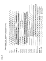
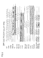
- FIG. 9 is a diagram that illustrates a relation between data of 16-bits and data of 40-bits to be read from or written into SDRAM 3. In reading from SDRAM 3, a data conversion having the following relation is carried out.
- the data selector DS1 reads 16-bits word from SDRAM 3 eight times, and causes the shift register 4AB to hold them, for example. Namely, the data selector DS1 reads 128-bits composed of words Wa0 to Wa7, and causes the shift register 4AB to hold them, for example.
- the data selector unit DS writes into SRAM 2, data having four 10-bits words held in the shift register 4AB three times, for example. Namely, the data selector unit DS converts the words Wa0 to Wa7 into 120-bits composed of words W00 to W03, W10 to W13, W20 to W23 and W30 to W33, and writes them into SRAM 2. Remained 8-bits are removed in the shift register 4AB and the data selector unit DS, for example.
- the image processor 1 reads the words W00 to W03, W10 to W13 and W20 to W23 from SRAM 2.
- the image processor 1 writes into SRAM 2, 120-bits composed of words W00 to W03, W10 to W13 and W20 to W23.
- the data selector unit DS reads from SRAM 2, the words W00 to W03, W10 to W13 and W20 to W23, and causes the shift register 4AB to hold them, for example. Remained 8-bits are added to the words W00 to W03, W10 to W13 and W20 to W23.
- the data selector DS1 converts into words Wa1 to Wa8 the 128-bits to which the 8-bits are added, and writes them into SDRAM3.
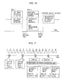
- a first command Cmd-1 an address of Bank of an access target and a desired Row address in Bank of the access target are set in Active.
- a second command Cmd-2 the address of Bank of the access target, a start address of Column on the desired Row address in Bank of the access target, and Read/Write mode (including a bust access setting) are designated after a predetermined time (Cmd-2 waiting time) has elapsed from the time when the first command Cmd-1 is issued.
- a predetermined time burst delay time
- Read or Write operation is carried out by a burst access (8-words continuous transfer) from the designated start address of Column as a stating point.
- the data of 32 words is divided into four segments each having 8-words and the four segments are respectively arranged in four Bank A, B, C and D because it is impossible to carry out a continuous burst access to different Row addresses of the same Bank in SDRAM.
- first commands Cmd-1A, Cmd-1B, Cmd-1C and Cmd-1D are initially issued and then addresses of Banks A, B, C and D of access targets and desired Row addresses in Bank A, B, C and D of the access targets are set in Active (not shown in FIG. 11 ).
- second commands Cmd-2A, Cmd-2B, Cmd-2C and Cmd-2D are issued and then the addresses of Banks A, B, C and D of the access targets, start addresses (X1, Y1 and the like) of Columns on the desired Row addresses in Banks A, B, C and D of the access targets, and Read modes are designated.
- duration of each command duration of burst delay time and duration of 8-words burst access are respectively one clock, six clocks and four clocks, if the second command is issued in every four clocks, the burst access is effectively and continuously carried out (see FIG. 11 ).
- the Cmd-2 waiting time and the burst delay time are previously determined as specification of SDRAM.
- the Cmd-2 waiting time coincides with a period until three first commands have been issued
- the second command Cmd-2A is issued after the first commands Cmd-1A, Cmd-1B and Cmd-1C have been issued, so as to effectively and continuously carry out the burst access.
- the second commands Cmd-2B, Cmd-2C and Cmd-2D are issued.
- a delay from the issue of first command until the start of its burst access requires about 12 clocks.
- the first commands firstly issued can be commonly used.
- a delay from the issue of second command until the start of its burst access requires about eight clocks.
- the first command can be issued in every eight clock circles or less.
- the maximum access amount per unit time is realized. Also, by carrying out similar processing at the time of Write operation, the maximum access amount per unit time is realized.
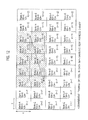
- FIG. 12 is a diagram that illustrates a formation example of image data in one frame in the case where the amount of burst access is 128-bits when one word of SDRAM has 16-bits and image data has 10-bits/pixel.
- a cell has 3-pixels in a horizontal direction and 4-pixels in a vertical direction. It is desirable to include descriptions of Bank address, Row address and Column address in the cell.
- the third row ⁇ cells are repeatedly arranged in order of Banks A, B, C and D and Column addresses are changed. If Column address reaches the maximum value, Row addresses are changed and cells are repeatedly arranged in order of Banks A, B, C and D.
- the four row ⁇ cells are repeatedly arranged in order of Banks E, F, G and H and Column addresses are changed. If Column address reaches the maximum value, Row addresses are changed and cells are repeatedly arranged in order of Banks E, F, G and H and Column addresses are changed. If Column address reaches the maximum value, Row addresses are changed and cells are repeatedly arranged in order of Banks E, F, G and H.
- FIG. 12 an access along a line arrow in a hatching rectangular region of 5x2 will be described.
- a continuous access can not be carried out.
- a continuous burst access can be carried out because the arrangement of Banks in an upper row differs from that in a lower row.
- a reason why eight Banks are alternately arranged is as follows. If an alternate burst access to two or more Banks is not carried out, the maximum access speed can not be obtained. That is, since a gap occurs between bursts in a continuous access to the same Bank, the maximum access speed is not continuously realized.
- FIG. 13 is a timing chart when the image data structure of FIG. 12 is employed.
- FIG. 13 illustrates operations of eight Banks and two pairs of register groups in Read operation or Write operation along the line arrow in the rectangular region of 5 ⁇ 2 cells in FIG. 12 .
- SRAM access the data transfer operation between SDRAM access buffer registers (sorting registers) and input-and-output of the image processing device are carried out.
- Read operation corresponds to SRAM access after SDRAM access, and the read Bank data is transferred to SRAM of the image processing device.
- Write operation of SDRAM it corresponds to SDRAM access after SRAM access, and data from the image processing device to be written subsequently is transferred from SRAM of the image processing device to the SDRAM access buffer register.
- one burst access only need to have 12-pixels (e.g., 6-pixels ⁇ 2-lines).
- a method of using all 12-pixels as luminance pixels or chrominance pixels is possible for 4:2:2 chroma format.
- different Banks may be used for a luminance signal and a chrominance signal
- different Row addresses may be set for a luminance and a chrominance.
- 12-pixels may be divided into 6-pixels for a luminance and 6-pixels for a chrominance.
- one pixel is processed with 10-bits. If one pixel is processed with 12-bits, for correspondence between a data width of 12-bits and a SDRAM high speed burst access unit of 128-bits, it is assumed that ten data widths of 12-bits are included in 128-bits.
- an arrangement in an image memory has 1 ⁇ 10, 2 ⁇ 5, 5x2 or 10 ⁇ 1, and an optimal arrangement is selected from them.
- a burst access unit When SDRAMs with two chips configuration are used in parallel, a burst access unit has 256-bits. At this time, there are a manner in which 256-bits is represented by 12-bits ⁇ 21+4-bits and a manner in which 256-bits is represented by 12-bits ⁇ 20+16-bits. If 21-pixels is used, an arrangement in an image memory has 1 ⁇ 21, 3 ⁇ 7, 7 ⁇ 3 or 21 ⁇ 1. If 20-pixels is used, an arrangement in an image memory has 1x20, 2 ⁇ 10, 4 ⁇ 5, 5 ⁇ 4, 10 ⁇ 2 or 20 ⁇ 1.
- the present embodiment can be applied.
- FIG. 14 illustrates that a continuous burst access with efficiency is also realized by a zigzag access in place of an access to an adjacent region in a horizontal direction or a continuous access to an upper limit adjacent region in a vertical direction.
- SDRAM is essential for implementation of an encoder or a decoder for motion picture. Recently, SDRAM is developed in order of DDR, DDR2 and DDR3. A storage capacity of current mainstream DDR3 SDRAM has about 1-Gbits to 2Gbits. This capacity can store hi-vision images by 30 to 60 frames. Since the encoder or decoder of H.264 is normally realized with a storage capacity having about 4 to 6 frames, recent SDRAM has enough capacity as a storage requirement.
- an invention to increase access efficiency is required in view of SDRAM.
- an operation speed of SDRAM has a clock frequency of 500MHz or more and image signal processing is carried out in parallel.
- the present invention realizes an encoder and a decoder suitable for such situation, and produces an effect for various image signal processing applications (a medical image, a frame frequency conversion, an image recognizing device and the like).
- HDD Hard Disk Drive
- HDD has a configuration of a conventional power-of-two value unit, and an access speed for storage capacity of HDD recently increases.
- AV Audiovisual
- DVD Digital Versatile Disk
- BD Blue-ray Disk
- the effect of the present invention is applied to realization of a high quality signal processing device.
- a sector size (about 2048-bites) of a digital storage medium such as HDD, DVD or BD is larger than the burst size of SDRAM described above.
- a data configuration of 8-bits unit (bite) may be converted into a data configuration of 10-bits unit or 12-bits unit, for every 128-bits (16-bites) or 256-bits (32-bites).
Landscapes
- Engineering & Computer Science (AREA)
- Theoretical Computer Science (AREA)
- Physics & Mathematics (AREA)
- General Physics & Mathematics (AREA)
- Human Computer Interaction (AREA)
- General Engineering & Computer Science (AREA)
- Dram (AREA)
- Image Input (AREA)
- Image Processing (AREA)
Applications Claiming Priority (2)
| Application Number | Priority Date | Filing Date | Title |
|---|---|---|---|
| JP2010138566 | 2010-06-17 | ||
| PCT/JP2011/063067 WO2011158699A1 (fr) | 2010-06-17 | 2011-06-07 | Dispositif de traitement d'image |
Publications (2)
| Publication Number | Publication Date |
|---|---|
| EP2584524A1 true EP2584524A1 (fr) | 2013-04-24 |
| EP2584524A4 EP2584524A4 (fr) | 2017-05-24 |
Family
ID=45348104
Family Applications (1)
| Application Number | Title | Priority Date | Filing Date |
|---|---|---|---|
| EP11795607.8A Withdrawn EP2584524A4 (fr) | 2010-06-17 | 2011-06-07 | Dispositif de traitement d'image |
Country Status (6)
| Country | Link |
|---|---|
| US (1) | US9286018B2 (fr) |
| EP (1) | EP2584524A4 (fr) |
| JP (1) | JP5616965B2 (fr) |
| CN (1) | CN102947859B (fr) |
| CA (1) | CA2802666C (fr) |
| WO (1) | WO2011158699A1 (fr) |
Families Citing this family (2)
| Publication number | Priority date | Publication date | Assignee | Title |
|---|---|---|---|---|
| US9430992B2 (en) * | 2011-03-10 | 2016-08-30 | Ntt Electronics Corporation | Memory access device |
| US9514510B2 (en) * | 2013-03-29 | 2016-12-06 | Mediatek Inc. | Method and apparatus for arranging pixels of picture in storage units each having storage size not divisible by pixel size |
Family Cites Families (12)
| Publication number | Priority date | Publication date | Assignee | Title |
|---|---|---|---|---|
| JPS5881383A (ja) * | 1981-11-11 | 1983-05-16 | Dainippon Screen Mfg Co Ltd | 2値画像のデ−タ圧縮方法 |
| JPH10269706A (ja) * | 1997-03-27 | 1998-10-09 | Sony Corp | 情報再生装置及び情報再生方法 |
| JP3687269B2 (ja) * | 1997-05-08 | 2005-08-24 | ブラザー工業株式会社 | 画像処理装置 |
| US6456746B2 (en) * | 1999-01-26 | 2002-09-24 | Sarnoff Corporation | Method of memory utilization in a predictive video decoder |
| JP2001144716A (ja) | 1999-11-12 | 2001-05-25 | Matsushita Electric Ind Co Ltd | 映像信号の時分割多重分離装置 |
| US6801209B1 (en) * | 1999-12-30 | 2004-10-05 | Intel Corporation | Method and apparatus for storing data in a block-based memory arrangement |
| JP2004264540A (ja) * | 2003-02-28 | 2004-09-24 | Toshiba Tec Corp | 画像形成装置及び画像形成装置の画像表示方法 |
| JP2004334295A (ja) * | 2003-04-30 | 2004-11-25 | Yamaha Corp | 記憶装置 |
| JP4909779B2 (ja) * | 2006-04-17 | 2012-04-04 | パナソニック株式会社 | 画像データ転送方法、画像処理装置、及び撮像システム |
| US20090070570A1 (en) * | 2007-09-11 | 2009-03-12 | Shubhodeep Roy Choudhury | System and Method for Efficiently Handling Interrupts |
| JP2009116763A (ja) * | 2007-11-09 | 2009-05-28 | Sony Corp | 画像処理装置および画像データのメモリアクセス方法 |
| WO2010014696A1 (fr) * | 2008-07-29 | 2010-02-04 | Marvell World Trade, Ltd. | Traitement de données rastérisées |
-
2011
- 2011-06-07 US US13/704,303 patent/US9286018B2/en not_active Expired - Fee Related
- 2011-06-07 CN CN201180029707.XA patent/CN102947859B/zh not_active Expired - Fee Related
- 2011-06-07 JP JP2012520382A patent/JP5616965B2/ja not_active Expired - Fee Related
- 2011-06-07 EP EP11795607.8A patent/EP2584524A4/fr not_active Withdrawn
- 2011-06-07 CA CA2802666A patent/CA2802666C/fr active Active
- 2011-06-07 WO PCT/JP2011/063067 patent/WO2011158699A1/fr not_active Ceased
Non-Patent Citations (1)
| Title |
|---|
| See references of WO2011158699A1 * |
Also Published As
| Publication number | Publication date |
|---|---|
| EP2584524A4 (fr) | 2017-05-24 |
| CN102947859B (zh) | 2016-03-30 |
| CA2802666A1 (fr) | 2011-12-22 |
| WO2011158699A1 (fr) | 2011-12-22 |
| CN102947859A (zh) | 2013-02-27 |
| US20130088756A1 (en) | 2013-04-11 |
| JPWO2011158699A1 (ja) | 2013-08-19 |
| JP5616965B2 (ja) | 2014-10-29 |
| US9286018B2 (en) | 2016-03-15 |
| CA2802666C (fr) | 2015-08-11 |
Similar Documents
| Publication | Publication Date | Title |
|---|---|---|
| JP5126360B2 (ja) | メモリ装置及びそれを制御するメモリコントローラ | |
| US8918589B2 (en) | Memory controller, memory system, semiconductor integrated circuit, and memory control method | |
| CN101495975A (zh) | 存储控制装置、存储装置及存储控制方法 | |
| CN106201363B (zh) | 视频流像素级数据随机实时访问的存储器及存储方法 | |
| CN103237157B (zh) | 一种实时高清视频图像转置器 | |
| CN100446084C (zh) | 画面数据传送方法、影像数据传送方法以及时序控制模块 | |
| US7061496B2 (en) | Image data processing system and image data reading and writing method | |
| CN102625086B (zh) | 一种用于高清数字矩阵的ddr2存储方法和系统 | |
| US9286018B2 (en) | Image processing device for improved access efficiency | |
| JP6131357B1 (ja) | 半導体記憶装置とそのアドレス制御方法 | |
| JP2003007052A (ja) | 半導体記憶装置およびそれを用いたメモリシステム | |
| JP2007122706A (ja) | メモリマッピング方法及び装置 | |
| CN101903868B (zh) | 存储装置以及其控制方法 | |
| Gong et al. | Design of high-speed real-time sensor image processing based on FPGA and DDR3 | |
| KR101068829B1 (ko) | 촬상 장치 및 이미지 회전 처리 방법 | |
| JPH0564091A (ja) | ビデオカメラ | |
| JPH09106669A (ja) | シンクロナスdramと半導体記憶装置 | |
| US7366823B2 (en) | Method and system for memory access | |
| JP2020030521A (ja) | 画像処理装置 | |
| CN103813072A (zh) | 信号处理电路、成像装置及程序 | |
| JP2012113597A (ja) | メモリ装置、メモリ制御回路及びメモリ制御システム | |
| JP2008146235A (ja) | 画像処理装置 | |
| JP4415785B2 (ja) | 画像信号処理装置およびその方法 | |
| JP2000284771A (ja) | 映像データ処理装置 | |
| JP2007279902A (ja) | メモリ制御方法、メモリ制御装置、画像処理装置およびプログラム |
Legal Events
| Date | Code | Title | Description |
|---|---|---|---|
| PUAI | Public reference made under article 153(3) epc to a published international application that has entered the european phase |
Free format text: ORIGINAL CODE: 0009012 |
|
| 17P | Request for examination filed |
Effective date: 20130110 |
|
| AK | Designated contracting states |
Kind code of ref document: A1 Designated state(s): AL AT BE BG CH CY CZ DE DK EE ES FI FR GB GR HR HU IE IS IT LI LT LU LV MC MK MT NL NO PL PT RO RS SE SI SK SM TR |
|
| DAX | Request for extension of the european patent (deleted) | ||
| RA4 | Supplementary search report drawn up and despatched (corrected) |
Effective date: 20170426 |
|
| RIC1 | Information provided on ipc code assigned before grant |
Ipc: G06T 1/60 20060101AFI20170420BHEP |
|
| STAA | Information on the status of an ep patent application or granted ep patent |
Free format text: STATUS: EXAMINATION IS IN PROGRESS |
|
| 17Q | First examination report despatched |
Effective date: 20190205 |
|
| GRAP | Despatch of communication of intention to grant a patent |
Free format text: ORIGINAL CODE: EPIDOSNIGR1 |
|
| STAA | Information on the status of an ep patent application or granted ep patent |
Free format text: STATUS: GRANT OF PATENT IS INTENDED |
|
| RIC1 | Information provided on ipc code assigned before grant |
Ipc: G06T 3/40 20060101ALI20201006BHEP Ipc: G06T 1/60 20060101AFI20201006BHEP |
|
| INTG | Intention to grant announced |
Effective date: 20201028 |
|
| STAA | Information on the status of an ep patent application or granted ep patent |
Free format text: STATUS: THE APPLICATION IS DEEMED TO BE WITHDRAWN |
|
| 18D | Application deemed to be withdrawn |
Effective date: 20210310 |