EP2584647A2 - Dispositif de communication et structure d'antenne associée - Google Patents
Dispositif de communication et structure d'antenne associée Download PDFInfo
- Publication number
- EP2584647A2 EP2584647A2 EP12160075.3A EP12160075A EP2584647A2 EP 2584647 A2 EP2584647 A2 EP 2584647A2 EP 12160075 A EP12160075 A EP 12160075A EP 2584647 A2 EP2584647 A2 EP 2584647A2
- Authority
- EP
- European Patent Office
- Prior art keywords
- communication device
- ground element
- open slot
- substrate
- metal portion
- Prior art date
- Legal status (The legal status is an assumption and is not a legal conclusion. Google has not performed a legal analysis and makes no representation as to the accuracy of the status listed.)
- Withdrawn
Links
- 238000004891 communication Methods 0.000 title claims abstract description 54
- 239000002184 metal Substances 0.000 claims abstract description 52
- 239000000758 substrate Substances 0.000 claims abstract description 34
- 239000004020 conductor Substances 0.000 claims description 17
- 230000005404 monopole Effects 0.000 claims description 7
- 238000010586 diagram Methods 0.000 description 12
- 230000008878 coupling Effects 0.000 description 4
- 238000010168 coupling process Methods 0.000 description 4
- 238000005859 coupling reaction Methods 0.000 description 4
- 238000004088 simulation Methods 0.000 description 4
- 238000013461 design Methods 0.000 description 3
- 230000005540 biological transmission Effects 0.000 description 1
- 230000001419 dependent effect Effects 0.000 description 1
- 238000011161 development Methods 0.000 description 1
- 230000018109 developmental process Effects 0.000 description 1
- 238000005516 engineering process Methods 0.000 description 1
- 238000005259 measurement Methods 0.000 description 1
- 238000000034 method Methods 0.000 description 1
- 238000010295 mobile communication Methods 0.000 description 1
Images


Classifications
-
- H—ELECTRICITY
- H01—ELECTRIC ELEMENTS
- H01Q—ANTENNAS, i.e. RADIO AERIALS
- H01Q1/00—Details of, or arrangements associated with, antennas
- H01Q1/36—Structural form of radiating elements, e.g. cone, spiral, umbrella; Particular materials used therewith
- H01Q1/38—Structural form of radiating elements, e.g. cone, spiral, umbrella; Particular materials used therewith formed by a conductive layer on an insulating support
-
- H—ELECTRICITY
- H01—ELECTRIC ELEMENTS
- H01Q—ANTENNAS, i.e. RADIO AERIALS
- H01Q1/00—Details of, or arrangements associated with, antennas
- H01Q1/12—Supports; Mounting means
- H01Q1/22—Supports; Mounting means by structural association with other equipment or articles
- H01Q1/24—Supports; Mounting means by structural association with other equipment or articles with receiving set
- H01Q1/241—Supports; Mounting means by structural association with other equipment or articles with receiving set used in mobile communications, e.g. GSM
- H01Q1/242—Supports; Mounting means by structural association with other equipment or articles with receiving set used in mobile communications, e.g. GSM specially adapted for hand-held use
- H01Q1/243—Supports; Mounting means by structural association with other equipment or articles with receiving set used in mobile communications, e.g. GSM specially adapted for hand-held use with built-in antennas
-
- H—ELECTRICITY
- H01—ELECTRIC ELEMENTS
- H01Q—ANTENNAS, i.e. RADIO AERIALS
- H01Q13/00—Waveguide horns or mouths; Slot antennas; Leaky-waveguide antennas; Equivalent structures causing radiation along the transmission path of a guided wave
- H01Q13/10—Resonant slot antennas
-
- H—ELECTRICITY
- H01—ELECTRIC ELEMENTS
- H01Q—ANTENNAS, i.e. RADIO AERIALS
- H01Q5/00—Arrangements for simultaneous operation of antennas on two or more different wavebands, e.g. dual-band or multi-band arrangements
- H01Q5/40—Imbricated or interleaved structures; Combined or electromagnetically coupled arrangements, e.g. comprising two or more non-connected fed radiating elements
-
- H—ELECTRICITY
- H01—ELECTRIC ELEMENTS
- H01Q—ANTENNAS, i.e. RADIO AERIALS
- H01Q9/00—Electrically-short antennas having dimensions not more than twice the operating wavelength and consisting of conductive active radiating elements
- H01Q9/04—Resonant antennas
- H01Q9/30—Resonant antennas with feed to end of elongated active element, e.g. unipole
- H01Q9/42—Resonant antennas with feed to end of elongated active element, e.g. unipole with folded element, the folded parts being spaced apart a small fraction of the operating wavelength
Definitions
- This invention relates to a communication device having a monopole slot antenna and a monopole strip antenna integrated therein, where the operating bandwidth of the communication device covers at least the 824-960 MHz and 1710-2170 MHz bands, according to the pre-characterizing clause of Claim 1.
- a mobile device With the advance of mobile technology, a mobile device needs to be lighter in weight and more compact in appearance. Meanwhile, the ever-evolving communication specification requires wider operating bandwidth as well.
- a clearance space is generally disposed on the top or at the bottom of a communication device, such that the overall Q value (Quality factor) of the antenna drops and the operating bandwidth is increased to cover multiband operations.
- Q value Quality factor
- U.S. Patent No. 7,932,865 B2 entitled "Coplanar coupled-fed multiband antenna for the mobile device” discloses a multi band built-in antenna design. However, this method cannot utilize the clearance region to further increase operating bandwidth to cover more operating frequency bands.
- a communication device having two wideband operating bands that, for example, cover at least about 824-960 MHz and 1710-2170 MHz bands for the penta-band WWAN (wireless wide area network) operation, and in addition, the antenna therein closely integrates with nearby electronic elements in the communication device.
- WWAN wireless wide area network
- the invention aims at providing a communication device that can cover the penta-band WWAN operation and closely integrate with nearby electronic elements therein. This is achieved by a communication device having a monopole slot antenna and a monopole strip antenna integrated therein according to Claim 1.
- the dependent claims pertain to corresponding further developments and improvements.
- a claimed exemplary communication device including a substrate, a ground element, an open slot and a radiating metal portion.
- the ground element is disposed on a first surface of the substrate.
- the open slot is formed on the ground element and substantially parallel with an edge of the ground element, wherein the open slot at least generates a first resonant mode, and a distance between the open slot and the edge of the ground element is shorter than 0.05 wavelength of a center frequency of the first resonant mode.
- the radiating metal portion is disposed on a second surface of the substrate, wherein the open slot at least partially covers the radiating metal portion, the radiating metal portion at least generates a second resonant mode, and a feed point of the radiating metal portion is electrically coupled to a signal source on the substrate.
- a claimed antenna structure including a substrate, a ground element, an open slot and a radiating metal portion.
- the ground element is disposed on a first surface of the substrate.
- the open slot is formed on the ground element and substantially parallel with an edge of the ground element, wherein the open slot at least generates a first resonant mode, and a distance between the open slot and the edge of the ground element is shorter than 0.05 wavelength of a center frequency of the first resonant mode.
- the radiating metal portion is disposed on a second surface of the substrate, wherein the open slot at least partially covers the radiating metal portion, the radiating metal portion at least generates a second resonant mode, and a feed point of the radiating metal portion is electrically coupled to a signal source on the substrate.
- the open slot is substantially rectangle-shaped, and generates the first resonant mode in the first operating band of the communication device.
- the open slot since the open slot at least partially covers the radiating metal portion, the open slot may be used as a clearance region for the radiating metal portion, such that the radiating metal portion may be a monopole strip antenna, generating the second resonant mode in the second operating band of the communication device.
- the radiating metal portion may also be used as the feed structure of the open slot to effectively excite the open slot.
- the generated first operating band may cover at least about 824-960 MHz band
- the second operating band may cover at least about 1710-2170 MHz band, such that the communication device may cover the penta-band WWAN operation.
- the edge of the ground element may also be electrically coupled to a metal conductor.
- the metal conductor has a width, and is substantially perpendicular to the ground element.
- the width of the metal conductor is not larger than the thickness of the communication device.
- the metal conductor may excite the ground element, which increases the bandwidth of the first resonant mode, covers more operating bands, and may be part of the housing of the communication device.
- the metal conductor integrates with an electronic element, and part of the electronic element is electrically coupled to the ground element.
- FIG. 1 is a schematic diagram illustrating a communication device 1 and its antenna structure according to a first embodiment of the present invention.
- the communication device 1 includes a ground element 11, a substrate 12, an open slot 13 and a radiating metal portion 14.
- the ground element 11 is disposed on a first surface 121 of the substrate 12.
- the open slot 13 is formed on the ground element 11, and the open slot 13 is substantially parallel with an edge 111 of the ground element 11.
- the open slot 13 generates at least a first resonant mode, and a distance d between the open slot 13 and the edge 111 of the ground element 11 is shorter than 0.05 wavelength ( ⁇ ) of a center frequency of the first resonant mode (i.e., d ⁇ 0.05 ⁇ ), such that the open slot 13 is sufficiently close to the edge 111 of the ground element 11 to therefore have practical application value.
- the radiating metal portion 14 is disposed on a second surface 122 of the substrate 12, and the open slot 13 at least partially covers the radiating metal portion 14.
- the radiating metal portion 14 at least generates a second resonant mode and increases operating bandwidth of the communication device 1.
- a feed point 141 of the radiating metal portion 14 is electrically coupled to a signal source 15 disposed on the substrate 12.
- the open slot 13 is substantially rectangular, but this is not meant to be a limitation of the present invention.
- the radiating metal portion 14 may be a monopole strip antenna, but the present invention is not limited to this.
- FIG. 2 is a schematic diagram illustrating a communication device 2 and its antenna structure according to a second embodiment of the present invention
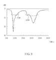
- FIG. 3 is a schematic diagram illustrating the return loss of the communication device 2 and its antenna structure.
- the communication device 2 and its antenna structure in FIG. 2 further includes a metal conductor 26, and the edge 111 of the ground element 11 is electrically coupled to the metal conductor 26 via a coupling point 271 and a coupling point 272.
- the metal conductor 26 is substantially perpendicular to the ground element 11, and has a width not larger than a thickness of the communication device 2.
- the metal conductor 26 may be a part of a housing of the communication device 2, but this is not meant to be a limitation of the present invention. Due to the fact that the antenna structure of the communication device 2 in the second embodiment is similar to the antenna structure of the communication device 1 in the first embodiment, the second embodiment may also have functions similar to that of the first embodiment.
- the length of the substrate 12 is about 110 mm, the width of the substrate 12 is about 60 mm, and the thickness of the substrate 12 is about 0.8 mm; the ground element 11 is formed on the substrate 12; the length of the open slot 13 is about 40 mm, and the width of the open slot 13 is about 9 mm. Due to the open slot 13 being printed on the substrate 12 which is a dielectric substrate, the length of the open slot 13 is about 0.12 wavelength of the center frequency (about 890 MHz) of first operating band 2100, and thus the length of the open slot 13 is shorter than a quarter wavelength of the center frequency. As shown in FIG.
- the second embodiment of the present invention operates under the 6-dB return loss (widely used design specification for a mobile communication device antenna), the first operating band 2100 may cover about 824-960 MHz for the GSM850/900 operation, the second operating band 2200 may cover about 1710-2170 MHz for the GSM1800/1900/UMTS operation, and thus the antenna structure may cover the penta-band WWAN operation.
- FIG. 4 is a schematic diagram illustrating a communication device 3 and its conventional antenna structure according to the prior art
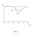
- FIG. 5 is a schematic diagram illustrating a simulation of return loss of communication device 3 and its conventional antenna structure.
- the communication device 3 includes a ground element 31, a substrate 32, and a radiating metal portion 34.
- the ground element 31 is disposed on a first surface 321 of the substrate 32.
- the radiating metal portion 34 is disposed in a clearance region 3211 on the substrate 32, and a feed point 341 of the radiating metal portion 34 is electrically coupled to a signal source 35 disposed on the substrate 32.
- the difference between the communication device 3 and its conventional antenna structure and the communication device 1 and its antenna structure in the first embodiment of the present invention is that the communication device 3 and its conventional antenna structure only generate the resonant mode from the radiating metal portion 34, and fail to exploit the clearance region 3211 to form the open slot so as to increase the operating bandwidth.
- the length of the substrate 32 is about 110 mm, the width of the substrate 32 is about 60 mm, the thickness of the substrate 32 is about 0.8 mm; the ground element 31 is formed on the substrate 32; and the length of the radiating metal portion 34 is about 34 mm.
- the communication device 3 and its conventional antenna structure operate under 6-dB return-loss definition, the operating band 3100 thereof may only cover the GSM1800/1900/UMTS operation, when compared to the second embodiment of the present invention as shown in FIG. 3 .
- the conventional antenna structure fails to generate a resonant mode in the desired low-frequency band, and is therefore unable to cover the penta-band WWAN operation.
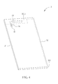
- FIG. 6 is a structure diagram illustrating a communication device 4 and its antenna structure according to a third embodiment of the present invention.
- the main difference between the antenna structure of the third embodiment and the antenna structure of the first embodiment is that the edge 111 of the ground element 11 of the communication device 4 and its antenna structure in FIG. 6 is electrically coupled to a metal conductor 46 via a coupling point 471 and a coupling point 472.
- the metal conductor 46 is substantially perpendicular to the ground element 11.
- the width of the metal conductor 46 is shorter than the thickness of the communication device 4.
- the metal conductor 46 can integrate with an electronic element 48 such as a data transmission adapter or a USB (universal serial bus) connector, and part of the structure of the electronic element 48 is electrically coupled to the ground element 11. Due to the fact that the antenna structure of the third embodiment is similar to the antenna structure of the first embodiment, the third embodiment may also have functions similar to that of the first embodiment.
- an electronic element 48 such as a data transmission adapter or a USB (universal serial bus) connector
Landscapes
- Physics & Mathematics (AREA)
- Electromagnetism (AREA)
- Engineering & Computer Science (AREA)
- Computer Networks & Wireless Communication (AREA)
- Details Of Aerials (AREA)
- Support Of Aerials (AREA)
- Waveguide Aerials (AREA)
Applications Claiming Priority (1)
| Application Number | Priority Date | Filing Date | Title |
|---|---|---|---|
| TW100138154A TWI483464B (zh) | 2011-10-20 | 2011-10-20 | 通訊裝置及其天線結構 |
Publications (2)
| Publication Number | Publication Date |
|---|---|
| EP2584647A2 true EP2584647A2 (fr) | 2013-04-24 |
| EP2584647A3 EP2584647A3 (fr) | 2013-10-09 |
Family
ID=45999561
Family Applications (1)
| Application Number | Title | Priority Date | Filing Date |
|---|---|---|---|
| EP12160075.3A Withdrawn EP2584647A3 (fr) | 2011-10-20 | 2012-03-19 | Dispositif de communication et structure d'antenne associée |
Country Status (3)
| Country | Link |
|---|---|
| US (1) | US9325059B2 (fr) |
| EP (1) | EP2584647A3 (fr) |
| TW (1) | TWI483464B (fr) |
Cited By (10)
| Publication number | Priority date | Publication date | Assignee | Title |
|---|---|---|---|---|
| EP2629368A1 (fr) * | 2012-02-14 | 2013-08-21 | HTC Corporation | Dispositif mobile |
| EP2650963A1 (fr) * | 2012-04-09 | 2013-10-16 | HTC Corporation | Dispositif mobile et son procédé de fabrication |
| CN104538741A (zh) * | 2014-12-17 | 2015-04-22 | 小米科技有限责任公司 | 缝隙天线及具有导电边框的电子设备 |
| WO2015124463A1 (fr) * | 2014-02-18 | 2015-08-27 | Antennentechnik Bad Blankenburg Gmbh | Antenne à plusieurs gammes de fréquences pour un dispositif émetteur et/ou récepteur destiné à une utilisation mobile |
| US9331379B2 (en) | 2012-02-14 | 2016-05-03 | Htc Corporation | Mobile device and manufacturing method thereof |
| CN107658556A (zh) * | 2017-09-04 | 2018-02-02 | 深圳市盛路物联通讯技术有限公司 | 无线通信设备 |
| CN108604731A (zh) * | 2016-01-28 | 2018-09-28 | 索尼移动通讯有限公司 | 电路板上的天线结构 |
| CN109286077A (zh) * | 2017-07-19 | 2019-01-29 | 启碁科技股份有限公司 | 移动装置 |
| CN109904598A (zh) * | 2017-12-08 | 2019-06-18 | 财团法人工业技术研究院 | 多频多天线阵列 |
| CN115224482A (zh) * | 2021-04-16 | 2022-10-21 | 台达电子工业股份有限公司 | 天线结构以及无线通信装置 |
Families Citing this family (4)
| Publication number | Priority date | Publication date | Assignee | Title |
|---|---|---|---|---|
| TWI643404B (zh) * | 2016-02-18 | 2018-12-01 | 達意科技股份有限公司 | 槽孔天線裝置 |
| TWI621305B (zh) * | 2016-06-28 | 2018-04-11 | 國立高雄師範大學 | 開槽孔天線 |
| TWI653786B (zh) * | 2017-07-25 | 2019-03-11 | 和碩聯合科技股份有限公司 | 電子裝置 |
| US10644407B2 (en) * | 2018-01-14 | 2020-05-05 | Wistron Neweb Corp. | Communication device |
Citations (1)
| Publication number | Priority date | Publication date | Assignee | Title |
|---|---|---|---|---|
| US7932865B2 (en) | 2008-05-05 | 2011-04-26 | Acer Incorporated | Coplanar coupled-fed multiband antenna for the mobile device |
Family Cites Families (7)
| Publication number | Priority date | Publication date | Assignee | Title |
|---|---|---|---|---|
| FR2727250A1 (fr) | 1994-11-22 | 1996-05-24 | Brachat Patrice | Antenne large bande monopole en technologie imprimee uniplanaire et dispositif d'emission et/ou de reception incorporant une telle antenne |
| CN2819498Y (zh) | 2005-07-25 | 2006-09-20 | 启碁科技股份有限公司 | 宽频天线 |
| US7595759B2 (en) * | 2007-01-04 | 2009-09-29 | Apple Inc. | Handheld electronic devices with isolated antennas |
| US8638266B2 (en) * | 2008-07-24 | 2014-01-28 | Nxp, B.V. | Antenna arrangement and a radio apparatus including the antenna arrangement |
| TWI389392B (zh) | 2009-01-23 | 2013-03-11 | Univ Nat Chiao Tung | Flat antenna |
| TW201126811A (en) | 2010-01-27 | 2011-08-01 | Chi Mei Comm Systems Inc | Antenna module |
| TWI411165B (zh) | 2010-10-22 | 2013-10-01 | Acer Inc | 行動通訊裝置和天線裝置 |
-
2011
- 2011-10-20 TW TW100138154A patent/TWI483464B/zh active
-
2012
- 2012-03-01 US US13/409,128 patent/US9325059B2/en active Active
- 2012-03-19 EP EP12160075.3A patent/EP2584647A3/fr not_active Withdrawn
Patent Citations (1)
| Publication number | Priority date | Publication date | Assignee | Title |
|---|---|---|---|---|
| US7932865B2 (en) | 2008-05-05 | 2011-04-26 | Acer Incorporated | Coplanar coupled-fed multiband antenna for the mobile device |
Cited By (12)
| Publication number | Priority date | Publication date | Assignee | Title |
|---|---|---|---|---|
| EP2629368A1 (fr) * | 2012-02-14 | 2013-08-21 | HTC Corporation | Dispositif mobile |
| US9331391B2 (en) | 2012-02-14 | 2016-05-03 | Htc Corporation | Mobile device |
| US9331379B2 (en) | 2012-02-14 | 2016-05-03 | Htc Corporation | Mobile device and manufacturing method thereof |
| EP2650963A1 (fr) * | 2012-04-09 | 2013-10-16 | HTC Corporation | Dispositif mobile et son procédé de fabrication |
| WO2015124463A1 (fr) * | 2014-02-18 | 2015-08-27 | Antennentechnik Bad Blankenburg Gmbh | Antenne à plusieurs gammes de fréquences pour un dispositif émetteur et/ou récepteur destiné à une utilisation mobile |
| CN104538741A (zh) * | 2014-12-17 | 2015-04-22 | 小米科技有限责任公司 | 缝隙天线及具有导电边框的电子设备 |
| CN108604731A (zh) * | 2016-01-28 | 2018-09-28 | 索尼移动通讯有限公司 | 电路板上的天线结构 |
| CN109286077A (zh) * | 2017-07-19 | 2019-01-29 | 启碁科技股份有限公司 | 移动装置 |
| CN107658556A (zh) * | 2017-09-04 | 2018-02-02 | 深圳市盛路物联通讯技术有限公司 | 无线通信设备 |
| CN109904598A (zh) * | 2017-12-08 | 2019-06-18 | 财团法人工业技术研究院 | 多频多天线阵列 |
| CN109904598B (zh) * | 2017-12-08 | 2021-01-15 | 财团法人工业技术研究院 | 多频多天线阵列 |
| CN115224482A (zh) * | 2021-04-16 | 2022-10-21 | 台达电子工业股份有限公司 | 天线结构以及无线通信装置 |
Also Published As
| Publication number | Publication date |
|---|---|
| TW201318265A (zh) | 2013-05-01 |
| TWI483464B (zh) | 2015-05-01 |
| US20130099979A1 (en) | 2013-04-25 |
| US9325059B2 (en) | 2016-04-26 |
| EP2584647A3 (fr) | 2013-10-09 |
Similar Documents
| Publication | Publication Date | Title |
|---|---|---|
| EP2584647A2 (fr) | Dispositif de communication et structure d'antenne associée | |
| EP2493015B1 (fr) | Dispositif de communication mobile et structure d'antenne correspondante | |
| US7405704B1 (en) | Integrated multi-band antenna | |
| US8836582B2 (en) | Mobile communication device and antenna structure therein | |
| US20170207542A1 (en) | Antenna structure | |
| TWI488356B (zh) | 通訊電子裝置及其天線結構 | |
| EP3288111B1 (fr) | Dispositif mobile | |
| EP2509158B1 (fr) | Dispositif électronique de communication et sa structure d'antenne | |
| US8587486B2 (en) | Multi-band antenna | |
| US11095032B2 (en) | Antenna structure | |
| US8207895B2 (en) | Shorted monopole antenna | |
| EP2157659A1 (fr) | Antenne à fente monopôle et multibande | |
| EP2610962A2 (fr) | Dispositif électronique de communication et sa structure d'antenne | |
| EP2610967B1 (fr) | Dispositif de communication et structure d'antenne correspondante | |
| US11101574B2 (en) | Antenna structure | |
| CN112467357A (zh) | 天线结构 | |
| CN102055061B (zh) | 多频移动通信装置及其天线 | |
| US8947314B2 (en) | Mobile communication device and built-in antenna integrated with a ground portion thereof | |
| CN112864609A (zh) | 天线结构 | |
| US20090009413A1 (en) | Integrated Multi-Band Antenna | |
| US7391375B1 (en) | Multi-band antenna | |
| CN108879099B (zh) | 移动装置和天线结构 | |
| CN102055065A (zh) | 移动通信装置及其天线 | |
| US11329382B1 (en) | Antenna structure | |
| CN112397888A (zh) | 移动装置 |
Legal Events
| Date | Code | Title | Description |
|---|---|---|---|
| PUAI | Public reference made under article 153(3) epc to a published international application that has entered the european phase |
Free format text: ORIGINAL CODE: 0009012 |
|
| AK | Designated contracting states |
Kind code of ref document: A2 Designated state(s): AL AT BE BG CH CY CZ DE DK EE ES FI FR GB GR HR HU IE IS IT LI LT LU LV MC MK MT NL NO PL PT RO RS SE SI SK SM TR |
|
| AX | Request for extension of the european patent |
Extension state: BA ME |
|
| PUAL | Search report despatched |
Free format text: ORIGINAL CODE: 0009013 |
|
| AK | Designated contracting states |
Kind code of ref document: A3 Designated state(s): AL AT BE BG CH CY CZ DE DK EE ES FI FR GB GR HR HU IE IS IT LI LT LU LV MC MK MT NL NO PL PT RO RS SE SI SK SM TR |
|
| AX | Request for extension of the european patent |
Extension state: BA ME |
|
| RIC1 | Information provided on ipc code assigned before grant |
Ipc: H01Q 9/42 20060101ALI20130903BHEP Ipc: H01Q 1/38 20060101ALI20130903BHEP Ipc: H01Q 13/10 20060101ALI20130903BHEP Ipc: H01Q 1/24 20060101AFI20130903BHEP Ipc: H01Q 5/00 20060101ALI20130903BHEP |
|
| STAA | Information on the status of an ep patent application or granted ep patent |
Free format text: STATUS: THE APPLICATION IS DEEMED TO BE WITHDRAWN |
|
| 18D | Application deemed to be withdrawn |
Effective date: 20140410 |