EP2610962A2 - Dispositif électronique de communication et sa structure d'antenne - Google Patents
Dispositif électronique de communication et sa structure d'antenne Download PDFInfo
- Publication number
- EP2610962A2 EP2610962A2 EP12168895.6A EP12168895A EP2610962A2 EP 2610962 A2 EP2610962 A2 EP 2610962A2 EP 12168895 A EP12168895 A EP 12168895A EP 2610962 A2 EP2610962 A2 EP 2610962A2
- Authority
- EP
- European Patent Office
- Prior art keywords
- radiation portion
- antenna
- antenna structure
- metal line
- electronic device
- Prior art date
- Legal status (The legal status is an assumption and is not a legal conclusion. Google has not performed a legal analysis and makes no representation as to the accuracy of the status listed.)
- Withdrawn
Links
- 238000004891 communication Methods 0.000 title claims description 44
- 230000005855 radiation Effects 0.000 claims abstract description 65
- 239000002184 metal Substances 0.000 claims abstract description 32
- 239000000758 substrate Substances 0.000 claims abstract description 8
- 230000005404 monopole Effects 0.000 claims description 2
- 238000010586 diagram Methods 0.000 description 9
- 238000011161 development Methods 0.000 description 2
- 230000018109 developmental process Effects 0.000 description 2
- 230000000694 effects Effects 0.000 description 2
- 238000005516 engineering process Methods 0.000 description 2
- 238000010295 mobile communication Methods 0.000 description 2
- 230000001419 dependent effect Effects 0.000 description 1
- 230000007774 longterm Effects 0.000 description 1
Images


Classifications
-
- H—ELECTRICITY
- H01—ELECTRIC ELEMENTS
- H01Q—ANTENNAS, i.e. RADIO AERIALS
- H01Q1/00—Details of, or arrangements associated with, antennas
- H01Q1/12—Supports; Mounting means
- H01Q1/22—Supports; Mounting means by structural association with other equipment or articles
- H01Q1/24—Supports; Mounting means by structural association with other equipment or articles with receiving set
- H01Q1/241—Supports; Mounting means by structural association with other equipment or articles with receiving set used in mobile communications, e.g. GSM
- H01Q1/242—Supports; Mounting means by structural association with other equipment or articles with receiving set used in mobile communications, e.g. GSM specially adapted for hand-held use
- H01Q1/243—Supports; Mounting means by structural association with other equipment or articles with receiving set used in mobile communications, e.g. GSM specially adapted for hand-held use with built-in antennas
-
- H—ELECTRICITY
- H01—ELECTRIC ELEMENTS
- H01Q—ANTENNAS, i.e. RADIO AERIALS
- H01Q1/00—Details of, or arrangements associated with, antennas
- H01Q1/36—Structural form of radiating elements, e.g. cone, spiral, umbrella; Particular materials used therewith
- H01Q1/38—Structural form of radiating elements, e.g. cone, spiral, umbrella; Particular materials used therewith formed by a conductive layer on an insulating support
-
- H—ELECTRICITY
- H01—ELECTRIC ELEMENTS
- H01Q—ANTENNAS, i.e. RADIO AERIALS
- H01Q1/00—Details of, or arrangements associated with, antennas
- H01Q1/48—Earthing means; Earth screens; Counterpoises
-
- H—ELECTRICITY
- H01—ELECTRIC ELEMENTS
- H01Q—ANTENNAS, i.e. RADIO AERIALS
- H01Q5/00—Arrangements for simultaneous operation of antennas on two or more different wavebands, e.g. dual-band or multi-band arrangements
- H01Q5/30—Arrangements for providing operation on different wavebands
- H01Q5/307—Individual or coupled radiating elements, each element being fed in an unspecified way
- H01Q5/342—Individual or coupled radiating elements, each element being fed in an unspecified way for different propagation modes
- H01Q5/357—Individual or coupled radiating elements, each element being fed in an unspecified way for different propagation modes using a single feed point
- H01Q5/364—Creating multiple current paths
-
- H—ELECTRICITY
- H01—ELECTRIC ELEMENTS
- H01Q—ANTENNAS, i.e. RADIO AERIALS
- H01Q5/00—Arrangements for simultaneous operation of antennas on two or more different wavebands, e.g. dual-band or multi-band arrangements
- H01Q5/30—Arrangements for providing operation on different wavebands
- H01Q5/378—Combination of fed elements with parasitic elements
-
- H—ELECTRICITY
- H01—ELECTRIC ELEMENTS
- H01Q—ANTENNAS, i.e. RADIO AERIALS
- H01Q9/00—Electrically-short antennas having dimensions not more than twice the operating wavelength and consisting of conductive active radiating elements
- H01Q9/04—Resonant antennas
- H01Q9/30—Resonant antennas with feed to end of elongated active element, e.g. unipole
- H01Q9/40—Element having extended radiating surface
-
- H—ELECTRICITY
- H01—ELECTRIC ELEMENTS
- H01Q—ANTENNAS, i.e. RADIO AERIALS
- H01Q9/00—Electrically-short antennas having dimensions not more than twice the operating wavelength and consisting of conductive active radiating elements
- H01Q9/04—Resonant antennas
- H01Q9/30—Resonant antennas with feed to end of elongated active element, e.g. unipole
- H01Q9/42—Resonant antennas with feed to end of elongated active element, e.g. unipole with folded element, the folded parts being spaced apart a small fraction of the operating wavelength
Definitions
- the present invention relates to a communication electronic device having a small-size planar antenna utilizing parallel resonance to generate multi-band operation according to the pre-characterizing clause of Claim 1.
- WLAN wireless local area networks
- WWAN wireless wide area network
- LTE Long term evolution
- Slim-profile designs are also becoming more attractive in the communication electronic device market. Hence, it is critical to design a planar printed antenna that has the capability of covering multi-band operation for a slim mobile device.
- U.S. Patent No. 7978141 B2 entitled "Coupled-fed multi-band loop antenna” discloses a dual-band antenna used in a communication electronic device, wherein the antenna has two operating bands. This lower operating band of the antenna fails to cover multi-band operation. As a result, the antenna cannot cover all the lower operating bands in the WWAN or LTE system.
- the operating bands can cover the 824 ⁇ 960 MHz band as well as the 1710 ⁇ 2170 MHz band.
- the antenna element should also have the characteristics of planar structure and small size.
- the invention aims at providing a communication electronic device having the advantages of small size, planar structure, and multi-band operation.
- the antenna has a spiral metal line, which can increase an operating bandwidth of the antenna element. As the spiral metal line has a small size, it does not increase the size of the antenna structure.
- a claimed communication electronic device has an antenna structure.
- the antenna structure comprises a ground element and an antenna element that is disposed on a dielectric substrate.
- the antenna element comprises a first radiation portion, a second radiation portion and a spiral metal line, wherein a first end of the first radiation portion is a feeding point of the antenna element, and a second end is an open end.
- One end of the second radiation portion is electrically coupled to the ground element.
- the second radiation portion is extended around the open end of the first radiation portion.
- a first end of the spiral metal line is electrically coupled to the first radiation portion.
- the spiral metal line contributes a parallel resonance at a frequency outside an operating band of the antenna element.
- the parallel resonance further contributes a resonant mode in the operating band, thereby increasing an operating bandwidth of the antenna element.
- the second radiation portion of the antenna element generates a resonant mode at lower frequencies.
- the higher-order resonant mode of the second radiation portion can further combine with a resonant mode generated by the first radiation portion at higher frequencies to increase the operating bandwidth.
- the first end of the spiral metal line is electrically coupled to the first radiation portion, which generates a parallel resonance at a frequency outside the lower operating band of the antenna element. The parallel resonance will in turn generate a resonant mode in the lower operating band, which will be combined with the original resonant mode generated by the second radiation portion to increase the operating bandwidth of the antenna element.
- the size of the antenna is only 12 x 40 mm2, and is able to cover the penta-band WWAN operation (824 ⁇ 960/1710 ⁇ 2170 MHz), thereby obtaining the advantages of small size, planar structure, and multi-band operation.
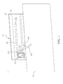
- FIG. 1 is a structural drawing of a communication electronic device with an antenna structure 1 according to a first exemplary embodiment of the present invention.
- FIG. 2 is a diagram illustrating the input impedance of the communication electronic device with the antenna structure 1 according to the first exemplary embodiment of the present invention.
- the communication electronic device with the antenna structure 1 comprises a ground element 10 and an antenna element 11.
- the antenna element 11 is disposed on a dielectric substrate 12, and comprises a first radiation portion 13, a second radiation portion 14 and a spiral metal line 15.
- a first end of the first radiation portion 13 is a feeding point 131 of the antenna element 11, the signal is fed through a coaxial line 16 connected thereto.
- a second end of the first radiation portion 13 is an open end 132.
- One end 141 of the second radiation portion 14 is electrically coupled to the ground element 10.
- a length of the second radiation portion 14 is greater than that of the first radiation portion 13.
- the second radiation portion 14 is extended around the open end 132 of the first radiation portion 13.
- a first end 151 of the spiral metal line 15 is electrically coupled to the first radiation portion 13.
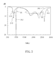
- the spiral metal line 15 can contribute a parallel resonance 43 (as shown in FIG. 2 ) at a frequency outside a lower band 31 (shown in FIG. 5 ) of the antenna element 11.
- the parallel resonance 43 generates an additional resonant mode 312 (as shown in FIG. 5 ) in the lower band 31 such that an operating bandwidth of the antenna in the lower band 31 can be increased.
- the first radiation portion 13 is implemented using a monopole antenna.
- a second end 152 of the spiral metal line 15 is an open end and spirals inward.
- the spiral metal line 15 spirals in a rectangular shape.
- FIG. 3 is a structural drawing of a conventional communication electronic device with a conventional antenna structure 2 thereof.
- FIG. 4 is a diagram illustrating input impedance of the conventional communication electronic device with the conventional antenna structure 2.
- the communication electronic device and the antenna structure 2 comprise a ground element 20 and an antenna element 21.
- the antenna element 21 is disposed on a dielectric substrate 22, and comprises a first radiation portion 23 and a second radiation portion 24.
- a first end of the first radiation portion 23 is a feeding point 231 of the antenna element 21, and the signal is fed through a coaxial line 26 connected thereto.
- the second end of the first radiation portion 23 is an open end 232.
- the first radiation portion 23 can contribute a resonant mode (as shown in FIG. 3 ) at a higher band 32 of the antenna element 21.
- a first end 241 of the second radiation portion 24 is electrically coupled to the ground element 20.
- a length of the second radiation portion 24 is greater than that of the first radiation portion 23.
- the second radiation portion 24 is extended around the open end 232 of the first radiation portion 23.
- the second radiation portion 24 can contribute a resonant mode (e.g. the resonant mode 313 shown in FIG. 5 ) at a lower band 31 of the antenna element 21.
- the bandwidth of the resonant mode is narrow, which fails to cover multi-band operation.
- the antenna element 11 of the communication electronic device with the antenna structure 1 includes the spiral metal line 15. With the spiral metal line 15, a parallel resonance can be generated at a frequency outside the lower band of the antenna element 11. The parallel resonance will in turn generate a resonant mode in the lower band, which can be further combined with the original resonant mode of the second radiation portion, thereby increasing the operating bandwidth of the antenna element 11.
- FIG. 5 is a diagram illustrating return loss of the communication electronic device 1 as shown in FIG. 1 and the conventional communication electronic device 2 as shown in FIG. 3 .
- the first radiation portion 13 of the communication electronic device 1 generates at least one resonant mode in a second (higher frequency) operating band 32.
- the second radiation portion 14 of the communication electronic device 1 generates at least one resonant mode in the first (lower frequency) operating band 31.
- FIG. 2 is a diagram illustrating the input impedance of the communication electronic device with the antenna structure 1.
- FIG. 4 is a diagram illustrating the input impedance of the conventional communication electronic device with the antenna structure 2.
- FIG. 5 is a diagram illustrating return loss of the communication electronic device 1 of FIG. 1 and the conventional communication electronic device 2 of FIG. 3 .
- the input impedance of the communication electronic device 1 has a real part 41 and an imaginary part 42.
- the input impedance of the communication electronic device 2 has a real part 51 and an imaginary part 52.
- a length of the ground element 20 is about 150 mm and a width of the ground element 20 is about 200 mm; a length of the dielectric substrate 22 is about 40 mm, a width of the dielectric substrate 22 is about 12 mm and a thickness of the dielectric substrate 22 is about 0.8 mm.
- a length of the first radiation portion 23 is about 30 mm and a length of second radiation portion 24 is about 75 mm. The second radiation portion 24 can cause a quarter-wavelength resonant mode 313.
- the bandwidth of the resonant mode 313 will be narrow and fail to cover multi-band operation with the 6-dB return-loss definition (which is the design specification widely used for the mobile communication device antennas).
- the sizes of the elements are chosen as the similar sizes of the elements of the conventional communication electronic device 2 shown in FIG. 3 .
- a length of the spiral metal line 15 is about 60 mm.
- the second radiation portion 14 can cause the quarter-wavelength resonant mode 311 and the higher-order resonant mode.
- the spiral metal line 15 can contribute a parallel resonance 43 (having a center frequency at about 1.1 GHz) at a frequency outside the lower band 31 of the antenna element 11.
- the parallel resonance 43 generates an additional resonance around the resonant mode 311 (e.g. the zero imaginary part of the impedance as shown in FIG. 2 ), thereby generating a resonant mode 312.
- the resonant mode 312 and the resonant mode 311 generated by the second radiation portion 14 collectively generate the first (lower frequency) operating band (e.g. the operating band 31 shown in FIG. 5 ).
- the first radiation portion 13 can cause a quarter-wavelength resonant mode.
- the quarter-wavelength resonant mode and the higher-order resonant mode generated by the second radiation portion 14 collectively generate the second (higher frequency) operating band (e.g. the operating band 32 shown in FIG. 5 ).
- the first operating band 31 covers at least the dual-band operation of GSM850/900 (from about 824 to 960 MHz).
- the second operating band 32 covers at least the triple-band operation of GSM1800/1900/UMTS (from about 1710 to 2170 MHz).
- the operating bandwidth of the communication electronic device 1 is significantly increased by the spiral metal line 15, thereby allowing the first operating band 31 to achieve multi-band operation.
- FIG. 6 is a structural drawing of a communication electronic device with an antenna structure 6 thereof according to a second exemplary embodiment of the present invention.
- the antenna structure is basically similar to the antenna structure of the first exemplary embodiment.
- the difference between these two exemplary embodiments is that structures of the antenna element 61 and the spiral metal line 65 are changed.
- the spiral metal line 65 can spiral in circular shapes. Since the antenna structure of the second exemplary embodiment is similar to that of the first exemplary embodiment, effects of the second exemplary embodiment are also similar to those of the first exemplary embodiment.
- FIG. 7 is a structural drawing of a communication electronic device with an antenna structure 7 according to a third exemplary embodiment of the present invention.
- the antenna structure of the third exemplary embodiment is basically similar to the antenna structure of the first exemplary embodiment.
- the difference between the antenna structures of these two exemplary embodiments is that the position where the antenna element 71 and the spiral metal line 75 are electrically coupled is changed.
- the spiral metal line 75 is adjusted to determine the center frequency of the parallel resonance generated by the spiral metal line 75. Since the antenna structure of the third exemplary embodiment is similar to that of the first exemplary embodiment, effects of the third exemplary embodiment are also similar to those of the first exemplary embodiment.
Landscapes
- Engineering & Computer Science (AREA)
- Computer Networks & Wireless Communication (AREA)
- Details Of Aerials (AREA)
- Support Of Aerials (AREA)
Applications Claiming Priority (1)
| Application Number | Priority Date | Filing Date | Title |
|---|---|---|---|
| TW100148862A TWI488358B (zh) | 2011-12-27 | 2011-12-27 | 通訊電子裝置及其天線結構 |
Publications (2)
| Publication Number | Publication Date |
|---|---|
| EP2610962A2 true EP2610962A2 (fr) | 2013-07-03 |
| EP2610962A3 EP2610962A3 (fr) | 2013-10-23 |
Family
ID=46197041
Family Applications (1)
| Application Number | Title | Priority Date | Filing Date |
|---|---|---|---|
| EP12168895.6A Withdrawn EP2610962A3 (fr) | 2011-12-27 | 2012-05-22 | Dispositif électronique de communication et sa structure d'antenne |
Country Status (3)
| Country | Link |
|---|---|
| US (1) | US8922449B2 (fr) |
| EP (1) | EP2610962A3 (fr) |
| TW (1) | TWI488358B (fr) |
Cited By (1)
| Publication number | Priority date | Publication date | Assignee | Title |
|---|---|---|---|---|
| WO2017001937A1 (fr) * | 2015-01-07 | 2017-01-05 | Galtronics Corporation Ltd. | Structure d'antenne compacte |
Families Citing this family (14)
| Publication number | Priority date | Publication date | Assignee | Title |
|---|---|---|---|---|
| CN104577303A (zh) * | 2013-10-17 | 2015-04-29 | 启碁科技股份有限公司 | 天线 |
| TWI451629B (zh) * | 2013-11-04 | 2014-09-01 | Quanta Comp Inc | 天線結構 |
| TWI509883B (zh) * | 2013-12-06 | 2015-11-21 | Univ Nat Kaohsiung Marine | 平面式多頻單極天線 |
| CN104795624A (zh) * | 2014-01-17 | 2015-07-22 | 台湾立讯精密有限公司 | 全频带天线 |
| TWI501464B (zh) * | 2014-03-05 | 2015-09-21 | Quanta Comp Inc | 行動裝置 |
| CN206907920U (zh) * | 2016-12-14 | 2018-01-19 | 深圳市道通智能航空技术有限公司 | 一种双频段微带天线及应用该天线的无人机 |
| CN112821037B (zh) | 2019-11-15 | 2022-09-02 | 英业达科技有限公司 | 多频天线 |
| TWI725642B (zh) * | 2019-11-29 | 2021-04-21 | 英業達股份有限公司 | 多頻天線 |
| CN112968270B (zh) * | 2019-12-13 | 2022-09-23 | 华为技术有限公司 | 双频天线及通讯设备 |
| TWI723833B (zh) * | 2020-04-01 | 2021-04-01 | 啟碁科技股份有限公司 | 天線結構 |
| CN114069207B (zh) * | 2020-07-29 | 2023-08-22 | 北京小米移动软件有限公司 | 天线结构和电子设备 |
| CN112736454B (zh) * | 2020-12-25 | 2023-04-07 | RealMe重庆移动通信有限公司 | 天线组件及电子设备 |
| WO2024050994A1 (fr) * | 2022-09-08 | 2024-03-14 | 昆山睿翔讯通通信技术有限公司 | Antenne de terminal mobile et terminal mobile |
| CN115603036B (zh) * | 2022-09-08 | 2025-07-11 | 昆山睿翔讯通通信技术有限公司 | 一种移动终端天线及移动终端 |
Citations (1)
| Publication number | Priority date | Publication date | Assignee | Title |
|---|---|---|---|---|
| US7978141B2 (en) | 2008-05-05 | 2011-07-12 | Acer Incorporated | Couple-fed multi-band loop antenna |
Family Cites Families (7)
| Publication number | Priority date | Publication date | Assignee | Title |
|---|---|---|---|---|
| CN1386312A (zh) | 2000-08-04 | 2002-12-18 | 松下电器产业株式会社 | 天线装置及使用该天线装置的无线通信机 |
| AU2002333900A1 (en) * | 2002-09-10 | 2004-04-30 | Fractus, S.A. | Coupled multiband antennas |
| US20060197538A1 (en) * | 2005-03-07 | 2006-09-07 | Nokia Corporation | Self-test method for antennas |
| US7760146B2 (en) * | 2005-03-24 | 2010-07-20 | Nokia Corporation | Internal digital TV antennas for hand-held telecommunications device |
| WO2007128340A1 (fr) * | 2006-05-04 | 2007-11-15 | Fractus, S.A. | DISPOSITIF PORTABLE SANS FIL COMPRENANT UN RÉCEPTEUR DE radioDIFFUSION INTERNE |
| US8618990B2 (en) * | 2011-04-13 | 2013-12-31 | Pulse Finland Oy | Wideband antenna and methods |
| KR101480555B1 (ko) * | 2008-06-19 | 2015-01-09 | 삼성전자주식회사 | 휴대용 단말기의 안테나 장치 |
-
2011
- 2011-12-27 TW TW100148862A patent/TWI488358B/zh active
-
2012
- 2012-04-18 US US13/449,318 patent/US8922449B2/en active Active
- 2012-05-22 EP EP12168895.6A patent/EP2610962A3/fr not_active Withdrawn
Patent Citations (1)
| Publication number | Priority date | Publication date | Assignee | Title |
|---|---|---|---|---|
| US7978141B2 (en) | 2008-05-05 | 2011-07-12 | Acer Incorporated | Couple-fed multi-band loop antenna |
Cited By (2)
| Publication number | Priority date | Publication date | Assignee | Title |
|---|---|---|---|---|
| WO2017001937A1 (fr) * | 2015-01-07 | 2017-01-05 | Galtronics Corporation Ltd. | Structure d'antenne compacte |
| CN107534211A (zh) * | 2015-01-07 | 2018-01-02 | 盖尔创尼克斯有限公司 | 小型天线结构 |
Also Published As
| Publication number | Publication date |
|---|---|
| US8922449B2 (en) | 2014-12-30 |
| TW201328016A (zh) | 2013-07-01 |
| US20130162494A1 (en) | 2013-06-27 |
| EP2610962A3 (fr) | 2013-10-23 |
| TWI488358B (zh) | 2015-06-11 |
Similar Documents
| Publication | Publication Date | Title |
|---|---|---|
| EP2610962A2 (fr) | Dispositif électronique de communication et sa structure d'antenne | |
| US10819031B2 (en) | Printed circuit board antenna and terminal | |
| US6614400B2 (en) | Antenna | |
| US7616158B2 (en) | Multi mode antenna system | |
| US6552686B2 (en) | Internal multi-band antenna with improved radiation efficiency | |
| CN102075205B (zh) | 移动通讯装置 | |
| CN1173432C (zh) | 天线系统中用于连接到接地装置的接地延伸结构,和具有这种接地结构的天线系统和移动天线装置 | |
| US6734825B1 (en) | Miniature built-in multiple frequency band antenna | |
| US9276320B2 (en) | Multi-band antenna | |
| EP2246935A1 (fr) | Structure d'antenne multi-boucles et appareil électronique portatif utilisant cette structure d'antenne | |
| EP2511978B1 (fr) | Dispositif de communication mobile et structure d'antenne correspondante | |
| EP2381529B1 (fr) | Structures de communication incluant des antennes avec des branches d'antennes séparées couplées pour alimenter et mettre à la terre des conducteurs | |
| US8593354B2 (en) | Multi-band antenna | |
| US20080231532A1 (en) | Multi-band slot-strip antenna | |
| EP2509158B1 (fr) | Dispositif électronique de communication et sa structure d'antenne | |
| EP2575207B1 (fr) | Dispositif électronique de communication et sa structure d'antenne | |
| CN106207372A (zh) | 移动装置及其制造方法 | |
| WO2007107101A1 (fr) | Antenne interne à alimentation unique multibande pour terminaux de communication mobiles | |
| US20130225234A1 (en) | Mobile device and wideband antenna structure therein | |
| CN102099962A (zh) | 天线结构 | |
| EP1852939A1 (fr) | Dispositif portable sans fil | |
| CN100468861C (zh) | 多频带无线电天线 | |
| EP1678783B1 (fr) | Antennes multibandes et appareil de radio les contenant | |
| CN101283478A (zh) | 设置有陷波器的天线结构 | |
| Elfergani et al. | Dual-band printed folded dipole balanced antenna for 700/2600MHz LTE bands |
Legal Events
| Date | Code | Title | Description |
|---|---|---|---|
| PUAI | Public reference made under article 153(3) epc to a published international application that has entered the european phase |
Free format text: ORIGINAL CODE: 0009012 |
|
| AK | Designated contracting states |
Kind code of ref document: A2 Designated state(s): AL AT BE BG CH CY CZ DE DK EE ES FI FR GB GR HR HU IE IS IT LI LT LU LV MC MK MT NL NO PL PT RO RS SE SI SK SM TR |
|
| AX | Request for extension of the european patent |
Extension state: BA ME |
|
| PUAL | Search report despatched |
Free format text: ORIGINAL CODE: 0009013 |
|
| AK | Designated contracting states |
Kind code of ref document: A3 Designated state(s): AL AT BE BG CH CY CZ DE DK EE ES FI FR GB GR HR HU IE IS IT LI LT LU LV MC MK MT NL NO PL PT RO RS SE SI SK SM TR |
|
| AX | Request for extension of the european patent |
Extension state: BA ME |
|
| RIC1 | Information provided on ipc code assigned before grant |
Ipc: H01Q 1/38 20060101ALI20130913BHEP Ipc: H01Q 1/24 20060101AFI20130913BHEP Ipc: H01Q 9/40 20060101ALI20130913BHEP Ipc: H01Q 5/00 20060101ALI20130913BHEP Ipc: H01Q 9/42 20060101ALI20130913BHEP |
|
| STAA | Information on the status of an ep patent application or granted ep patent |
Free format text: STATUS: THE APPLICATION IS DEEMED TO BE WITHDRAWN |
|
| 18D | Application deemed to be withdrawn |
Effective date: 20140424 |