EP2586568A2 - Procédé et appareil de polissage - Google Patents
Procédé et appareil de polissage Download PDFInfo
- Publication number
- EP2586568A2 EP2586568A2 EP12007343.2A EP12007343A EP2586568A2 EP 2586568 A2 EP2586568 A2 EP 2586568A2 EP 12007343 A EP12007343 A EP 12007343A EP 2586568 A2 EP2586568 A2 EP 2586568A2
- Authority
- EP
- European Patent Office
- Prior art keywords
- polishing
- substrate
- silicon layer
- thickness
- infrared ray
- Prior art date
- Legal status (The legal status is an assumption and is not a legal conclusion. Google has not performed a legal analysis and makes no representation as to the accuracy of the status listed.)
- Withdrawn
Links
Images








Classifications
-
- H—ELECTRICITY
- H10—SEMICONDUCTOR DEVICES; ELECTRIC SOLID-STATE DEVICES NOT OTHERWISE PROVIDED FOR
- H10P—GENERIC PROCESSES OR APPARATUS FOR THE MANUFACTURE OR TREATMENT OF DEVICES COVERED BY CLASS H10
- H10P95/00—Generic processes or apparatus for manufacture or treatments not covered by the other groups of this subclass
- H10P95/06—Planarisation of inorganic insulating materials
-
- H—ELECTRICITY
- H10—SEMICONDUCTOR DEVICES; ELECTRIC SOLID-STATE DEVICES NOT OTHERWISE PROVIDED FOR
- H10P—GENERIC PROCESSES OR APPARATUS FOR THE MANUFACTURE OR TREATMENT OF DEVICES COVERED BY CLASS H10
- H10P74/00—Testing or measuring during manufacture or treatment of wafers, substrates or devices
- H10P74/23—Testing or measuring during manufacture or treatment of wafers, substrates or devices characterised by multiple measurements, corrections, marking or sorting processes
- H10P74/238—Testing or measuring during manufacture or treatment of wafers, substrates or devices characterised by multiple measurements, corrections, marking or sorting processes comprising acting in response to an ongoing measurement without interruption of processing, e.g. endpoint detection or in-situ thickness measurement
-
- B—PERFORMING OPERATIONS; TRANSPORTING
- B24—GRINDING; POLISHING
- B24B—MACHINES, DEVICES, OR PROCESSES FOR GRINDING OR POLISHING; DRESSING OR CONDITIONING OF ABRADING SURFACES; FEEDING OF GRINDING, POLISHING, OR LAPPING AGENTS
- B24B37/00—Lapping machines or devices; Accessories
- B24B37/005—Control means for lapping machines or devices
- B24B37/013—Devices or means for detecting lapping completion
-
- B—PERFORMING OPERATIONS; TRANSPORTING
- B24—GRINDING; POLISHING
- B24B—MACHINES, DEVICES, OR PROCESSES FOR GRINDING OR POLISHING; DRESSING OR CONDITIONING OF ABRADING SURFACES; FEEDING OF GRINDING, POLISHING, OR LAPPING AGENTS
- B24B37/00—Lapping machines or devices; Accessories
- B24B37/11—Lapping tools
- B24B37/20—Lapping pads for working plane surfaces
-
- B—PERFORMING OPERATIONS; TRANSPORTING
- B24—GRINDING; POLISHING
- B24B—MACHINES, DEVICES, OR PROCESSES FOR GRINDING OR POLISHING; DRESSING OR CONDITIONING OF ABRADING SURFACES; FEEDING OF GRINDING, POLISHING, OR LAPPING AGENTS
- B24B49/00—Measuring or gauging equipment for controlling the feed movement of the grinding tool or work; Arrangements of indicating or measuring equipment, e.g. for indicating the start of the grinding operation
- B24B49/02—Measuring or gauging equipment for controlling the feed movement of the grinding tool or work; Arrangements of indicating or measuring equipment, e.g. for indicating the start of the grinding operation according to the instantaneous size and required size of the workpiece acted upon, the measuring or gauging being continuous or intermittent
- B24B49/04—Measuring or gauging equipment for controlling the feed movement of the grinding tool or work; Arrangements of indicating or measuring equipment, e.g. for indicating the start of the grinding operation according to the instantaneous size and required size of the workpiece acted upon, the measuring or gauging being continuous or intermittent involving measurement of the workpiece at the place of grinding during grinding operation
-
- B—PERFORMING OPERATIONS; TRANSPORTING
- B24—GRINDING; POLISHING
- B24B—MACHINES, DEVICES, OR PROCESSES FOR GRINDING OR POLISHING; DRESSING OR CONDITIONING OF ABRADING SURFACES; FEEDING OF GRINDING, POLISHING, OR LAPPING AGENTS
- B24B49/00—Measuring or gauging equipment for controlling the feed movement of the grinding tool or work; Arrangements of indicating or measuring equipment, e.g. for indicating the start of the grinding operation
- B24B49/12—Measuring or gauging equipment for controlling the feed movement of the grinding tool or work; Arrangements of indicating or measuring equipment, e.g. for indicating the start of the grinding operation involving optical means
-
- H—ELECTRICITY
- H10—SEMICONDUCTOR DEVICES; ELECTRIC SOLID-STATE DEVICES NOT OTHERWISE PROVIDED FOR
- H10P—GENERIC PROCESSES OR APPARATUS FOR THE MANUFACTURE OR TREATMENT OF DEVICES COVERED BY CLASS H10
- H10P52/00—Grinding, lapping or polishing of wafers, substrates or parts of devices
-
- H—ELECTRICITY
- H10—SEMICONDUCTOR DEVICES; ELECTRIC SOLID-STATE DEVICES NOT OTHERWISE PROVIDED FOR
- H10P—GENERIC PROCESSES OR APPARATUS FOR THE MANUFACTURE OR TREATMENT OF DEVICES COVERED BY CLASS H10
- H10P52/00—Grinding, lapping or polishing of wafers, substrates or parts of devices
- H10P52/40—Chemomechanical polishing [CMP]
- H10P52/402—Chemomechanical polishing [CMP] of semiconductor materials
-
- H—ELECTRICITY
- H10—SEMICONDUCTOR DEVICES; ELECTRIC SOLID-STATE DEVICES NOT OTHERWISE PROVIDED FOR
- H10P—GENERIC PROCESSES OR APPARATUS FOR THE MANUFACTURE OR TREATMENT OF DEVICES COVERED BY CLASS H10
- H10P72/00—Handling or holding of wafers, substrates or devices during manufacture or treatment thereof
- H10P72/04—Apparatus for manufacture or treatment
- H10P72/0428—Apparatus for mechanical treatment or grinding or cutting
-
- H—ELECTRICITY
- H10—SEMICONDUCTOR DEVICES; ELECTRIC SOLID-STATE DEVICES NOT OTHERWISE PROVIDED FOR
- H10P—GENERIC PROCESSES OR APPARATUS FOR THE MANUFACTURE OR TREATMENT OF DEVICES COVERED BY CLASS H10
- H10P72/00—Handling or holding of wafers, substrates or devices during manufacture or treatment thereof
- H10P72/06—Apparatus for monitoring, sorting, marking, testing or measuring
-
- H—ELECTRICITY
- H10—SEMICONDUCTOR DEVICES; ELECTRIC SOLID-STATE DEVICES NOT OTHERWISE PROVIDED FOR
- H10P—GENERIC PROCESSES OR APPARATUS FOR THE MANUFACTURE OR TREATMENT OF DEVICES COVERED BY CLASS H10
- H10P74/00—Testing or measuring during manufacture or treatment of wafers, substrates or devices
- H10P74/20—Testing or measuring during manufacture or treatment of wafers, substrates or devices characterised by the properties tested or measured, e.g. structural or electrical properties
- H10P74/203—Structural properties, e.g. testing or measuring thicknesses, line widths, warpage, bond strengths or physical defects
Definitions
- the top ring 110 and the polishing table 101 rotate as indicated by arrows.
- the top ring 110 presses the wafer W against the polishing pad 110, while the slurry supply unit 115 supplies the polishing liquid onto the polishing pad 110.
- the wafer W is polished by sliding contact with the polishing pad 110 in the presence of the polishing liquid.
- the film-thickness measuring device 120 rotates together with the polishing table 101 and measures the film thickness while sweeping a surface of the wafer W. Polishing of the wafer W is terminated when the film thickness has reached the predetermined target value.
- the film-thickness measuring device using the infrared ray can measure the thickness of the silicon layer.
- the film-thickness measuring device incorporated in the CMP apparatus may fail to measure the thickness if there is a variation in the thickness of the silicon layer because it measures the thickness of the silicon layer while the device itself is moving as shown in FIG. 1 .
- the silicon layers that have been polished in the above-mentioned BSI fabrication process and the TSV fabrication process have a polished surface with low flatness, which is likely to cause the failure of measurement.
- One possible solution to such measurement failure is to shorten a measuring time per one measuring operation. However, in this case, a quantity of the reflected infrared ray is reduced and as a result S/N ratio is lowered. This makes it difficult to achieve accurate measurement.
- the silicon layer is scraped away every time the polishing table makes one revolution, it is impossible to measure the thickness at the same position under the same conditions.
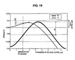
- the polishing monitoring unit is configured to calculate relative reflectance by dividing the measured intensity of the light by predetermined reference intensity, produce spectral waveform representing relationship between the relative reflectance and wavelength of the light, perform a Fourier transform process on the spectral waveform to obtain relationship between thickness of the film and strength of frequency component and to determine the thickness of the film and a corresponding strength of frequency component, identify the determined thickness of the film as a reliable measured value if an absolute value of a difference between a strength of the frequency component at a predetermined observation thickness and the determined strength of frequency component is larger than a predetermined threshold value, and determine the polishing end point of the substrate based on a point of time when the reliable measured value has reached the predetermined target value.
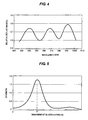
- FIG. 4 is a diagram showing spectral waveform created by the first processor 15A.
- horizontal axis represents wavelength of the infrared ray reflected from the wafer
- vertical axis represents relative reflectance derived from the intensity of the infrared ray.
- the relative reflectance is an index that represents the reflection intensity of the infrared ray. More specifically, the relative reflectance is a ratio of the intensity of the infrared ray to a predetermined corresponding reference intensity.
- the actually measured intensity By dividing intensities of the infrared ray (i.e., the actually measured intensity) at the respective wavelengths by predetermined reference intensities, unwanted noise, such as a variation in the intensity inherent in an optical system or light source of the apparatus, are removed from the actually measured intensity. As a result, the spectral waveform reflecting only the thickness information of the silicon layer can be obtained.
- the measured value with a low strength tends to differ greatly from other measured values.
- the measured value with a low strength of the frequency component does not represent the actual thickness of the silicon layer accurately.
- the measured value with a lower strength of the frequency component than a predetermined threshold value is removed from measurement data, so that the second processor 15B obtains monitoring data that contains only reliable measured values.
- Symbol ⁇ shown in FIG. 7 represents measured value with the strength equal to or more than the predetermined threshold value
- symbol ⁇ represents measured value with the strength lower than the predetermined threshold value.
- the monitoring data consists of the measured values with the symbol ⁇ .
- FIG. 11 is a diagram showing polishing profiles before and after polishing of the wafer.
- Vertical axis represents the thickness of the silicon layer
- horizontal axis represents radial position on the wafer.
- the variation in the measured value at the central region of the wafer is relatively small.
- the measured values obtained in the central region of the wafer are reliable ones. Therefore, it is preferable to determine the polishing end point by using only the measured values obtained in the central region of the wafer.
- the present invention is not limited to this example.
- the measured values obtained in regions other than the central region of the wafer can also be used. For example, it is possible to determine the polishing end point using only the measured values obtained in a peripheral region of the wafer. Further, it is also possible to use the measured values obtained in preselected regions (e.g., the central region and the peripheral region of the wafer shown in FIG. 6 ).
- FIG. 17 is a diagram showing cumulative frequency polygon graph created from the histogram shown in FIG. 16 .
- Vertical axis represents cumulative value (expressed as percentage) of frequency of appearance of the strength of the frequency component.
- a light emitting diode can be used as the light source 40.
- the infrared ray to be emitted from the light source 40 is preferably the near infrared ray having the wavelength in the range of 920 nm to 980 nm. Since the near infrared ray in this wavelength range is hardly absorbed into the water as compared with infrared ray having longer wavelength, more precise measurement can be realized.
- the optical fiber 41 and the optical fiber 12 are arranged in parallel with each other. The tip ends of the optical fiber 41 and the optical fiber 12 are approximately perpendicular to the surface of the wafer W, so that the optical fiber 41 directs the infrared ray to the surface of the wafer W perpendicularly.
- the above-described silicon layer may be a silicon substrate itself.
- the present invention is applicable to polishing (or grinding) of the silicon substrate itself.
- the present invention can be applied to a process of grinding a back-side surface of the silicon substrate.
- An apparatus for polishing (or grinding) the silicon substrate uses a bonded abrasive (or grinding stone) as the polishing tool, instead of the polishing pad 22.
Landscapes
- Engineering & Computer Science (AREA)
- Mechanical Engineering (AREA)
- Mechanical Treatment Of Semiconductor (AREA)
- Finish Polishing, Edge Sharpening, And Grinding By Specific Grinding Devices (AREA)
- Constituent Portions Of Griding Lathes, Driving, Sensing And Control (AREA)
Applications Claiming Priority (2)
| Application Number | Priority Date | Filing Date | Title |
|---|---|---|---|
| JP2011235024 | 2011-10-26 | ||
| JP2012222682A JP6005467B2 (ja) | 2011-10-26 | 2012-10-05 | 研磨方法および研磨装置 |
Publications (2)
| Publication Number | Publication Date |
|---|---|
| EP2586568A2 true EP2586568A2 (fr) | 2013-05-01 |
| EP2586568A3 EP2586568A3 (fr) | 2017-10-04 |
Family
ID=47429493
Family Applications (1)
| Application Number | Title | Priority Date | Filing Date |
|---|---|---|---|
| EP12007343.2A Withdrawn EP2586568A3 (fr) | 2011-10-26 | 2012-10-25 | Procédé et appareil de polissage |
Country Status (6)
| Country | Link |
|---|---|
| US (2) | US9561577B2 (fr) |
| EP (1) | EP2586568A3 (fr) |
| JP (1) | JP6005467B2 (fr) |
| KR (2) | KR101884475B1 (fr) |
| CN (1) | CN103072072B (fr) |
| TW (2) | TWI674170B (fr) |
Families Citing this family (27)
| Publication number | Priority date | Publication date | Assignee | Title |
|---|---|---|---|---|
| JP6105371B2 (ja) | 2013-04-25 | 2017-03-29 | 株式会社荏原製作所 | 研磨方法および研磨装置 |
| US20150022658A1 (en) * | 2013-07-16 | 2015-01-22 | University Of North Carolina At Charlotte | Noise reduction techniques, fractional bi-spectrum and fractional cross-correlation, and applications |
| WO2015038850A2 (fr) * | 2013-09-12 | 2015-03-19 | Sio2 Medical Products, Inc. | Analyse par spectrométrie infrarouge sélective, rapide et non destructive de revêtements organiques sur articles moulés |
| CN103489223A (zh) * | 2013-09-29 | 2014-01-01 | 华南理工大学 | 一种面向3d封装ic的3d断层扫描成像方法 |
| US9349661B2 (en) | 2014-01-23 | 2016-05-24 | Globalfoundries Inc. | Wafer thinning endpoint detection for TSV technology |
| US20160013085A1 (en) * | 2014-07-10 | 2016-01-14 | Applied Materials, Inc. | In-Situ Acoustic Monitoring of Chemical Mechanical Polishing |
| JP6404172B2 (ja) | 2015-04-08 | 2018-10-10 | 株式会社荏原製作所 | 膜厚測定方法、膜厚測定装置、研磨方法、および研磨装置 |
| JP1544543S (fr) * | 2015-05-14 | 2019-02-18 | ||
| JP6473050B2 (ja) | 2015-06-05 | 2019-02-20 | 株式会社荏原製作所 | 研磨装置 |
| JP6649135B2 (ja) * | 2016-03-10 | 2020-02-19 | 株式会社東京精密 | ウェハ加工装置及びウェハ加工方法 |
| KR102539142B1 (ko) | 2016-09-05 | 2023-06-01 | 삼성전자주식회사 | 스펙트럼 분석 장치와 방법, 및 혈당 측정 장치 |
| JP6948868B2 (ja) * | 2017-07-24 | 2021-10-13 | 株式会社荏原製作所 | 研磨装置および研磨方法 |
| JP6860451B2 (ja) * | 2017-09-05 | 2021-04-14 | 株式会社荏原製作所 | 機能性チップを備える基板を研磨する方法 |
| CN107520740A (zh) * | 2017-09-18 | 2017-12-29 | 北京半导体专用设备研究所(中国电子科技集团公司第四十五研究所) | 一种化学机械抛光中光谱终点的检测方法、装置及系统 |
| JP7403213B2 (ja) * | 2017-10-31 | 2023-12-22 | 株式会社荏原製作所 | 研磨装置、及び研磨方法 |
| KR102435764B1 (ko) * | 2017-11-17 | 2022-08-24 | 삼성디스플레이 주식회사 | 레이저 결정화 돌기의 제거 장치 및 방법 |
| JP7118660B2 (ja) * | 2018-02-19 | 2022-08-16 | 三菱重工業株式会社 | 差動トランス式変位計の断線検知システム、差動トランス式変位計、及び断線検知方法 |
| US11701749B2 (en) | 2018-03-13 | 2023-07-18 | Applied Materials, Inc. | Monitoring of vibrations during chemical mechanical polishing |
| US11315232B2 (en) | 2018-10-22 | 2022-04-26 | Applied Materials, Inc. | Residue detection using a luminance histogram |
| JP7253458B2 (ja) | 2019-06-27 | 2023-04-06 | 株式会社荏原製作所 | 光学式膜厚測定装置の最適な動作レシピを決定する方法、装置、およびシステム |
| JP7339811B2 (ja) * | 2019-08-27 | 2023-09-06 | 株式会社荏原製作所 | リテーナリングに局所荷重を伝達するローラーの異常検出方法および研磨装置 |
| JP7460411B2 (ja) * | 2020-03-24 | 2024-04-02 | 株式会社Screenホールディングス | 基板処理装置及び基板処理方法 |
| JP7503418B2 (ja) * | 2020-05-14 | 2024-06-20 | 株式会社荏原製作所 | 膜厚測定装置、研磨装置及び膜厚測定方法 |
| JP7389718B2 (ja) * | 2020-06-29 | 2023-11-30 | 株式会社荏原製作所 | 研磨方法、研磨装置、およびプログラムを記録したコンピュータ読み取り可能な記録媒体 |
| US20220176513A1 (en) * | 2020-11-24 | 2022-06-09 | Ebara Corporation | Polishing method, polishing monitoring method and polishing monitoring apparatus for workpiece |
| CN114029790B (zh) * | 2021-11-25 | 2023-04-07 | 北京晶亦精微科技股份有限公司 | 一种晶圆研磨方法 |
| CN116619233B (zh) * | 2023-04-28 | 2026-03-31 | 北京石晶光电科技股份有限公司 | 一种晶片双面研磨厚度精确控制方法 |
Family Cites Families (22)
| Publication number | Priority date | Publication date | Assignee | Title |
|---|---|---|---|---|
| US5499733A (en) * | 1992-09-17 | 1996-03-19 | Luxtron Corporation | Optical techniques of measuring endpoint during the processing of material layers in an optically hostile environment |
| JPH10125634A (ja) | 1996-10-19 | 1998-05-15 | Nikon Corp | 研磨装置 |
| JP4460659B2 (ja) * | 1997-10-22 | 2010-05-12 | 株式会社ルネサステクノロジ | 薄膜の膜厚計測方法及びその装置並びにそれを用いた薄膜デバイスの製造方法及びその製造装置 |
| JP3854056B2 (ja) | 1999-12-13 | 2006-12-06 | 株式会社荏原製作所 | 基板膜厚測定方法、基板膜厚測定装置、基板処理方法及び基板処理装置 |
| US6511363B2 (en) * | 2000-12-27 | 2003-01-28 | Tokyo Seimitsu Co., Ltd. | Polishing end point detecting device for wafer polishing apparatus |
| US6812478B2 (en) * | 2001-03-19 | 2004-11-02 | Lam Research Corporation | In-situ detection of thin-metal interface using optical interference via a dynamically updated reference |
| JP4131632B2 (ja) * | 2001-06-15 | 2008-08-13 | 株式会社荏原製作所 | ポリッシング装置及び研磨パッド |
| JP2003249472A (ja) * | 2002-02-26 | 2003-09-05 | Hitachi Ltd | 膜厚計測方法および膜厚計測装置および薄膜デバイスの製造方法 |
| JP4542324B2 (ja) | 2002-10-17 | 2010-09-15 | 株式会社荏原製作所 | 研磨状態監視装置及びポリッシング装置 |
| US6895360B2 (en) * | 2002-12-17 | 2005-05-17 | Taiwan Semiconductor Manufacturing Co., Ltd. | Method to measure oxide thickness by FTIR to improve an in-line CMP endpoint determination |
| JP4464642B2 (ja) * | 2003-09-10 | 2010-05-19 | 株式会社荏原製作所 | 研磨状態監視装置、研磨状態監視方法、研磨装置及び研磨方法 |
| JP4501633B2 (ja) * | 2004-10-28 | 2010-07-14 | ソニー株式会社 | 固体撮像素子とその製造方法 |
| US20070148792A1 (en) * | 2005-12-27 | 2007-06-28 | Marx David S | Wafer measurement system and apparatus |
| JP2008083059A (ja) * | 2006-09-26 | 2008-04-10 | David S Marx | ウェーハの測定システム及び測定装置 |
| TWI422798B (zh) * | 2006-10-06 | 2014-01-11 | 荏原製作所股份有限公司 | 加工終點檢測方法、研磨方法及研磨裝置 |
| JP2009050944A (ja) | 2007-08-24 | 2009-03-12 | Disco Abrasive Syst Ltd | 基板の厚さ測定方法および基板の加工装置 |
| JP5339791B2 (ja) * | 2008-06-30 | 2013-11-13 | 株式会社東京精密 | 研磨終点検出方法及び研磨装置 |
| JP2010093147A (ja) * | 2008-10-10 | 2010-04-22 | Ebara Corp | 研磨進捗監視方法および研磨装置 |
| US8388408B2 (en) * | 2008-10-10 | 2013-03-05 | Ebara Corporation | Method of making diagram for use in selection of wavelength of light for polishing endpoint detection, method for selecting wavelength of light for polishing endpoint detection, and polishing endpoint detection method |
| JP5339859B2 (ja) * | 2008-11-07 | 2013-11-13 | 株式会社東京精密 | 研磨終了時点の検出方法及び検出装置 |
| CN101954621B (zh) * | 2009-07-16 | 2012-05-23 | 中芯国际集成电路制造(上海)有限公司 | 化学机械研磨制程的研磨终点判断方法 |
| US8747189B2 (en) * | 2011-04-26 | 2014-06-10 | Applied Materials, Inc. | Method of controlling polishing |
-
2012
- 2012-10-05 JP JP2012222682A patent/JP6005467B2/ja active Active
- 2012-10-23 US US13/658,070 patent/US9561577B2/en active Active
- 2012-10-24 TW TW106143718A patent/TWI674170B/zh active
- 2012-10-24 TW TW101139196A patent/TWI614088B/zh active
- 2012-10-25 KR KR1020120119017A patent/KR101884475B1/ko active Active
- 2012-10-25 EP EP12007343.2A patent/EP2586568A3/fr not_active Withdrawn
- 2012-10-26 CN CN201210419599.3A patent/CN103072072B/zh active Active
-
2016
- 2016-12-20 US US15/384,592 patent/US9842783B2/en active Active
-
2018
- 2018-07-25 KR KR1020180086442A patent/KR101949089B1/ko active Active
Non-Patent Citations (1)
| Title |
|---|
| None |
Also Published As
| Publication number | Publication date |
|---|---|
| KR101949089B1 (ko) | 2019-02-15 |
| CN103072072A (zh) | 2013-05-01 |
| US20130109278A1 (en) | 2013-05-02 |
| EP2586568A3 (fr) | 2017-10-04 |
| JP2013110390A (ja) | 2013-06-06 |
| US9842783B2 (en) | 2017-12-12 |
| TW201829120A (zh) | 2018-08-16 |
| TWI614088B (zh) | 2018-02-11 |
| KR20130045819A (ko) | 2013-05-06 |
| KR101884475B1 (ko) | 2018-08-01 |
| CN103072072B (zh) | 2016-08-24 |
| US9561577B2 (en) | 2017-02-07 |
| TW201323148A (zh) | 2013-06-16 |
| KR20180089884A (ko) | 2018-08-09 |
| US20170103928A1 (en) | 2017-04-13 |
| TWI674170B (zh) | 2019-10-11 |
| JP6005467B2 (ja) | 2016-10-12 |
Similar Documents
| Publication | Publication Date | Title |
|---|---|---|
| US9842783B2 (en) | Polishing method and polishing apparatus | |
| US9604337B2 (en) | Polishing method | |
| US10256104B2 (en) | Film thickness measuring method, film thickness measuring apparatus, polishing method, and polishing apparatus | |
| US9440327B2 (en) | Polishing apparatus and polishing method | |
| JP2010240837A (ja) | 研磨方法および研磨装置 | |
| CN102194690A (zh) | 研磨监视方法、研磨方法、研磨监视装置及研磨装置 | |
| US20040259472A1 (en) | Whole-substrate spectral imaging system for CMP | |
| JP5583946B2 (ja) | 研磨終点検知方法および研磨終点検知装置 | |
| US20060166608A1 (en) | Spectral imaging of substrates | |
| JP2011000647A (ja) | 研磨監視方法 | |
| JP2014103344A (ja) | 研磨方法 | |
| WO2006071651A2 (fr) | Imagerie spectrale de substrats |
Legal Events
| Date | Code | Title | Description |
|---|---|---|---|
| PUAI | Public reference made under article 153(3) epc to a published international application that has entered the european phase |
Free format text: ORIGINAL CODE: 0009012 |
|
| AK | Designated contracting states |
Kind code of ref document: A2 Designated state(s): AL AT BE BG CH CY CZ DE DK EE ES FI FR GB GR HR HU IE IS IT LI LT LU LV MC MK MT NL NO PL PT RO RS SE SI SK SM TR |
|
| AX | Request for extension of the european patent |
Extension state: BA ME |
|
| PUAL | Search report despatched |
Free format text: ORIGINAL CODE: 0009013 |
|
| AK | Designated contracting states |
Kind code of ref document: A3 Designated state(s): AL AT BE BG CH CY CZ DE DK EE ES FI FR GB GR HR HU IE IS IT LI LT LU LV MC MK MT NL NO PL PT RO RS SE SI SK SM TR |
|
| AX | Request for extension of the european patent |
Extension state: BA ME |
|
| RIC1 | Information provided on ipc code assigned before grant |
Ipc: B24B 37/013 20120101ALI20170829BHEP Ipc: B24B 49/12 20060101AFI20170829BHEP Ipc: B24B 49/04 20060101ALI20170829BHEP Ipc: B24B 37/20 20120101ALI20170829BHEP |
|
| STAA | Information on the status of an ep patent application or granted ep patent |
Free format text: STATUS: REQUEST FOR EXAMINATION WAS MADE |
|
| 17P | Request for examination filed |
Effective date: 20180404 |
|
| RBV | Designated contracting states (corrected) |
Designated state(s): AL AT BE BG CH CY CZ DE DK EE ES FI FR GB GR HR HU IE IS IT LI LT LU LV MC MK MT NL NO PL PT RO RS SE SI SK SM TR |
|
| GRAP | Despatch of communication of intention to grant a patent |
Free format text: ORIGINAL CODE: EPIDOSNIGR1 |
|
| STAA | Information on the status of an ep patent application or granted ep patent |
Free format text: STATUS: GRANT OF PATENT IS INTENDED |
|
| INTG | Intention to grant announced |
Effective date: 20200914 |
|
| STAA | Information on the status of an ep patent application or granted ep patent |
Free format text: STATUS: THE APPLICATION IS DEEMED TO BE WITHDRAWN |
|
| 18D | Application deemed to be withdrawn |
Effective date: 20210126 |