EP2587313A2 - Optikmesssystem und Verfahren zum Messen kritischer Abmessungen von Nanostrukturen - Google Patents
Optikmesssystem und Verfahren zum Messen kritischer Abmessungen von Nanostrukturen Download PDFInfo
- Publication number
- EP2587313A2 EP2587313A2 EP20120189262 EP12189262A EP2587313A2 EP 2587313 A2 EP2587313 A2 EP 2587313A2 EP 20120189262 EP20120189262 EP 20120189262 EP 12189262 A EP12189262 A EP 12189262A EP 2587313 A2 EP2587313 A2 EP 2587313A2
- Authority
- EP
- European Patent Office
- Prior art keywords
- image
- optical
- nanostructured surface
- measurement system
- objective lens
- Prior art date
- Legal status (The legal status is an assumption and is not a legal conclusion. Google has not performed a legal analysis and makes no representation as to the accuracy of the status listed.)
- Granted
Links
Images


Classifications
-
- G—PHYSICS
- G03—PHOTOGRAPHY; CINEMATOGRAPHY; ANALOGOUS TECHNIQUES USING WAVES OTHER THAN OPTICAL WAVES; ELECTROGRAPHY; HOLOGRAPHY
- G03F—PHOTOMECHANICAL PRODUCTION OF TEXTURED OR PATTERNED SURFACES, e.g. FOR PRINTING, FOR PROCESSING OF SEMICONDUCTOR DEVICES; MATERIALS THEREFOR; ORIGINALS THEREFOR; APPARATUS SPECIALLY ADAPTED THEREFOR
- G03F7/00—Photomechanical, e.g. photolithographic, production of textured or patterned surfaces, e.g. printing surfaces; Materials therefor, e.g. comprising photoresists; Apparatus specially adapted therefor
- G03F7/70—Microphotolithographic exposure; Apparatus therefor
- G03F7/70483—Information management; Active and passive control; Testing; Wafer monitoring, e.g. pattern monitoring
- G03F7/70605—Workpiece metrology
- G03F7/70616—Monitoring the printed patterns
- G03F7/70625—Dimensions, e.g. line width, critical dimension [CD], profile, sidewall angle or edge roughness
-
- G—PHYSICS
- G02—OPTICS
- G02B—OPTICAL ELEMENTS, SYSTEMS OR APPARATUS
- G02B21/00—Microscopes
- G02B21/36—Microscopes arranged for photographic purposes or projection purposes or digital imaging or video purposes including associated control and data processing arrangements
- G02B21/365—Control or image processing arrangements for digital or video microscopes
-
- B—PERFORMING OPERATIONS; TRANSPORTING
- B82—NANOTECHNOLOGY
- B82Y—SPECIFIC USES OR APPLICATIONS OF NANOSTRUCTURES; MEASUREMENT OR ANALYSIS OF NANOSTRUCTURES; MANUFACTURE OR TREATMENT OF NANOSTRUCTURES
- B82Y35/00—Methods or apparatus for measurement or analysis of nanostructures
-
- H—ELECTRICITY
- H04—ELECTRIC COMMUNICATION TECHNIQUE
- H04N—PICTORIAL COMMUNICATION, e.g. TELEVISION
- H04N7/00—Television systems
- H04N7/18—Closed-circuit television [CCTV] systems, i.e. systems in which the video signal is not broadcast
-
- Y—GENERAL TAGGING OF NEW TECHNOLOGICAL DEVELOPMENTS; GENERAL TAGGING OF CROSS-SECTIONAL TECHNOLOGIES SPANNING OVER SEVERAL SECTIONS OF THE IPC; TECHNICAL SUBJECTS COVERED BY FORMER USPC CROSS-REFERENCE ART COLLECTIONS [XRACs] AND DIGESTS
- Y10—TECHNICAL SUBJECTS COVERED BY FORMER USPC
- Y10S—TECHNICAL SUBJECTS COVERED BY FORMER USPC CROSS-REFERENCE ART COLLECTIONS [XRACs] AND DIGESTS
- Y10S977/00—Nanotechnology
- Y10S977/84—Manufacture, treatment, or detection of nanostructure
- Y10S977/88—Manufacture, treatment, or detection of nanostructure with arrangement, process, or apparatus for testing
- Y10S977/881—Microscopy or spectroscopy, e.g. sem, tem
Definitions
- Methods and apparatuses consistent with exemplary embodiments relate to measurement technology, and more particularly, to measuring a geometric variable with respect to a nanostructure by means of scattered light investigation while scanning an object having a nanostructure.
- CD critical dimension
- OCD optical analysis methods
- spectrums of irradiation of incident and reflected light are measured and a degree of dependence on reflectivity with respect to a wavelength is calculated based on the spectrum of the incident and reflected light. The measured dependence is compared with a dependence calculated with respect to various CD values and the best coincidence of measured curve and calculated curve gives a required CD value.
- the OCD technology is widely used in a semiconductor manufacturing process, it is impossible to perform an analysis of a non-periodic structure, a low periodic structure, and a structure formed of one or more isolated objects by the technology.
- the non-periodic and isolated objects may be analyzed by a through-focus scanning optical microscopy (TSOM) [ see reference 4] based on analysis of a non-contrast defocused image of an object recorded using an optical microscope while scanning the object in an optical axis direction.
- TSOM through-focus scanning optical microscopy
- a mechanical scanning system for moving an object through-focus at an accuracy of tens of nanometers is a basic one and simultaneously is the weakest in view of reliability of a module for measuring a TSOM-plant.
- a demand for reduction of scanning steps and the accuracy of positioning of an object increases. In this situation, when vibrations exist, the accuracy and reliability in measurement are generally lowered.
- One or more exemplary embodiments may provide an optical measurement system and method for measuring a CD of a nanostructure based on defocus image processing without using mechanical through focus scanning with respect to an object to be examined.
- an optical measurement system for measuring a CD having a nanostructured surface including a nanostructure formed on a plane includes an image recording module including a microscope optical system which records a defocused image having an nonuniform degree of defocusing with respect to the nanostructured surface, an optical scheme parameter control module which sets and outputs to the microscope optical system optical scheme parameters for the microscope optical system, an image calculation module which receives the optical scheme parameters set by the optical scheme parameter control module and calculates an image of the nanostructured surface, and a comparison module which compares the defocused image recorded by the image recording module and the image calculated by the image calculation module.
- a normal of the nanostructured surface of the sample may be inclined by a predetermined angle ⁇ with respect to an optical axis of an objective lens included in the microscope optical system.
- the predetermined angle ⁇ may satisfy a condition that ⁇ ⁇ ⁇ ⁇ 2 ⁇ , wherein ⁇ d2/ ⁇ D, ⁇ is a center wavelength of an illumination spectrum of the microscope optical system, d is a spatial resolution of the objective lens included in the microscope optical system, and D is a maximum character size of the nanostructure.
- the optical scheme parameter control module may be configured to measure and/or modify the optical scheme parameters.
- the microscope optical system may include a light source, a polarizer, an amplitude mask, a beam splitter, an objective lens, and an image sensor.
- the optical scheme parameters may include at least one of a frequency of an illumination spectrum irradiated by the light source, a polarization axis direction of the polarizer, a size and/or a shape and/or a location of an opening of the amplitude mask, a numerical number of the objective lens, and an angle of inclination of the nanostructured surface to an optical axis of the objective lens.
- a bandwidth of the illumination spectrum may be 100 nm or less and a wavelength range may be 350 nm - 700 nm.
- the amplitude mask may be disposed on a surface that is optically conjugated with a back focal plane of the objective lens.
- the size of an opening formed in the amplitude mask may satisfy a condition that 0.1 ⁇ (NAill/NA) ⁇ 0.8, wherein NAill is a numerical number of illumination and NA is a numerical number of the objective lens.
- a numerical number of the objective lens may have a value between 0.4 and 0.9.
- the optical scheme parameter control module may include a spectrometer, an amplitude mask positioning system setting a position of the amplitude mask, a charge-coupled device (CCD) camera which measures a size and a shape of the opening of the amplitude mask, and a nanostructured surface positioning system which determines an angle of inclination of a normal of the nanostructured surface with respect to a normal of the objective lens.
- a spectrometer an amplitude mask positioning system setting a position of the amplitude mask
- CCD charge-coupled device
- nanostructured surface positioning system which determines an angle of inclination of a normal of the nanostructured surface with respect to a normal of the objective lens.
- the microscope optical system may use a Kohler illumination method.
- the image calculation module may calculate an image by using a rigorous coupled wave analysis (RCWA) method and a finite-difference time-domain (FDTD) method.
- RCWA rigorous coupled wave analysis
- FDTD finite-difference time-domain
- a method of measuring a critical dimension (CD) having a nanostructured surface including a nanostructure formed on a plane includes selecting an optical scheme parameter of a microscope optical system which records an image of the nanostructured surface, recording a defocused image having an nonuniform degree of defocusing with respect to the nanostructured surface by using the microscope optical system, calculating an image of the nanostructured surface within a predetermined CD range according to a selected optical scheme parameter, and determining an estimated value of a CD by comparing the calculated image with the recorded defocused image.
- CD critical dimension
- the T normal of the nanostructured surface of the sample may be inclined by a predetermined angle ⁇ with respect to an optical axis of an objective lens included in the microscope optical system.
- the predetermined angle ⁇ may satisfy a condition ⁇ ⁇ ⁇ ⁇ 2 ⁇ , wherein ⁇ d 2 / ⁇ D, wherein ⁇ is a center wavelength of an illumination spectrum of the microscope optical system, d is a spatial resolution of the objective lens included in the microscope optical system, and D is a maximum character size of the nanostructure.
- the optical scheme parameter may include at least one of a frequency of an illumination spectrum irradiated by a light source, a polarization axis direction of a polarizer, a size and/or a shape and/or a location of an opening of an amplitude mask, a numerical number of the objective lens, and an angle of inclination of the nanostructured surface with respect to an optical axis of the objective lens.
- a bandwidth of the illumination spectrum may be 100 nm or less and a wavelength range may be 350 nm - 700 nm.
- the size of the opening formed in the amplitude mask may satisfy a condition that 0.1 ⁇ (NAill/NA) ⁇ 0.8, wherein NAill is a numerical number of illumination and NA is a numerical number of the objective lens.
- a numerical number of the objective lens may have a value between 0.4 and 0.9.
- a bright field technology may be used to record the defocused image.
- the calculating of the image of the nanostructured surface may include using a rigorous coupled wave analysis (RCWA) method and a finite-difference time-domain (FDTD) method.
- RCWA rigorous coupled wave analysis
- FDTD finite-difference time-domain
- the determining of the estimated value of the CD includes using an optimization technique for calculating a CD value when an absolute value between a measured image and a calculated image is minimum.
- the determining of the estimated value of the CD may include comparing calculated images from a library of calculated images with the recorded defocused image step-by-step.
- the determining of the estimated value of the CD may include extracting, for each of the calculated image and the measured image, a focus metric curve depending on a degree of defocusing and a topology of the nanostructure and comparing the extracted focus metric curves with each other.
- FIG. 1 is a view schematically illustrating an arrangement structure in which a sample 2 to be examined is arranged at an incline with respect to an objective lens 1 to detect a defocused image of a nanostructured surface NS in an optical measurement system and method according to an exemplary embodiment.
- a nanostructure is a structure in which at least one character has a size less than a Rayleigh resolution limit, that is, about tens of nanometers.
- a Rayleigh resolution limit that is, about tens of nanometers.
- the sample 2 is disposed under the objective lens 1 and has the nanostructured surface NS formed on a plane surface thereof.
- the sample 2 is disposed under the objective lens 1 such that an optical axis 6 of the objective lens 1 is inclined by an angle ⁇ with respect to a normal 7 of the nanostructured surface NS.
- a degree of defocusing appears to be nonuniform in a direction in which the sample 2 is inclined, that is, in a direction x.
- the degree of defocusing changes linearly depending on the viewing angle.
- mechanical through-focus scanning in which the sample 2 is moved in a direction penetrating the focus of the objective lens 1, which is generally used to obtain an image having a different defocus degree, is not required.
- FIG. 2 is a block diagram schematically illustrating a structure of an optical measurement system 100 according to an exemplary embodiment.
- FIG. 3 is a view schematically illustrating an optical arrangement of an image recording module 120 that can be employed in the optical measurement system 100, according to an exemplary embodiment.
- the optical measurement system 100 may be a combination of equipment and software.
- the optical measurement system 100 includes an optical scheme parameter setting module 110, an image recording module 120, an image calculation module 130, and a comparison module 140.
- the image recording module 120 is an optical module recording an image of the nanostructured surface NS, based on a microscope optical system.
- the recorded image is an image including complex superposition of diffractive patterns. An analysis to extract an unknown CD may be performed from the recorded image.
- the image recording module 120 forms the microscope optical system to obtain a defocused image of the nanostructured surface NS of the sample 2 to be examined.
- the image recording module 120 may employ, for example, a microscope optical system configuration using a Kohler illumination method performed in a bright field mode.
- the image recording module 120 may include a light source 8, a condenser lens 9, a polarizer 11, an amplitude mask 12, a beam splitter 14, the objective lens 1, and an image sensor 17.
- the light source 8 provides illumination to obtain an image of the sample 2.
- the sample 2 may be provided with an illumination spectrum of light in a predetermined wavelength range.
- the illumination spectrum may be determined by the light source 8 or the light source 8 and a color filter 10.
- the beam splitter 14 branches an optical path to allow light irradiated from the light source 8 to proceed toward the sample 2 and also allow light reflected or scattered by the sample 2 to proceed toward the image sensor 17.
- the beam splitter 14 may be a polarized beam splitter.
- the amplitude mask 12 includes an opening having a predetermined shape and size and adjusts the size of a cross section of a beam.
- the amplitude mask 12 may be arranged on a plane that is optically conjugated with a back focal plane 15 of the objective lens 1.
- a tube lens 16 may be provided between the beam splitter 14 and the image sensor 17.
- a relay lens 13 may be provided between the amplitude mask 12 and the beam splitter 14.
- the image sensor 17 is a device that converts an optical image to an electric signal and a charge-coupled device (CCD), for example, may be used therefor.
- CCD charge-coupled device
- the optical scheme parameter setting module 110 sets parameters forming the optical system to record an image of the nanostructured surface NS.
- the optical scheme parameter setting module 110 may set and output optical scheme parameters for the optical system of FIG. 3 .
- the optical scheme parameters may be measured and/or changed.
- the image recording module 120 records an image of the nanostructured surface NS according to the optical scheme parameters set by the optical scheme parameter setting module. Also, the optical scheme parameters are transferred to the image calculation module 130 so that the image calculation module 130 may calculate an image of the nanostructured surface NS.
- the optical scheme parameters include parameters related to the arrangement of optical elements or illumination conditions.
- the optical scheme parameters may include at least one of a frequency of an illumination spectrum irradiated by the light source 8, a direction of a polarization axis of the polarizer 11, a size and/or shape and/or position of the opening of the amplitude mask 12, a numerical aperture of the objective lens 1, and an angle of inclination of the NS to the optical axis 6 of the objective lens 1.
- Optimal optical scheme parameters for measurement of the nanostructured surface NS may depend on a topology and a CD value of the nanostructured surface NS and may be determined within a range, as discussed below.
- the illumination spectrum may be a spectrum having a bandwidth of about 100 nm or less in a wavelength range of 350-700 nm.
- the amplitude mask 12 may be disposed on a surface that is optically conjugated with the back focal plane 15 of the objective lens 1.
- the size of the opening of the amplitude mask 12 may be set to satisfy a condition that 0.1 ⁇ (NAill/NA) ⁇ 0.8, where NAill is a numerical aperture of illumination and NA is a numerical aperture of the objective lens 1.
- the NA of the objective lens 1 may satisfy a condition that 0.4 ⁇ NA ⁇ 0.9.
- the angle ⁇ of inclination of the normal 7 of the nanostructured surface NS to the optical axis 6 of the objective lens 1 may satisfy a condition that ⁇ 2 ⁇ .
- ⁇ d 2 / ⁇ D where ⁇ is a center wavelength of the illumination spectrum, d is a spatial resolution of the objective lens 1, and D is the maximum character size of the nanostructure.
- the optical scheme parameter setting module 110 may include a spectrometer, an amplitude mask positioning system setting a position of the amplitude mask 12, a CCD camera measuring a size and shape of the opening of the amplitude mask 12, and a nanostructured surface positioning system setting an angle of inclination of the normal 7 of the nanostructured surface NS to the optical axis 6 of the objective lens 1.
- the image recording module 120 calculates an image with inputs of a predetermined CD value in the range and the parameters set by the image calculation module 130.
- the image calculation module 130 may calculate an image by using a rigorous coupled wave analysis (RCWA) method [ see reference 5] and a finite-difference time-domain (FDTD) method [ see reference 6].
- RCWA rigorous coupled wave analysis
- FDTD finite-difference time-domain
- the comparison module 140 compares a calculated image and a measured image.
- the comparison module 140 for comparing the measured image and the calculated image of the nanostructured surface NS is an important module in a measurement system.
- the measure image of the image recording module 120 and the calculated image of the image calculation module 130 calculated in consideration of a set CD value change range are transferred to the comparison module 140 as inputs.
- the best estimation of a measured CD value and/or a narrower adjusted range of CD value variation are produced.
- the calculation by the image calculation module 130 and the comparison by the comparison module 140 continue by changing a CD value until the calculated image and the measured image match.
- a CD value when the calculated image and the measured image match is the best estimated value of the measured CD value of the nanostructured surface NS.
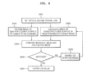
- FIG. 4 is a flowchart for explaining an optical measurement method according to an exemplary embodiment.
- optical scheme parameters for setting a microscope optical system to record an image of a nanostructured surface NS are set (S201).
- the optical scheme parameters may be the parameters described with reference to FIGS. 2 and 3 .
- a defocused image of the nanostructured surface NS is recorded by using a microscope optical system formed according to the optical scheme parameters (S202).
- S202 optical scheme parameters
- the sample 2 having the nanostructured surface NS is arranged at an incline with respect to the objective lens 1.
- the image of the nanostructured surface NS is calculated in consideration of the set optical scheme parameters and the predetermined CD range (S203).
- a software module for calculation is realized owing to a combination of methods of electromagnetic field calculation RCWA [ see reference 5] and FDTD [ see reference 6], which are based on an accurate solution of the Maxwell's equation.
- Input parameters for calculation are optical scheme parameters set to define conditions for illumination and nanostructured surface recording, and a CD value variation range. In an actual semiconductor manufacturing process, an approximate CD value variation range is well known and may be determined according to the opinions of experts.
- the calculated image and the measured image are compared with each other (S204).
- the best estimation of the measured CD value and/or a CD value variation range that is more narrowly adjusted are produced.
- Some exemplary methods for comparing digital images to be applied to the software module for comparison are known.
- a result of the comparison may be a number indicating a degree of matching between the measured image and the calculated image.
- a focus metric parameter [ see reference 7] which is defined to analyze images, each having a different degree of defocus may be used and is described below with reference to FIGS. 5A, 5B , and 6 .
- a degree of matching between a calculated image and a measured image is determined within a given range of accuracy (S205).
- a CD value at which the two images are matched is output as a measured CD value. If the two images do not match, a CD variation range is changed (S206), an image of the nanostructured surface NS is calculated (S203), and a newly calculated image is compared with the measured image (S204).
- a more narrowly adjusted CD value variation range may be determined according to a result of the comparison between the measured image and the calculated image.
- a CD value by comparing the measured image and the calculated image.
- an optimization technique and an image library calculation technology may be used.
- the optimization technique the optimal estimation of a CD value is obtained when an absolute value between the measured image and the calculated image is minimum.
- the library calculation technology is used, the measured image is compared with previously calculated images step-by-step on an assumption that a CD value changes within a known range.
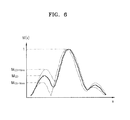
- FIG. 5A is an example of a measurement image of a nanostructured surface of a sample, in which a periodic grating is formed on a glass surface with a period of about 3 ⁇ m and a grating line having a height of about 100 nm.
- FIG. 5B shows a focus metric curve extracted from the image of FIG. 5A .
- a focus metric parameter denotes a characteristic of contrast of an image in a given degree of defocusing and may be a standard deviation calculated from a digital image indicating a data array like the equation below.
- Parameters M(I i,j ) depending on a topology of an object and the degree of defocusing are given corresponding to defocused images I i,j .
- the parameter characterizes image contrast at the given degree of defocusing.
- M(I i,j ) denotes a focus metric
- I i,j denotes a pixel intensity in coordination ( i,j ) in an image
- I denotes an average intensity of all pixels of an image
- N denotes the total number of image pixels.
- a through-focus focus-metric curve M(h) may be obtained by calculating a focus metric of an image at each defocus position.
- h is the position of an object in a focus direction.
- the focus metric curve may be calculated along the investigated inclined surface.
- a predetermined window is defined. The size of a window is small so that a degree of defocusing may be regarded as a constant in the window.
- the window is scanned along the nanostructured surface NS and the focus metric is calculated at each window position.
- a focus metric M(x) is obtained as a result of the image processing, where x denotes a coordinate indicating the position of the window, that is, a coordinate according to a direction in which the nanostructured surface NS is inclined.
- an arrow indicates a surface slope direction. Moire strips are easily identified by an arrow direction on the image and scanning windows are seen at some locations on the image.
- FIG. 5B illustrates a focus metric curve extracted from the image of FIG. 5A , that is, an M(x) graph.
- the shape of the curve and all essential features are dependent on the optical scheme parameters defining conditions for illumination and image recording, and a CD of the grating (having a height of 100 nm).
- FIG. 6 shows three focus metric curves calculated within the range of grating lines height variation CD-10nm ⁇ CD ⁇ CD+10nm, as an example of a library construction of a calculated image for comparison with a measured image.
- the focus metric curves M(x) are normalized to 1 and the shapes of curves calculated with respect to grating having a height difference of 10 nm are similar to one another.
- the curves have three maximum points that are clearly shown.
- the measured and calculated focus metric curves may be compared with a predetermined parameter related to the measured CD.
- the parameter for comparing the focus metric curves extracted from the measurement and the calculation corresponds to the left maximum value of the curves and is a focus metric value satisfying the following condition.
- a CD value may be assumed to be the best estimation of a measured CD* value.
- a single defocused image is measured with respect to a nanostructured surface of a sample to be examined and a CD value is estimated by comparing the estimated defocused image with a calculated image.
- the single defocused image is an image having a different degree of defocusing.
- a CD of a nanostructure having not only a periodic structure but also a non-periodic structure may be measured.
Landscapes
- Physics & Mathematics (AREA)
- General Physics & Mathematics (AREA)
- Engineering & Computer Science (AREA)
- Multimedia (AREA)
- Computer Vision & Pattern Recognition (AREA)
- Chemical & Material Sciences (AREA)
- Analytical Chemistry (AREA)
- Optics & Photonics (AREA)
- Microscoopes, Condenser (AREA)
- Length Measuring Devices By Optical Means (AREA)
Applications Claiming Priority (2)
| Application Number | Priority Date | Filing Date | Title |
|---|---|---|---|
| RU2011142372/28A RU2481555C1 (ru) | 2011-10-20 | 2011-10-20 | Оптическая измерительная система и способ измерения критического размера наноструктур на плоской поверхности |
| KR1020120085388A KR101928439B1 (ko) | 2011-10-20 | 2012-08-03 | 나노구조의 cd에 대한 광학 측정 시스템 및 측정 방법 |
Publications (3)
| Publication Number | Publication Date |
|---|---|
| EP2587313A2 true EP2587313A2 (de) | 2013-05-01 |
| EP2587313A3 EP2587313A3 (de) | 2015-01-14 |
| EP2587313B1 EP2587313B1 (de) | 2016-05-11 |
Family
ID=47471462
Family Applications (1)
| Application Number | Title | Priority Date | Filing Date |
|---|---|---|---|
| EP12189262.4A Active EP2587313B1 (de) | 2011-10-20 | 2012-10-19 | Optikmesssystem und Verfahren zum Messen kritischer Abmessungen von Nanostrukturen |
Country Status (2)
| Country | Link |
|---|---|
| US (1) | US9360662B2 (de) |
| EP (1) | EP2587313B1 (de) |
Cited By (2)
| Publication number | Priority date | Publication date | Assignee | Title |
|---|---|---|---|---|
| CZ304851B6 (cs) * | 2013-11-21 | 2014-12-03 | ÄŚeskĂ© vysokĂ© uÄŤenĂ technickĂ© v Praze - fakulta stavebnĂ | Zařízení pro měření rozlišovací schopnosti mikroskopových objektivů |
| US9995648B2 (en) | 2014-11-10 | 2018-06-12 | Samsung Electronics Co., Ltd. | Optical measurement system and method for measuring critical dimension of nanostructure |
Families Citing this family (9)
| Publication number | Priority date | Publication date | Assignee | Title |
|---|---|---|---|---|
| WO2015080480A1 (ko) * | 2013-11-29 | 2015-06-04 | (주)넥스틴 | 웨이퍼 영상 검사 장치 |
| RU2560245C1 (ru) * | 2014-03-26 | 2015-08-20 | Самсунг Электроникс Ко., Лтд. | Способ мультиспектральной визуализации и устройство для измерения критического размера наноструктур |
| US9400254B2 (en) | 2014-03-26 | 2016-07-26 | Samsung Electronics Co., Ltd. | Method and device for measuring critical dimension of nanostructure |
| US10983440B2 (en) * | 2016-05-23 | 2021-04-20 | Asml Netherlands B.V. | Selection of substrate measurement recipes |
| US10731979B2 (en) | 2018-01-12 | 2020-08-04 | Applied Materials Israel Ltd. | Method for monitoring nanometric structures |
| KR102674578B1 (ko) * | 2019-08-06 | 2024-06-12 | 삼성디스플레이 주식회사 | 포토 레지스트 패턴의 임계 치수 검사 방법 |
| KR102825815B1 (ko) * | 2020-06-18 | 2025-06-27 | 삼성전자주식회사 | 스루-포커스 이미지 기반 계측 장치, 그것의 동작 방법, 및 그 동작을 실행하는 컴퓨팅 장치 |
| CN113420260B (zh) * | 2021-07-01 | 2022-10-28 | 深圳市埃芯半导体科技有限公司 | 一种半导体尺寸的测量计算方法、装置及计算机存储介质 |
| CN120609551B (zh) * | 2025-08-12 | 2025-10-31 | 苏州矽行半导体技术有限公司 | 一种明场显微成像像质检测系统 |
Family Cites Families (25)
| Publication number | Priority date | Publication date | Assignee | Title |
|---|---|---|---|---|
| US6774991B1 (en) | 1999-05-27 | 2004-08-10 | Inspex Incorporated | Method and apparatus for inspecting a patterned semiconductor wafer |
| JP3691404B2 (ja) | 2001-02-28 | 2005-09-07 | 株式会社日立国際電気 | 微小寸法測定装置 |
| US6586160B2 (en) | 2001-03-26 | 2003-07-01 | Motorola, Inc. | Method for patterning resist |
| US7037659B2 (en) * | 2002-01-31 | 2006-05-02 | Nimblegen Systems Inc. | Apparatus for constructing DNA probes having a prismatic and kaleidoscopic light homogenizer |
| US6992765B2 (en) * | 2002-10-11 | 2006-01-31 | Intralase Corp. | Method and system for determining the alignment of a surface of a material in relation to a laser beam |
| US6934929B2 (en) | 2003-01-13 | 2005-08-23 | Lsi Logic Corporation | Method for improving OPC modeling |
| JP4254469B2 (ja) * | 2003-05-23 | 2009-04-15 | 日本ビクター株式会社 | 光ピックアップ装置及び光記録媒体駆動装置 |
| US7061623B2 (en) | 2003-08-25 | 2006-06-13 | Spectel Research Corporation | Interferometric back focal plane scatterometry with Koehler illumination |
| KR100574963B1 (ko) | 2003-12-29 | 2006-04-28 | 삼성전자주식회사 | 파장가변 레이저 장치를 구비한 광학적 임계치수 측정장치및 그 측정장치를 이용한 임계치수 측정방법 |
| JP4166166B2 (ja) * | 2004-02-02 | 2008-10-15 | 株式会社東芝 | 露光投影像予測システム及び露光投影像予測方法 |
| US7642019B2 (en) | 2005-04-15 | 2010-01-05 | Samsung Electronics Co., Ltd. | Methods for monitoring and adjusting focus variation in a photolithographic process using test features printed from photomask test pattern images; and machine readable program storage device having instructions therefore |
| WO2007095090A2 (en) | 2006-02-10 | 2007-08-23 | Monogen, Inc. | Method and apparatus and computer program product for collecting digital image data from microscope media-based specimens |
| TWI292031B (en) * | 2006-02-10 | 2008-01-01 | Ind Tech Res Inst | Dimension measuring method and optical measuring system implemented with the method |
| WO2007124930A1 (en) * | 2006-04-28 | 2007-11-08 | Micronic Laser Systems Ab | Method and apparatus for recording of images and study of surfaces |
| KR20080051554A (ko) | 2006-12-06 | 2008-06-11 | 삼성전자주식회사 | 반도체 장치의 임계 선폭 평가 방법 |
| US7864294B2 (en) | 2007-05-29 | 2011-01-04 | Micron Technology, Inc. | Focus sensitive lithographic apparatus, systems, and methods |
| TWI378221B (en) | 2007-09-21 | 2012-12-01 | Ind Tech Res Inst | Scatterfield microscopical measuring method and apparatus |
| US7812943B2 (en) | 2007-10-29 | 2010-10-12 | The United States Of America As Represented By The Secretary Of Commerce | Zeroeth order imaging |
| TW200928598A (en) | 2007-12-24 | 2009-07-01 | Ind Tech Res Inst | Inclined exposure lithography system |
| US8319971B2 (en) | 2008-05-06 | 2012-11-27 | Industrial Technology Research Institute | Scatterfield microscopical measuring method and apparatus |
| EP2246725A3 (de) * | 2009-04-30 | 2011-01-26 | Olympus Corporation | Mikroskop mit unbeweglicher Bildgebungseinrichtung und beweglichem Objektiv |
| CA2763826C (en) * | 2009-06-17 | 2020-04-07 | 3Shape A/S | Focus scanning apparatus |
| NL2005521A (en) * | 2009-10-22 | 2011-04-26 | Asml Netherlands Bv | Methods and apparatus for calculating electromagnetic scattering properties of a structure using a normal-vector field and for reconstruction of approximate structures. |
| US8913121B2 (en) * | 2010-07-11 | 2014-12-16 | Spynsite, LLC | System for image rendering or spectral recognition |
| JP5854680B2 (ja) * | 2011-07-25 | 2016-02-09 | キヤノン株式会社 | 撮像装置 |
-
2012
- 2012-10-19 EP EP12189262.4A patent/EP2587313B1/de active Active
- 2012-10-19 US US13/656,180 patent/US9360662B2/en active Active
Non-Patent Citations (8)
| Title |
|---|
| "Encyclopedia of physics and engineering. Microscopy" |
| ATTOTA, R.; SILVER R. M.; POTZICK, J.: "Optical illumination and critical dimension analysis using the through-focus focus metric", PROC. SPIE, 6289, 2006 |
| ATTOTA, R.; SILVER, R. M.; BARNES, B. M.: "Optical through-focus technique that differentiates small changes in line width, line height, and sidewall angle for CD, overlay, and defect metrology applications", PROC. SPIE 6922, 2008 |
| HARLAND G. TOMPKINS; EUGENE A. IRENE: "Handbook of ellipsometry" |
| K. UMASHANKAR; A. TAFLOVE: "A Novel Method to Analyze Electromagnetic Scattering of Complex Objects", IEEE, 1982 |
| M. G. MOHARAM; DREW A. POMMET; ERIC B. GRANN, J. OPT. SOC. AM. A, vol. 12, no. 5, May 1995 (1995-05-01), pages 1077 - 1086 |
| PETRE CATALIN LOGOFATU, ROM. JOURN. PHYS., vol. 55, no. 3-4, 2010, pages 376 - 385 |
| RAY J. HOOBLER; EBRU APAK, PROCEEDINGS OF SPIE VOL. 5256 23RD ANNUAL BACUS SYMPOSIUM ON PHOTOMASK TECHNOLOGY, vol. 5256 |
Cited By (2)
| Publication number | Priority date | Publication date | Assignee | Title |
|---|---|---|---|---|
| CZ304851B6 (cs) * | 2013-11-21 | 2014-12-03 | ÄŚeskĂ© vysokĂ© uÄŤenĂ technickĂ© v Praze - fakulta stavebnĂ | Zařízení pro měření rozlišovací schopnosti mikroskopových objektivů |
| US9995648B2 (en) | 2014-11-10 | 2018-06-12 | Samsung Electronics Co., Ltd. | Optical measurement system and method for measuring critical dimension of nanostructure |
Also Published As
| Publication number | Publication date |
|---|---|
| EP2587313B1 (de) | 2016-05-11 |
| US20130107030A1 (en) | 2013-05-02 |
| US9360662B2 (en) | 2016-06-07 |
| EP2587313A3 (de) | 2015-01-14 |
Similar Documents
| Publication | Publication Date | Title |
|---|---|---|
| EP2587313B1 (de) | Optikmesssystem und Verfahren zum Messen kritischer Abmessungen von Nanostrukturen | |
| US10697900B2 (en) | Correlating SEM and optical images for wafer noise nuisance identification | |
| TWI677679B (zh) | 在雷射暗場系統中用於斑點抑制之方法及裝置 | |
| US6317211B1 (en) | Optical metrology tool and method of using same | |
| TWI821586B (zh) | 用於在計量量測中減少錯誤之系統及方法 | |
| JP6758309B2 (ja) | フォーカスエラー感応性が減少した光学的計測 | |
| US9222897B2 (en) | Method for characterizing a feature on a mask and device for carrying out the method | |
| CN111819596B (zh) | 组合模拟及光学显微术以确定检验模式的方法和系统 | |
| US8045179B1 (en) | Bright and dark field scatterometry systems for line roughness metrology | |
| KR20190082911A (ko) | 3차원 반도체 구조체들의 검사를 위한 결함 발견 및 레시피 최적화 | |
| CN107924561A (zh) | 使用图像的以模型为基础的计量 | |
| WO2007112300A2 (en) | Systems and methods for measuring one or more characteristics of patterned features on a specimen | |
| KR101919901B1 (ko) | 웨이퍼 검사 방법 | |
| JP4359689B2 (ja) | 検査装置及び検査方法、パターン基板の製造方法 | |
| JPH0926396A (ja) | 異物等の欠陥検査方法及びその装置 | |
| KR102026742B1 (ko) | 광학 측정 시스템 및 임계치수를 측정하는 방법 | |
| JP4325909B2 (ja) | 欠陥検査装置、欠陥検査方法、光学式走査装置、半導体デバイス製造方法 | |
| KR101928439B1 (ko) | 나노구조의 cd에 대한 광학 측정 시스템 및 측정 방법 | |
| US9523645B2 (en) | Lenticular wafer inspection | |
| JP2712362B2 (ja) | レジストパターンの検査装置 | |
| KR20260032899A (ko) | Cmos 언더 어레이(cua) 구조가 존재하는 경우 cua 구조의 분류와 유효 매질 모델을 사용한 계측 | |
| CN116368377B (zh) | 多视角晶片分析 | |
| JP5046054B2 (ja) | 欠陥検査装置、欠陥検査方法、光学式走査装置、半導体デバイス製造方法 | |
| US20230205095A1 (en) | Method and system for determining one or more dimensions of one or more structures on a sample surface | |
| CN103307997A (zh) | 一种角分辨散射测量装置及其测量方法 |
Legal Events
| Date | Code | Title | Description |
|---|---|---|---|
| PUAI | Public reference made under article 153(3) epc to a published international application that has entered the european phase |
Free format text: ORIGINAL CODE: 0009012 |
|
| AK | Designated contracting states |
Kind code of ref document: A2 Designated state(s): AL AT BE BG CH CY CZ DE DK EE ES FI FR GB GR HR HU IE IS IT LI LT LU LV MC MK MT NL NO PL PT RO RS SE SI SK SM TR |
|
| AX | Request for extension of the european patent |
Extension state: BA ME |
|
| PUAL | Search report despatched |
Free format text: ORIGINAL CODE: 0009013 |
|
| AK | Designated contracting states |
Kind code of ref document: A3 Designated state(s): AL AT BE BG CH CY CZ DE DK EE ES FI FR GB GR HR HU IE IS IT LI LT LU LV MC MK MT NL NO PL PT RO RS SE SI SK SM TR |
|
| AX | Request for extension of the european patent |
Extension state: BA ME |
|
| RIC1 | Information provided on ipc code assigned before grant |
Ipc: G03F 7/20 20060101AFI20141205BHEP |
|
| 17P | Request for examination filed |
Effective date: 20150714 |
|
| RBV | Designated contracting states (corrected) |
Designated state(s): AL AT BE BG CH CY CZ DE DK EE ES FI FR GB GR HR HU IE IS IT LI LT LU LV MC MK MT NL NO PL PT RO RS SE SI SK SM TR |
|
| GRAP | Despatch of communication of intention to grant a patent |
Free format text: ORIGINAL CODE: EPIDOSNIGR1 |
|
| INTG | Intention to grant announced |
Effective date: 20151112 |
|
| GRAS | Grant fee paid |
Free format text: ORIGINAL CODE: EPIDOSNIGR3 |
|
| GRAA | (expected) grant |
Free format text: ORIGINAL CODE: 0009210 |
|
| AK | Designated contracting states |
Kind code of ref document: B1 Designated state(s): AL AT BE BG CH CY CZ DE DK EE ES FI FR GB GR HR HU IE IS IT LI LT LU LV MC MK MT NL NO PL PT RO RS SE SI SK SM TR |
|
| REG | Reference to a national code |
Ref country code: GB Ref legal event code: FG4D |
|
| REG | Reference to a national code |
Ref country code: CH Ref legal event code: EP |
|
| REG | Reference to a national code |
Ref country code: AT Ref legal event code: REF Ref document number: 799121 Country of ref document: AT Kind code of ref document: T Effective date: 20160515 |
|
| REG | Reference to a national code |
Ref country code: IE Ref legal event code: FG4D |
|
| REG | Reference to a national code |
Ref country code: DE Ref legal event code: R096 Ref document number: 602012018300 Country of ref document: DE |
|
| REG | Reference to a national code |
Ref country code: LT Ref legal event code: MG4D |
|
| REG | Reference to a national code |
Ref country code: NL Ref legal event code: MP Effective date: 20160511 |
|
| REG | Reference to a national code |
Ref country code: FR Ref legal event code: PLFP Year of fee payment: 5 |
|
| PG25 | Lapsed in a contracting state [announced via postgrant information from national office to epo] |
Ref country code: NL Free format text: LAPSE BECAUSE OF FAILURE TO SUBMIT A TRANSLATION OF THE DESCRIPTION OR TO PAY THE FEE WITHIN THE PRESCRIBED TIME-LIMIT Effective date: 20160511 Ref country code: NO Free format text: LAPSE BECAUSE OF FAILURE TO SUBMIT A TRANSLATION OF THE DESCRIPTION OR TO PAY THE FEE WITHIN THE PRESCRIBED TIME-LIMIT Effective date: 20160811 Ref country code: LT Free format text: LAPSE BECAUSE OF FAILURE TO SUBMIT A TRANSLATION OF THE DESCRIPTION OR TO PAY THE FEE WITHIN THE PRESCRIBED TIME-LIMIT Effective date: 20160511 Ref country code: FI Free format text: LAPSE BECAUSE OF FAILURE TO SUBMIT A TRANSLATION OF THE DESCRIPTION OR TO PAY THE FEE WITHIN THE PRESCRIBED TIME-LIMIT Effective date: 20160511 |
|
| REG | Reference to a national code |
Ref country code: AT Ref legal event code: MK05 Ref document number: 799121 Country of ref document: AT Kind code of ref document: T Effective date: 20160511 |
|
| PG25 | Lapsed in a contracting state [announced via postgrant information from national office to epo] |
Ref country code: SE Free format text: LAPSE BECAUSE OF FAILURE TO SUBMIT A TRANSLATION OF THE DESCRIPTION OR TO PAY THE FEE WITHIN THE PRESCRIBED TIME-LIMIT Effective date: 20160511 Ref country code: LV Free format text: LAPSE BECAUSE OF FAILURE TO SUBMIT A TRANSLATION OF THE DESCRIPTION OR TO PAY THE FEE WITHIN THE PRESCRIBED TIME-LIMIT Effective date: 20160511 Ref country code: ES Free format text: LAPSE BECAUSE OF FAILURE TO SUBMIT A TRANSLATION OF THE DESCRIPTION OR TO PAY THE FEE WITHIN THE PRESCRIBED TIME-LIMIT Effective date: 20160511 Ref country code: HR Free format text: LAPSE BECAUSE OF FAILURE TO SUBMIT A TRANSLATION OF THE DESCRIPTION OR TO PAY THE FEE WITHIN THE PRESCRIBED TIME-LIMIT Effective date: 20160511 Ref country code: RS Free format text: LAPSE BECAUSE OF FAILURE TO SUBMIT A TRANSLATION OF THE DESCRIPTION OR TO PAY THE FEE WITHIN THE PRESCRIBED TIME-LIMIT Effective date: 20160511 Ref country code: PT Free format text: LAPSE BECAUSE OF FAILURE TO SUBMIT A TRANSLATION OF THE DESCRIPTION OR TO PAY THE FEE WITHIN THE PRESCRIBED TIME-LIMIT Effective date: 20160912 Ref country code: GR Free format text: LAPSE BECAUSE OF FAILURE TO SUBMIT A TRANSLATION OF THE DESCRIPTION OR TO PAY THE FEE WITHIN THE PRESCRIBED TIME-LIMIT Effective date: 20160812 |
|
| PG25 | Lapsed in a contracting state [announced via postgrant information from national office to epo] |
Ref country code: IT Free format text: LAPSE BECAUSE OF FAILURE TO SUBMIT A TRANSLATION OF THE DESCRIPTION OR TO PAY THE FEE WITHIN THE PRESCRIBED TIME-LIMIT Effective date: 20160511 |
|
| PG25 | Lapsed in a contracting state [announced via postgrant information from national office to epo] |
Ref country code: RO Free format text: LAPSE BECAUSE OF FAILURE TO SUBMIT A TRANSLATION OF THE DESCRIPTION OR TO PAY THE FEE WITHIN THE PRESCRIBED TIME-LIMIT Effective date: 20160511 Ref country code: CZ Free format text: LAPSE BECAUSE OF FAILURE TO SUBMIT A TRANSLATION OF THE DESCRIPTION OR TO PAY THE FEE WITHIN THE PRESCRIBED TIME-LIMIT Effective date: 20160511 Ref country code: EE Free format text: LAPSE BECAUSE OF FAILURE TO SUBMIT A TRANSLATION OF THE DESCRIPTION OR TO PAY THE FEE WITHIN THE PRESCRIBED TIME-LIMIT Effective date: 20160511 Ref country code: SK Free format text: LAPSE BECAUSE OF FAILURE TO SUBMIT A TRANSLATION OF THE DESCRIPTION OR TO PAY THE FEE WITHIN THE PRESCRIBED TIME-LIMIT Effective date: 20160511 Ref country code: DK Free format text: LAPSE BECAUSE OF FAILURE TO SUBMIT A TRANSLATION OF THE DESCRIPTION OR TO PAY THE FEE WITHIN THE PRESCRIBED TIME-LIMIT Effective date: 20160511 |
|
| REG | Reference to a national code |
Ref country code: DE Ref legal event code: R097 Ref document number: 602012018300 Country of ref document: DE |
|
| PG25 | Lapsed in a contracting state [announced via postgrant information from national office to epo] |
Ref country code: AT Free format text: LAPSE BECAUSE OF FAILURE TO SUBMIT A TRANSLATION OF THE DESCRIPTION OR TO PAY THE FEE WITHIN THE PRESCRIBED TIME-LIMIT Effective date: 20160511 Ref country code: SM Free format text: LAPSE BECAUSE OF FAILURE TO SUBMIT A TRANSLATION OF THE DESCRIPTION OR TO PAY THE FEE WITHIN THE PRESCRIBED TIME-LIMIT Effective date: 20160511 Ref country code: PL Free format text: LAPSE BECAUSE OF FAILURE TO SUBMIT A TRANSLATION OF THE DESCRIPTION OR TO PAY THE FEE WITHIN THE PRESCRIBED TIME-LIMIT Effective date: 20160511 Ref country code: BE Free format text: LAPSE BECAUSE OF FAILURE TO SUBMIT A TRANSLATION OF THE DESCRIPTION OR TO PAY THE FEE WITHIN THE PRESCRIBED TIME-LIMIT Effective date: 20160511 |
|
| PLBE | No opposition filed within time limit |
Free format text: ORIGINAL CODE: 0009261 |
|
| STAA | Information on the status of an ep patent application or granted ep patent |
Free format text: STATUS: NO OPPOSITION FILED WITHIN TIME LIMIT |
|
| 26N | No opposition filed |
Effective date: 20170214 |
|
| PG25 | Lapsed in a contracting state [announced via postgrant information from national office to epo] |
Ref country code: SI Free format text: LAPSE BECAUSE OF FAILURE TO SUBMIT A TRANSLATION OF THE DESCRIPTION OR TO PAY THE FEE WITHIN THE PRESCRIBED TIME-LIMIT Effective date: 20160511 |
|
| REG | Reference to a national code |
Ref country code: CH Ref legal event code: PL |
|
| PG25 | Lapsed in a contracting state [announced via postgrant information from national office to epo] |
Ref country code: MC Free format text: LAPSE BECAUSE OF FAILURE TO SUBMIT A TRANSLATION OF THE DESCRIPTION OR TO PAY THE FEE WITHIN THE PRESCRIBED TIME-LIMIT Effective date: 20160511 |
|
| REG | Reference to a national code |
Ref country code: IE Ref legal event code: MM4A |
|
| PG25 | Lapsed in a contracting state [announced via postgrant information from national office to epo] |
Ref country code: CH Free format text: LAPSE BECAUSE OF NON-PAYMENT OF DUE FEES Effective date: 20161031 Ref country code: LI Free format text: LAPSE BECAUSE OF NON-PAYMENT OF DUE FEES Effective date: 20161031 |
|
| PG25 | Lapsed in a contracting state [announced via postgrant information from national office to epo] |
Ref country code: LU Free format text: LAPSE BECAUSE OF NON-PAYMENT OF DUE FEES Effective date: 20161019 |
|
| REG | Reference to a national code |
Ref country code: FR Ref legal event code: PLFP Year of fee payment: 6 |
|
| PG25 | Lapsed in a contracting state [announced via postgrant information from national office to epo] |
Ref country code: IE Free format text: LAPSE BECAUSE OF NON-PAYMENT OF DUE FEES Effective date: 20161019 |
|
| PG25 | Lapsed in a contracting state [announced via postgrant information from national office to epo] |
Ref country code: HU Free format text: LAPSE BECAUSE OF FAILURE TO SUBMIT A TRANSLATION OF THE DESCRIPTION OR TO PAY THE FEE WITHIN THE PRESCRIBED TIME-LIMIT; INVALID AB INITIO Effective date: 20121019 Ref country code: CY Free format text: LAPSE BECAUSE OF FAILURE TO SUBMIT A TRANSLATION OF THE DESCRIPTION OR TO PAY THE FEE WITHIN THE PRESCRIBED TIME-LIMIT Effective date: 20160511 |
|
| PG25 | Lapsed in a contracting state [announced via postgrant information from national office to epo] |
Ref country code: MK Free format text: LAPSE BECAUSE OF FAILURE TO SUBMIT A TRANSLATION OF THE DESCRIPTION OR TO PAY THE FEE WITHIN THE PRESCRIBED TIME-LIMIT Effective date: 20160511 Ref country code: MT Free format text: LAPSE BECAUSE OF NON-PAYMENT OF DUE FEES Effective date: 20161031 Ref country code: TR Free format text: LAPSE BECAUSE OF FAILURE TO SUBMIT A TRANSLATION OF THE DESCRIPTION OR TO PAY THE FEE WITHIN THE PRESCRIBED TIME-LIMIT Effective date: 20160511 Ref country code: IS Free format text: LAPSE BECAUSE OF FAILURE TO SUBMIT A TRANSLATION OF THE DESCRIPTION OR TO PAY THE FEE WITHIN THE PRESCRIBED TIME-LIMIT Effective date: 20160511 |
|
| PG25 | Lapsed in a contracting state [announced via postgrant information from national office to epo] |
Ref country code: BG Free format text: LAPSE BECAUSE OF FAILURE TO SUBMIT A TRANSLATION OF THE DESCRIPTION OR TO PAY THE FEE WITHIN THE PRESCRIBED TIME-LIMIT Effective date: 20160511 |
|
| REG | Reference to a national code |
Ref country code: FR Ref legal event code: PLFP Year of fee payment: 7 |
|
| PG25 | Lapsed in a contracting state [announced via postgrant information from national office to epo] |
Ref country code: AL Free format text: LAPSE BECAUSE OF FAILURE TO SUBMIT A TRANSLATION OF THE DESCRIPTION OR TO PAY THE FEE WITHIN THE PRESCRIBED TIME-LIMIT Effective date: 20160511 |
|
| P01 | Opt-out of the competence of the unified patent court (upc) registered |
Effective date: 20230530 |
|
| PGFP | Annual fee paid to national office [announced via postgrant information from national office to epo] |
Ref country code: GB Payment date: 20250911 Year of fee payment: 14 |
|
| PGFP | Annual fee paid to national office [announced via postgrant information from national office to epo] |
Ref country code: FR Payment date: 20250908 Year of fee payment: 14 |
|
| PGFP | Annual fee paid to national office [announced via postgrant information from national office to epo] |
Ref country code: DE Payment date: 20250910 Year of fee payment: 14 |