EP2590159A1 - Appareil d'affichage, appareil d'affichage à cristaux liquides et récepteur de télévision - Google Patents
Appareil d'affichage, appareil d'affichage à cristaux liquides et récepteur de télévision Download PDFInfo
- Publication number
- EP2590159A1 EP2590159A1 EP11800513.1A EP11800513A EP2590159A1 EP 2590159 A1 EP2590159 A1 EP 2590159A1 EP 11800513 A EP11800513 A EP 11800513A EP 2590159 A1 EP2590159 A1 EP 2590159A1
- Authority
- EP
- European Patent Office
- Prior art keywords
- data signal
- pixel electrode
- pixels
- pixel
- signal line
- Prior art date
- Legal status (The legal status is an assumption and is not a legal conclusion. Google has not performed a legal analysis and makes no representation as to the accuracy of the status listed.)
- Granted
Links
Images












Classifications
-
- G—PHYSICS
- G09—EDUCATION; CRYPTOGRAPHY; DISPLAY; ADVERTISING; SEALS
- G09G—ARRANGEMENTS OR CIRCUITS FOR CONTROL OF INDICATING DEVICES USING STATIC MEANS TO PRESENT VARIABLE INFORMATION
- G09G3/00—Control arrangements or circuits, of interest only in connection with visual indicators other than cathode-ray tubes
- G09G3/20—Control arrangements or circuits, of interest only in connection with visual indicators other than cathode-ray tubes for presentation of an assembly of a number of characters, e.g. a page, by composing the assembly by combination of individual elements arranged in a matrix no fixed position being assigned to or needed to be assigned to the individual characters or partial characters
- G09G3/34—Control arrangements or circuits, of interest only in connection with visual indicators other than cathode-ray tubes for presentation of an assembly of a number of characters, e.g. a page, by composing the assembly by combination of individual elements arranged in a matrix no fixed position being assigned to or needed to be assigned to the individual characters or partial characters by control of light from an independent source
- G09G3/36—Control arrangements or circuits, of interest only in connection with visual indicators other than cathode-ray tubes for presentation of an assembly of a number of characters, e.g. a page, by composing the assembly by combination of individual elements arranged in a matrix no fixed position being assigned to or needed to be assigned to the individual characters or partial characters by control of light from an independent source using liquid crystals
- G09G3/3611—Control of matrices with row and column drivers
- G09G3/3648—Control of matrices with row and column drivers using an active matrix
-
- G—PHYSICS
- G09—EDUCATION; CRYPTOGRAPHY; DISPLAY; ADVERTISING; SEALS
- G09G—ARRANGEMENTS OR CIRCUITS FOR CONTROL OF INDICATING DEVICES USING STATIC MEANS TO PRESENT VARIABLE INFORMATION
- G09G2300/00—Aspects of the constitution of display devices
- G09G2300/04—Structural and physical details of display devices
- G09G2300/0421—Structural details of the set of electrodes
- G09G2300/0426—Layout of electrodes and connections
-
- G—PHYSICS
- G09—EDUCATION; CRYPTOGRAPHY; DISPLAY; ADVERTISING; SEALS
- G09G—ARRANGEMENTS OR CIRCUITS FOR CONTROL OF INDICATING DEVICES USING STATIC MEANS TO PRESENT VARIABLE INFORMATION
- G09G2300/00—Aspects of the constitution of display devices
- G09G2300/04—Structural and physical details of display devices
- G09G2300/0439—Pixel structures
- G09G2300/0443—Pixel structures with several sub-pixels for the same colour in a pixel, not specifically used to display gradations
-
- G—PHYSICS
- G09—EDUCATION; CRYPTOGRAPHY; DISPLAY; ADVERTISING; SEALS
- G09G—ARRANGEMENTS OR CIRCUITS FOR CONTROL OF INDICATING DEVICES USING STATIC MEANS TO PRESENT VARIABLE INFORMATION
- G09G2310/00—Command of the display device
- G09G2310/02—Addressing, scanning or driving the display screen or processing steps related thereto
- G09G2310/0202—Addressing of scan or signal lines
- G09G2310/0205—Simultaneous scanning of several lines in flat panels
-
- G—PHYSICS
- G09—EDUCATION; CRYPTOGRAPHY; DISPLAY; ADVERTISING; SEALS
- G09G—ARRANGEMENTS OR CIRCUITS FOR CONTROL OF INDICATING DEVICES USING STATIC MEANS TO PRESENT VARIABLE INFORMATION
- G09G2320/00—Control of display operating conditions
- G09G2320/02—Improving the quality of display appearance
- G09G2320/0209—Crosstalk reduction, i.e. to reduce direct or indirect influences of signals directed to a certain pixel of the displayed image on other pixels of said image, inclusive of influences affecting pixels in different frames or fields or sub-images which constitute a same image, e.g. left and right images of a stereoscopic display
-
- G—PHYSICS
- G09—EDUCATION; CRYPTOGRAPHY; DISPLAY; ADVERTISING; SEALS
- G09G—ARRANGEMENTS OR CIRCUITS FOR CONTROL OF INDICATING DEVICES USING STATIC MEANS TO PRESENT VARIABLE INFORMATION
- G09G2320/00—Control of display operating conditions
- G09G2320/02—Improving the quality of display appearance
- G09G2320/0233—Improving the luminance or brightness uniformity across the screen
Definitions
- each column of pixels with a plurality of data signal lines generates display unevenness a possible cause of which is a parasitic capacitance between a pixel electrode contained in the column of pixels and a data signal line corresponding to the pixel electrode.
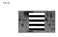
- display unevenness is explained below with reference to Figs. 30 through 35 .
- Fig. 30 shows an example of a display (stripe pattern of black and white lines surrounded by gray) image that is supposed to be displayed.
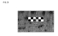
- the letters a to f and A to F each correspond to a single pixel. That is, the pixels a, b, e, f, A, B, E, and F display gray, the pixels c and C display white, and the pixels d and D display black.
- Fig. 32 is an equivalent circuit diagram showing part of a configuration of a conventional liquid crystal panel.
- the pixels 101 to 106 correspond to the pixels a to f of Fig. 31 , respectively
- the pixels 111 to 116 correspond to the pixels A to F of Fig. 31 , respectively.
- the liquid crystal panel 10 thus configured has a retention capacitance ChA formed between the retention capacitor wire 18a and the pixel electrode 17A, a retention capacitance ChB formed between the retention capacitor wire 18b and the pixel electrode 17B, a retention capacitance ChC formed between the retention capacitor wire 18c and the pixel electrode 17C, a retention capacitance ChD formed between the retention capacitor wire 18d and the pixel electrode 17D, a retention capacitance ChE formed between the retention capacitor wire 18e and the pixel electrode 17E, and a retention capacitance ChF formed between the retention capacitor wire 18f and the pixel electrode 17F.
- ChA formed between the retention capacitor wire 18a and the pixel electrode 17A
- a retention capacitance ChB formed between the retention capacitor wire 18b and the pixel electrode 17B
- a retention capacitance ChC formed between the retention capacitor wire 18c and the pixel electrode 17C
- a retention capacitance ChD formed between the retention capacitor wire 18d and the pixel electrode 17D
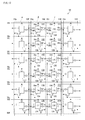
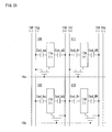
- Fig. 1 shows that the pixel 101 has a capacitance CaP formed between the pixel electrode 17a and the data signal line 15P and a capacitance Car formed between the pixel electrode 17a and the data signal line 15r, that the pixel 102 has a capacitance CbP formed between the pixel electrode 17b and the data signal line 15P and a capacitance Cbr formed between the pixel electrode 17b and the data signal line 15r, that the pixel 103 has a capacitance CcP formed between the pixel electrode 17c and the data signal line 15P and a capacitance Ccr formed between the pixel electrode 17c and the data signal line 15r, that the pixel 104 has a capacitance CdP formed between the pixel electrode 17d and the data signal line 15P and a capacitance Cdr formed between the pixel electrode 17d and the data signal line 15r, that the pixel 105 has a capacitance CeP formed between the pixel electrode 17e and the data signal line 15P and
- the pixel 111 has a capacitance CAQ formed between the pixel electrode 17A and the data signal line 15Q and a capacitance CAs formed between the pixel electrode 17A and the data signal line 15s.
- the pixel 112 has a capacitance CBQ formed between the pixel electrode 17B and the data signal line 15Q and a capacitance CBs formed between the pixel electrode 17B and the data signal line 15s.
- the pixel 113 has a capacitance CCQ formed between the pixel electrode 17C and the data signal line 15Q and a capacitance CCs formed between the pixel electrode 17C and the data signal line 15s.
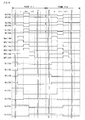
- the potentials of the data signals that are supplied to the data signal lines 15q and 15Q change in a falling direction (negative direction)
- the potentials of the data signals that are supplied to the data signal lines 15q and 15Q change in a rising direction (positive direction).
- the pixel potential Vb (data signal of a positive polarity corresponding to gray) written during the kth horizontal scanning period changes in a falling direction (negative direction) due to the parasitic capacitances Csd_bq and Csd_bQ between the pixel electrode 17b and the data signal lines 15q and 15Q, respectively (see Fig.
- a data signal of a negative polarity, a data signal of a positive polarity, a data signal of a negative polarity, a data signal of a positive polarity, a data signal of a negative polarity, and a data signal of a positive polarity are written to the pixel electrode 17a of the pixel 101, the pixel electrode 17b of the pixel 102, the pixel electrode 17c of the pixel 103, the pixel electrode 17d of the pixel 104, the pixel electrode 17e of the pixel 105, and the pixel electrode 17f of the pixel 106, respectively.
- Fig. 11 is a plan view showing Example Configuration 2 of the liquid crystal panel 20 of Fig. 7 .
- the present liquid crystal panel 20 has its transistor 12a provided near an intersection between the data signal line 15Q and the scanning signal line 16a, has its transistor 12b provided near an intersection between the data signal line 15q and the scanning signal line 16b, has its transistor 12A provided near an intersection between the data signal line 15r and the scanning signal line 16a, and has its transistor 12B provided near an intersection between the data signal line 15R and the scanning signal line 16b.
- the other components of the liquid crystal panel 20 of Fig. 7 are identical to those of the liquid crystal panel 10 of Fig. 5 .
- the scanning signal line 16ab functions as the gate electrode of the transistor 12a, which has its source electrode connected to the data signal line 15q and which has its drain electrode connected to a capacitor electrode 37a via a drain drawing electrode 27a.
- the capacitor electrode 37a is provided above the retention capacitor wire 18g and is connected to the pixel electrode 17a via a contact hole 11a.
- the scanning signal line 16ab functions as the gate electrode of the transistor 12b, which has its source electrode connected to the data signal line 15Q and which has its drain electrode connected to a capacitor electrode 37b via a drain drawing electrode 27b.
- the capacitor electrode 37b is provided above the retention capacitor wire 18h and is connected to the pixel electrode 17b via a contact hole 11b.
- the pixel 111 has its pixel electrode 17Am connected to the data signal line 15r via a transistor 12Am connected to the scanning signal line 16a, and has its pixel electrode 17 As connected to the data signal line 15r via a transistor 12As connected to the scanning signal line 16a.
- the pixel 112 has its pixel electrode 17Bm connected to the data signal line 15R via a transistor 12Bm connected to the scanning signal line 16b, and has its pixel electrode 17Bs connected to the data signal line 15R via a transistor 12Bs connected to the scanning signal line 16b.
- the display control circuit generates a data start pulse signal SSP, a data clock signal SCK, a charge share signal sh, a digital image signal DA (which is a signal corresponding to the video signal Dv), a gate start pulse signal GSP, a gate clock signal GCK, and a gate driver output control signal (scanning signal output control signal) GOE in accordance with the signals Dv, HSY, VSY, and Dc thus received, and then outputs the signals SSP, SCK, sh, DA, GSP, GCK, and GOE.
- the signals SSP, SCK, sh, DA, GSP, GCK, and GOE serve as signals for causing the display section to display the image represented by the digital video signal Dv.
- the digital image signal DA represents the image to be displayed.
- the present liquid crystal display apparatus can also be applied to a digital television.
- the present digital television is schematically configured to include a speaker, a digital broadcasting antenna, a digital tuner, a digital demodulation section, a separation section (DMUX), a video decode/capture section, a picture processing section, a display control section, an audio decode section, an sound output control section, a select section, an EPG/OSD reservation processing section, a remote controller light-receiving section, a communication control section, a nonvolatile memory, an IP broadcasting tuner, and a CPU.
- DMUX separation section
- a well-known configuration can be applied to each component of the present digital television except for the components of the present liquid crystal display apparatus.
Landscapes
- Engineering & Computer Science (AREA)
- Chemical & Material Sciences (AREA)
- Crystallography & Structural Chemistry (AREA)
- Physics & Mathematics (AREA)
- Computer Hardware Design (AREA)
- General Physics & Mathematics (AREA)
- Theoretical Computer Science (AREA)
- Liquid Crystal (AREA)
- Control Of Indicators Other Than Cathode Ray Tubes (AREA)
- Liquid Crystal Display Device Control (AREA)
Applications Claiming Priority (2)
| Application Number | Priority Date | Filing Date | Title |
|---|---|---|---|
| JP2010150279 | 2010-06-30 | ||
| PCT/JP2011/060886 WO2012002044A1 (fr) | 2010-06-30 | 2011-05-11 | Appareil d'affichage, appareil d'affichage à cristaux liquides et récepteur de télévision |
Publications (3)
| Publication Number | Publication Date |
|---|---|
| EP2590159A1 true EP2590159A1 (fr) | 2013-05-08 |
| EP2590159A4 EP2590159A4 (fr) | 2014-04-30 |
| EP2590159B1 EP2590159B1 (fr) | 2017-07-05 |
Family
ID=45401779
Family Applications (1)
| Application Number | Title | Priority Date | Filing Date |
|---|---|---|---|
| EP11800513.1A Not-in-force EP2590159B1 (fr) | 2010-06-30 | 2011-05-11 | Appareil d'affichage, appareil d'affichage à cristaux liquides et récepteur de télévision |
Country Status (5)
| Country | Link |
|---|---|
| US (1) | US8848121B2 (fr) |
| EP (1) | EP2590159B1 (fr) |
| JP (1) | JP5572213B2 (fr) |
| CN (1) | CN102906806B (fr) |
| WO (1) | WO2012002044A1 (fr) |
Families Citing this family (4)
| Publication number | Priority date | Publication date | Assignee | Title |
|---|---|---|---|---|
| TWI518670B (zh) * | 2014-03-27 | 2016-01-21 | 友達光電股份有限公司 | 顯示面板及其驅動方法 |
| CN103941442B (zh) * | 2014-04-10 | 2016-07-20 | 深圳市华星光电技术有限公司 | 显示面板及其驱动方法 |
| KR102339159B1 (ko) * | 2015-02-03 | 2021-12-15 | 삼성디스플레이 주식회사 | 표시 패널 및 이를 포함하는 표시 장치 |
| JP6904889B2 (ja) * | 2017-11-16 | 2021-07-21 | パナソニック液晶ディスプレイ株式会社 | 液晶表示パネル |
Family Cites Families (13)
| Publication number | Priority date | Publication date | Assignee | Title |
|---|---|---|---|---|
| JP3164489B2 (ja) * | 1994-06-15 | 2001-05-08 | シャープ株式会社 | 液晶表示パネル |
| JP3603893B2 (ja) * | 1996-09-17 | 2004-12-22 | セイコーエプソン株式会社 | 液晶パネルおよびそれを用いた投射型表示装置 |
| JPH10253987A (ja) | 1997-03-11 | 1998-09-25 | Matsushita Electric Ind Co Ltd | 液晶表示装置 |
| JP2005250050A (ja) | 2004-03-03 | 2005-09-15 | Toshiba Matsushita Display Technology Co Ltd | 液晶表示装置 |
| JP2006071672A (ja) * | 2004-08-31 | 2006-03-16 | Sharp Corp | 表示装置およびその駆動方法 |
| JP2007003967A (ja) * | 2005-06-27 | 2007-01-11 | Sharp Corp | 表示装置 |
| KR101189277B1 (ko) * | 2005-12-06 | 2012-10-09 | 삼성디스플레이 주식회사 | 액정 표시 장치 |
| JP4777134B2 (ja) * | 2006-04-28 | 2011-09-21 | キヤノン株式会社 | 画像投射装置 |
| US7852446B2 (en) * | 2006-09-18 | 2010-12-14 | Samsung Electronics Co., Ltd. | Liquid crystal display and method of driving the same |
| KR20080053644A (ko) * | 2006-12-11 | 2008-06-16 | 삼성전자주식회사 | 액정 표시 장치 |
| JP2009020197A (ja) * | 2007-07-10 | 2009-01-29 | Sharp Corp | 表示装置ならびにその駆動回路および駆動方法 |
| JP2009175468A (ja) | 2008-01-25 | 2009-08-06 | Hitachi Displays Ltd | 表示装置 |
| WO2009148006A1 (fr) * | 2008-06-05 | 2009-12-10 | シャープ株式会社 | Dispositif d'affichage |
-
2011
- 2011-05-11 WO PCT/JP2011/060886 patent/WO2012002044A1/fr not_active Ceased
- 2011-05-11 CN CN201180024911.2A patent/CN102906806B/zh not_active Expired - Fee Related
- 2011-05-11 JP JP2012522503A patent/JP5572213B2/ja not_active Expired - Fee Related
- 2011-05-11 EP EP11800513.1A patent/EP2590159B1/fr not_active Not-in-force
- 2011-05-11 US US13/697,796 patent/US8848121B2/en not_active Expired - Fee Related
Also Published As
| Publication number | Publication date |
|---|---|
| JP5572213B2 (ja) | 2014-08-13 |
| JPWO2012002044A1 (ja) | 2013-08-22 |
| WO2012002044A1 (fr) | 2012-01-05 |
| EP2590159A4 (fr) | 2014-04-30 |
| CN102906806A (zh) | 2013-01-30 |
| US8848121B2 (en) | 2014-09-30 |
| EP2590159B1 (fr) | 2017-07-05 |
| US20130063667A1 (en) | 2013-03-14 |
| CN102906806B (zh) | 2015-04-01 |
Similar Documents
| Publication | Publication Date | Title |
|---|---|---|
| US8816350B2 (en) | Array substrate, liquid crystal panel, liquid crystal display device, and television receiver | |
| US8866715B2 (en) | Active matrix substrate, liquid crystal panel, liquid crystal display device, liquid crystal display unit, and television receiver | |
| US8184223B2 (en) | Liquid crystal display device and television receiver | |
| US8854563B2 (en) | Active matrix substrate, liquid crystal panel, liquid crystal display device, liquid crystal display unit, and television receiver | |
| US8665202B2 (en) | Active matrix substrate, liquid crystal panel, liquid crystal display device, and television receiver | |
| US8421942B2 (en) | Active matrix substrate, liquid crystal panel, liquid crystal display device, liquid crystal display unit, and television receiver | |
| US8952949B2 (en) | Active matrix substrate, liquid crystal panel, liquid crystal display device, liquid crystal display unit, and television receiver | |
| US20110043498A1 (en) | Active matrix substrate, liquid crystal panel, liquid crystal display device, liquid crystal display unit, and television receiver | |
| US8441590B2 (en) | Active matrix substrate, liquid crystal panel, liquid crystal display unit, liquid crystal display device, and television receiver | |
| EP2490068A1 (fr) | Dispositif d'affichage à cristaux liquides | |
| US8514339B2 (en) | Active matrix substrate, liquid crystal panel, liquid crystal display unit, liquid crystal display device, and television receiver | |
| US8847352B2 (en) | Active matrix device including first and second capacitor electrodes and multiple capacitors | |
| US8941569B2 (en) | Liquid crystal display device, television receiver and display method employed in liquid crystal display device | |
| EP2590159B1 (fr) | Appareil d'affichage, appareil d'affichage à cristaux liquides et récepteur de télévision | |
| US8531620B2 (en) | Active matrix substrate, liquid crystal panel, liquid crystal display unit, liquid crystal display device, and television receiver | |
| US8547492B2 (en) | Active matrix substrate, liquid crystal panel, liquid crystal display device, liquid crystal display unit and television receiver | |
| US8659712B2 (en) | Active matrix substrate, method for manufacturing active matrix substrate, liquid crystal panel, method for manufacturing liquid crystal panel, liquid crystal display device, liquid crystal display unit, and television receiver | |
| US8654268B2 (en) | Active matrix substrate with thin insulating layer not overlapping capacitance electrode, liquid crystal panel, liquid crystal display device, liquid crystal display unit, and television receiver | |
| US20110037689A1 (en) | Active matrix substrate, manufacturing method of active matrix substrate, liquid crystal panel, manufacturing method of liquid crystal panel, liquid crystal display apparatus, liquid crystal display unit, and television receiver |
Legal Events
| Date | Code | Title | Description |
|---|---|---|---|
| PUAI | Public reference made under article 153(3) epc to a published international application that has entered the european phase |
Free format text: ORIGINAL CODE: 0009012 |
|
| 17P | Request for examination filed |
Effective date: 20121026 |
|
| AK | Designated contracting states |
Kind code of ref document: A1 Designated state(s): AL AT BE BG CH CY CZ DE DK EE ES FI FR GB GR HR HU IE IS IT LI LT LU LV MC MK MT NL NO PL PT RO RS SE SI SK SM TR |
|
| DAX | Request for extension of the european patent (deleted) | ||
| A4 | Supplementary search report drawn up and despatched |
Effective date: 20140328 |
|
| RIC1 | Information provided on ipc code assigned before grant |
Ipc: G02F 1/1368 20060101ALI20140324BHEP Ipc: G09G 3/36 20060101AFI20140324BHEP Ipc: G02F 1/133 20060101ALI20140324BHEP Ipc: G09G 3/20 20060101ALI20140324BHEP Ipc: G02F 1/1343 20060101ALI20140324BHEP |
|
| 17Q | First examination report despatched |
Effective date: 20160412 |
|
| GRAP | Despatch of communication of intention to grant a patent |
Free format text: ORIGINAL CODE: EPIDOSNIGR1 |
|
| STAA | Information on the status of an ep patent application or granted ep patent |
Free format text: STATUS: GRANT OF PATENT IS INTENDED |
|
| INTG | Intention to grant announced |
Effective date: 20170208 |
|
| GRAS | Grant fee paid |
Free format text: ORIGINAL CODE: EPIDOSNIGR3 |
|
| GRAA | (expected) grant |
Free format text: ORIGINAL CODE: 0009210 |
|
| STAA | Information on the status of an ep patent application or granted ep patent |
Free format text: STATUS: THE PATENT HAS BEEN GRANTED |
|
| AK | Designated contracting states |
Kind code of ref document: B1 Designated state(s): AL AT BE BG CH CY CZ DE DK EE ES FI FR GB GR HR HU IE IS IT LI LT LU LV MC MK MT NL NO PL PT RO RS SE SI SK SM TR |
|
| REG | Reference to a national code |
Ref country code: GB Ref legal event code: FG4D |
|
| REG | Reference to a national code |
Ref country code: CH Ref legal event code: EP |
|
| REG | Reference to a national code |
Ref country code: AT Ref legal event code: REF Ref document number: 907085 Country of ref document: AT Kind code of ref document: T Effective date: 20170715 |
|
| REG | Reference to a national code |
Ref country code: IE Ref legal event code: FG4D |
|
| REG | Reference to a national code |
Ref country code: DE Ref legal event code: R096 Ref document number: 602011039349 Country of ref document: DE |
|
| REG | Reference to a national code |
Ref country code: NL Ref legal event code: FP |
|
| REG | Reference to a national code |
Ref country code: AT Ref legal event code: MK05 Ref document number: 907085 Country of ref document: AT Kind code of ref document: T Effective date: 20170705 |
|
| REG | Reference to a national code |
Ref country code: LT Ref legal event code: MG4D |
|
| PG25 | Lapsed in a contracting state [announced via postgrant information from national office to epo] |
Ref country code: NO Free format text: LAPSE BECAUSE OF FAILURE TO SUBMIT A TRANSLATION OF THE DESCRIPTION OR TO PAY THE FEE WITHIN THE PRESCRIBED TIME-LIMIT Effective date: 20171005 Ref country code: AT Free format text: LAPSE BECAUSE OF FAILURE TO SUBMIT A TRANSLATION OF THE DESCRIPTION OR TO PAY THE FEE WITHIN THE PRESCRIBED TIME-LIMIT Effective date: 20170705 Ref country code: SE Free format text: LAPSE BECAUSE OF FAILURE TO SUBMIT A TRANSLATION OF THE DESCRIPTION OR TO PAY THE FEE WITHIN THE PRESCRIBED TIME-LIMIT Effective date: 20170705 Ref country code: HR Free format text: LAPSE BECAUSE OF FAILURE TO SUBMIT A TRANSLATION OF THE DESCRIPTION OR TO PAY THE FEE WITHIN THE PRESCRIBED TIME-LIMIT Effective date: 20170705 Ref country code: LT Free format text: LAPSE BECAUSE OF FAILURE TO SUBMIT A TRANSLATION OF THE DESCRIPTION OR TO PAY THE FEE WITHIN THE PRESCRIBED TIME-LIMIT Effective date: 20170705 Ref country code: FI Free format text: LAPSE BECAUSE OF FAILURE TO SUBMIT A TRANSLATION OF THE DESCRIPTION OR TO PAY THE FEE WITHIN THE PRESCRIBED TIME-LIMIT Effective date: 20170705 |
|
| PG25 | Lapsed in a contracting state [announced via postgrant information from national office to epo] |
Ref country code: LV Free format text: LAPSE BECAUSE OF FAILURE TO SUBMIT A TRANSLATION OF THE DESCRIPTION OR TO PAY THE FEE WITHIN THE PRESCRIBED TIME-LIMIT Effective date: 20170705 Ref country code: GR Free format text: LAPSE BECAUSE OF FAILURE TO SUBMIT A TRANSLATION OF THE DESCRIPTION OR TO PAY THE FEE WITHIN THE PRESCRIBED TIME-LIMIT Effective date: 20171006 Ref country code: PL Free format text: LAPSE BECAUSE OF FAILURE TO SUBMIT A TRANSLATION OF THE DESCRIPTION OR TO PAY THE FEE WITHIN THE PRESCRIBED TIME-LIMIT Effective date: 20170705 Ref country code: ES Free format text: LAPSE BECAUSE OF FAILURE TO SUBMIT A TRANSLATION OF THE DESCRIPTION OR TO PAY THE FEE WITHIN THE PRESCRIBED TIME-LIMIT Effective date: 20170705 Ref country code: IS Free format text: LAPSE BECAUSE OF FAILURE TO SUBMIT A TRANSLATION OF THE DESCRIPTION OR TO PAY THE FEE WITHIN THE PRESCRIBED TIME-LIMIT Effective date: 20171105 Ref country code: RS Free format text: LAPSE BECAUSE OF FAILURE TO SUBMIT A TRANSLATION OF THE DESCRIPTION OR TO PAY THE FEE WITHIN THE PRESCRIBED TIME-LIMIT Effective date: 20170705 Ref country code: BG Free format text: LAPSE BECAUSE OF FAILURE TO SUBMIT A TRANSLATION OF THE DESCRIPTION OR TO PAY THE FEE WITHIN THE PRESCRIBED TIME-LIMIT Effective date: 20171005 |
|
| REG | Reference to a national code |
Ref country code: DE Ref legal event code: R097 Ref document number: 602011039349 Country of ref document: DE |
|
| PG25 | Lapsed in a contracting state [announced via postgrant information from national office to epo] |
Ref country code: RO Free format text: LAPSE BECAUSE OF FAILURE TO SUBMIT A TRANSLATION OF THE DESCRIPTION OR TO PAY THE FEE WITHIN THE PRESCRIBED TIME-LIMIT Effective date: 20170705 Ref country code: DK Free format text: LAPSE BECAUSE OF FAILURE TO SUBMIT A TRANSLATION OF THE DESCRIPTION OR TO PAY THE FEE WITHIN THE PRESCRIBED TIME-LIMIT Effective date: 20170705 Ref country code: CZ Free format text: LAPSE BECAUSE OF FAILURE TO SUBMIT A TRANSLATION OF THE DESCRIPTION OR TO PAY THE FEE WITHIN THE PRESCRIBED TIME-LIMIT Effective date: 20170705 |
|
| PLBE | No opposition filed within time limit |
Free format text: ORIGINAL CODE: 0009261 |
|
| STAA | Information on the status of an ep patent application or granted ep patent |
Free format text: STATUS: NO OPPOSITION FILED WITHIN TIME LIMIT |
|
| PG25 | Lapsed in a contracting state [announced via postgrant information from national office to epo] |
Ref country code: IT Free format text: LAPSE BECAUSE OF FAILURE TO SUBMIT A TRANSLATION OF THE DESCRIPTION OR TO PAY THE FEE WITHIN THE PRESCRIBED TIME-LIMIT Effective date: 20170705 Ref country code: SM Free format text: LAPSE BECAUSE OF FAILURE TO SUBMIT A TRANSLATION OF THE DESCRIPTION OR TO PAY THE FEE WITHIN THE PRESCRIBED TIME-LIMIT Effective date: 20170705 Ref country code: EE Free format text: LAPSE BECAUSE OF FAILURE TO SUBMIT A TRANSLATION OF THE DESCRIPTION OR TO PAY THE FEE WITHIN THE PRESCRIBED TIME-LIMIT Effective date: 20170705 Ref country code: SK Free format text: LAPSE BECAUSE OF FAILURE TO SUBMIT A TRANSLATION OF THE DESCRIPTION OR TO PAY THE FEE WITHIN THE PRESCRIBED TIME-LIMIT Effective date: 20170705 |
|
| 26N | No opposition filed |
Effective date: 20180406 |
|
| PG25 | Lapsed in a contracting state [announced via postgrant information from national office to epo] |
Ref country code: SI Free format text: LAPSE BECAUSE OF FAILURE TO SUBMIT A TRANSLATION OF THE DESCRIPTION OR TO PAY THE FEE WITHIN THE PRESCRIBED TIME-LIMIT Effective date: 20170705 |
|
| REG | Reference to a national code |
Ref country code: CH Ref legal event code: PL |
|
| GBPC | Gb: european patent ceased through non-payment of renewal fee |
Effective date: 20180511 |
|
| REG | Reference to a national code |
Ref country code: BE Ref legal event code: MM Effective date: 20180531 |
|
| PG25 | Lapsed in a contracting state [announced via postgrant information from national office to epo] |
Ref country code: MC Free format text: LAPSE BECAUSE OF FAILURE TO SUBMIT A TRANSLATION OF THE DESCRIPTION OR TO PAY THE FEE WITHIN THE PRESCRIBED TIME-LIMIT Effective date: 20170705 |
|
| REG | Reference to a national code |
Ref country code: IE Ref legal event code: MM4A |
|
| PG25 | Lapsed in a contracting state [announced via postgrant information from national office to epo] |
Ref country code: CH Free format text: LAPSE BECAUSE OF NON-PAYMENT OF DUE FEES Effective date: 20180531 Ref country code: LI Free format text: LAPSE BECAUSE OF NON-PAYMENT OF DUE FEES Effective date: 20180531 |
|
| PG25 | Lapsed in a contracting state [announced via postgrant information from national office to epo] |
Ref country code: LU Free format text: LAPSE BECAUSE OF NON-PAYMENT OF DUE FEES Effective date: 20180511 |
|
| PG25 | Lapsed in a contracting state [announced via postgrant information from national office to epo] |
Ref country code: IE Free format text: LAPSE BECAUSE OF NON-PAYMENT OF DUE FEES Effective date: 20180511 Ref country code: GB Free format text: LAPSE BECAUSE OF NON-PAYMENT OF DUE FEES Effective date: 20180511 Ref country code: FR Free format text: LAPSE BECAUSE OF NON-PAYMENT OF DUE FEES Effective date: 20180531 |
|
| PG25 | Lapsed in a contracting state [announced via postgrant information from national office to epo] |
Ref country code: BE Free format text: LAPSE BECAUSE OF NON-PAYMENT OF DUE FEES Effective date: 20180531 |
|
| PGFP | Annual fee paid to national office [announced via postgrant information from national office to epo] |
Ref country code: NL Payment date: 20190521 Year of fee payment: 9 |
|
| PGFP | Annual fee paid to national office [announced via postgrant information from national office to epo] |
Ref country code: DE Payment date: 20190521 Year of fee payment: 9 |
|
| PG25 | Lapsed in a contracting state [announced via postgrant information from national office to epo] |
Ref country code: MT Free format text: LAPSE BECAUSE OF NON-PAYMENT OF DUE FEES Effective date: 20180511 |
|
| PG25 | Lapsed in a contracting state [announced via postgrant information from national office to epo] |
Ref country code: TR Free format text: LAPSE BECAUSE OF FAILURE TO SUBMIT A TRANSLATION OF THE DESCRIPTION OR TO PAY THE FEE WITHIN THE PRESCRIBED TIME-LIMIT Effective date: 20170705 |
|
| PG25 | Lapsed in a contracting state [announced via postgrant information from national office to epo] |
Ref country code: PT Free format text: LAPSE BECAUSE OF FAILURE TO SUBMIT A TRANSLATION OF THE DESCRIPTION OR TO PAY THE FEE WITHIN THE PRESCRIBED TIME-LIMIT Effective date: 20170705 Ref country code: HU Free format text: LAPSE BECAUSE OF FAILURE TO SUBMIT A TRANSLATION OF THE DESCRIPTION OR TO PAY THE FEE WITHIN THE PRESCRIBED TIME-LIMIT; INVALID AB INITIO Effective date: 20110511 |
|
| PG25 | Lapsed in a contracting state [announced via postgrant information from national office to epo] |
Ref country code: MK Free format text: LAPSE BECAUSE OF NON-PAYMENT OF DUE FEES Effective date: 20170705 Ref country code: CY Free format text: LAPSE BECAUSE OF FAILURE TO SUBMIT A TRANSLATION OF THE DESCRIPTION OR TO PAY THE FEE WITHIN THE PRESCRIBED TIME-LIMIT Effective date: 20170705 |
|
| PG25 | Lapsed in a contracting state [announced via postgrant information from national office to epo] |
Ref country code: AL Free format text: LAPSE BECAUSE OF FAILURE TO SUBMIT A TRANSLATION OF THE DESCRIPTION OR TO PAY THE FEE WITHIN THE PRESCRIBED TIME-LIMIT Effective date: 20170705 |
|
| REG | Reference to a national code |
Ref country code: DE Ref legal event code: R119 Ref document number: 602011039349 Country of ref document: DE |
|
| REG | Reference to a national code |
Ref country code: NL Ref legal event code: MM Effective date: 20200601 |
|
| PG25 | Lapsed in a contracting state [announced via postgrant information from national office to epo] |
Ref country code: NL Free format text: LAPSE BECAUSE OF NON-PAYMENT OF DUE FEES Effective date: 20200601 |
|
| PG25 | Lapsed in a contracting state [announced via postgrant information from national office to epo] |
Ref country code: DE Free format text: LAPSE BECAUSE OF NON-PAYMENT OF DUE FEES Effective date: 20201201 |