EP2590159B1 - Appareil d'affichage, appareil d'affichage à cristaux liquides et récepteur de télévision - Google Patents
Appareil d'affichage, appareil d'affichage à cristaux liquides et récepteur de télévision Download PDFInfo
- Publication number
- EP2590159B1 EP2590159B1 EP11800513.1A EP11800513A EP2590159B1 EP 2590159 B1 EP2590159 B1 EP 2590159B1 EP 11800513 A EP11800513 A EP 11800513A EP 2590159 B1 EP2590159 B1 EP 2590159B1
- Authority
- EP
- European Patent Office
- Prior art keywords
- data signal
- pixel electrode
- pixels
- pixel
- signal line
- Prior art date
- Legal status (The legal status is an assumption and is not a legal conclusion. Google has not performed a legal analysis and makes no representation as to the accuracy of the status listed.)
- Not-in-force
Links
- 239000004973 liquid crystal related substance Substances 0.000 title claims description 182
- 230000014759 maintenance of location Effects 0.000 description 126
- 239000003990 capacitor Substances 0.000 description 109
- 239000010408 film Substances 0.000 description 64
- 230000003071 parasitic effect Effects 0.000 description 51
- 239000000758 substrate Substances 0.000 description 48
- 238000000034 method Methods 0.000 description 44
- OAICVXFJPJFONN-UHFFFAOYSA-N Phosphorus Chemical compound [P] OAICVXFJPJFONN-UHFFFAOYSA-N 0.000 description 41
- 238000010586 diagram Methods 0.000 description 33
- 239000011229 interlayer Substances 0.000 description 24
- 239000011159 matrix material Substances 0.000 description 21
- 239000010410 layer Substances 0.000 description 20
- 230000000630 rising effect Effects 0.000 description 16
- 230000008859 change Effects 0.000 description 11
- 230000006870 function Effects 0.000 description 10
- 230000007704 transition Effects 0.000 description 8
- 229910021417 amorphous silicon Inorganic materials 0.000 description 7
- 239000002131 composite material Substances 0.000 description 7
- 239000000872 buffer Substances 0.000 description 6
- 229910052751 metal Inorganic materials 0.000 description 6
- 239000002184 metal Substances 0.000 description 6
- 238000000059 patterning Methods 0.000 description 5
- XLOMVQKBTHCTTD-UHFFFAOYSA-N Zinc monoxide Chemical compound [Zn]=O XLOMVQKBTHCTTD-UHFFFAOYSA-N 0.000 description 4
- 229910045601 alloy Inorganic materials 0.000 description 4
- 239000000956 alloy Substances 0.000 description 4
- 238000005229 chemical vapour deposition Methods 0.000 description 4
- 239000011521 glass Substances 0.000 description 4
- 235000019557 luminance Nutrition 0.000 description 4
- 229920002120 photoresistant polymer Polymers 0.000 description 4
- 229920001721 polyimide Polymers 0.000 description 4
- 239000009719 polyimide resin Substances 0.000 description 4
- 238000000926 separation method Methods 0.000 description 4
- VYZAMTAEIAYCRO-UHFFFAOYSA-N Chromium Chemical compound [Cr] VYZAMTAEIAYCRO-UHFFFAOYSA-N 0.000 description 3
- VYPSYNLAJGMNEJ-UHFFFAOYSA-N Silicium dioxide Chemical compound O=[Si]=O VYPSYNLAJGMNEJ-UHFFFAOYSA-N 0.000 description 3
- XUIMIQQOPSSXEZ-UHFFFAOYSA-N Silicon Chemical compound [Si] XUIMIQQOPSSXEZ-UHFFFAOYSA-N 0.000 description 3
- 229910052804 chromium Inorganic materials 0.000 description 3
- 239000011651 chromium Substances 0.000 description 3
- 230000008878 coupling Effects 0.000 description 3
- 238000010168 coupling process Methods 0.000 description 3
- 238000005859 coupling reaction Methods 0.000 description 3
- 238000009616 inductively coupled plasma Methods 0.000 description 3
- 239000004033 plastic Substances 0.000 description 3
- 230000008569 process Effects 0.000 description 3
- 239000003566 sealing material Substances 0.000 description 3
- 239000004065 semiconductor Substances 0.000 description 3
- 229910052710 silicon Inorganic materials 0.000 description 3
- 239000010703 silicon Substances 0.000 description 3
- 125000006850 spacer group Chemical group 0.000 description 3
- 238000004544 sputter deposition Methods 0.000 description 3
- 235000010384 tocopherol Nutrition 0.000 description 3
- 235000019731 tricalcium phosphate Nutrition 0.000 description 3
- RYGMFSIKBFXOCR-UHFFFAOYSA-N Copper Chemical compound [Cu] RYGMFSIKBFXOCR-UHFFFAOYSA-N 0.000 description 2
- ZOKXTWBITQBERF-UHFFFAOYSA-N Molybdenum Chemical compound [Mo] ZOKXTWBITQBERF-UHFFFAOYSA-N 0.000 description 2
- RTAQQCXQSZGOHL-UHFFFAOYSA-N Titanium Chemical compound [Ti] RTAQQCXQSZGOHL-UHFFFAOYSA-N 0.000 description 2
- 229910052782 aluminium Inorganic materials 0.000 description 2
- XAGFODPZIPBFFR-UHFFFAOYSA-N aluminium Chemical compound [Al] XAGFODPZIPBFFR-UHFFFAOYSA-N 0.000 description 2
- 239000003086 colorant Substances 0.000 description 2
- 229910052802 copper Inorganic materials 0.000 description 2
- 239000010949 copper Substances 0.000 description 2
- 230000000694 effects Effects 0.000 description 2
- 239000000284 extract Substances 0.000 description 2
- 239000004744 fabric Substances 0.000 description 2
- 238000011049 filling Methods 0.000 description 2
- 239000005001 laminate film Substances 0.000 description 2
- 239000000463 material Substances 0.000 description 2
- 229910052750 molybdenum Inorganic materials 0.000 description 2
- 239000011733 molybdenum Substances 0.000 description 2
- 239000000049 pigment Substances 0.000 description 2
- 229910021420 polycrystalline silicon Inorganic materials 0.000 description 2
- 229920005591 polysilicon Polymers 0.000 description 2
- 239000011347 resin Substances 0.000 description 2
- 229920005989 resin Polymers 0.000 description 2
- 229910052715 tantalum Inorganic materials 0.000 description 2
- GUVRBAGPIYLISA-UHFFFAOYSA-N tantalum atom Chemical compound [Ta] GUVRBAGPIYLISA-UHFFFAOYSA-N 0.000 description 2
- XOLBLPGZBRYERU-UHFFFAOYSA-N tin dioxide Chemical compound O=[Sn]=O XOLBLPGZBRYERU-UHFFFAOYSA-N 0.000 description 2
- 229910001887 tin oxide Inorganic materials 0.000 description 2
- 229910052719 titanium Inorganic materials 0.000 description 2
- 239000010936 titanium Substances 0.000 description 2
- WFKWXMTUELFFGS-UHFFFAOYSA-N tungsten Chemical compound [W] WFKWXMTUELFFGS-UHFFFAOYSA-N 0.000 description 2
- 229910052721 tungsten Inorganic materials 0.000 description 2
- 239000010937 tungsten Substances 0.000 description 2
- 239000011787 zinc oxide Substances 0.000 description 2
- 239000004925 Acrylic resin Substances 0.000 description 1
- 229920000178 Acrylic resin Polymers 0.000 description 1
- 229910052581 Si3N4 Inorganic materials 0.000 description 1
- 229910004205 SiNX Inorganic materials 0.000 description 1
- BLRPTPMANUNPDV-UHFFFAOYSA-N Silane Chemical compound [SiH4] BLRPTPMANUNPDV-UHFFFAOYSA-N 0.000 description 1
- 238000003848 UV Light-Curing Methods 0.000 description 1
- 230000004075 alteration Effects 0.000 description 1
- 230000005540 biological transmission Effects 0.000 description 1
- 230000015572 biosynthetic process Effects 0.000 description 1
- 238000004891 communication Methods 0.000 description 1
- 238000007607 die coating method Methods 0.000 description 1
- 239000006185 dispersion Substances 0.000 description 1
- 239000003822 epoxy resin Substances 0.000 description 1
- 238000005530 etching Methods 0.000 description 1
- 238000005286 illumination Methods 0.000 description 1
- AMGQUBHHOARCQH-UHFFFAOYSA-N indium;oxotin Chemical compound [In].[Sn]=O AMGQUBHHOARCQH-UHFFFAOYSA-N 0.000 description 1
- 230000003287 optical effect Effects 0.000 description 1
- 238000002161 passivation Methods 0.000 description 1
- 230000010287 polarization Effects 0.000 description 1
- 229920000647 polyepoxide Polymers 0.000 description 1
- 238000007650 screen-printing Methods 0.000 description 1
- 238000007789 sealing Methods 0.000 description 1
- 239000000377 silicon dioxide Substances 0.000 description 1
- HQVNEWCFYHHQES-UHFFFAOYSA-N silicon nitride Chemical compound N12[Si]34N5[Si]62N3[Si]51N64 HQVNEWCFYHHQES-UHFFFAOYSA-N 0.000 description 1
- 229910052814 silicon oxide Inorganic materials 0.000 description 1
- 238000009751 slip forming Methods 0.000 description 1
- 238000004528 spin coating Methods 0.000 description 1
- 229920001187 thermosetting polymer Polymers 0.000 description 1
- 239000010409 thin film Substances 0.000 description 1
- 238000009281 ultraviolet germicidal irradiation Methods 0.000 description 1
- YVTHLONGBIQYBO-UHFFFAOYSA-N zinc indium(3+) oxygen(2-) Chemical compound [O--].[Zn++].[In+3] YVTHLONGBIQYBO-UHFFFAOYSA-N 0.000 description 1
Images












Classifications
-
- G—PHYSICS
- G09—EDUCATION; CRYPTOGRAPHY; DISPLAY; ADVERTISING; SEALS
- G09G—ARRANGEMENTS OR CIRCUITS FOR CONTROL OF INDICATING DEVICES USING STATIC MEANS TO PRESENT VARIABLE INFORMATION
- G09G3/00—Control arrangements or circuits, of interest only in connection with visual indicators other than cathode-ray tubes
- G09G3/20—Control arrangements or circuits, of interest only in connection with visual indicators other than cathode-ray tubes for presentation of an assembly of a number of characters, e.g. a page, by composing the assembly by combination of individual elements arranged in a matrix no fixed position being assigned to or needed to be assigned to the individual characters or partial characters
- G09G3/34—Control arrangements or circuits, of interest only in connection with visual indicators other than cathode-ray tubes for presentation of an assembly of a number of characters, e.g. a page, by composing the assembly by combination of individual elements arranged in a matrix no fixed position being assigned to or needed to be assigned to the individual characters or partial characters by control of light from an independent source
- G09G3/36—Control arrangements or circuits, of interest only in connection with visual indicators other than cathode-ray tubes for presentation of an assembly of a number of characters, e.g. a page, by composing the assembly by combination of individual elements arranged in a matrix no fixed position being assigned to or needed to be assigned to the individual characters or partial characters by control of light from an independent source using liquid crystals
- G09G3/3611—Control of matrices with row and column drivers
- G09G3/3648—Control of matrices with row and column drivers using an active matrix
-
- G—PHYSICS
- G09—EDUCATION; CRYPTOGRAPHY; DISPLAY; ADVERTISING; SEALS
- G09G—ARRANGEMENTS OR CIRCUITS FOR CONTROL OF INDICATING DEVICES USING STATIC MEANS TO PRESENT VARIABLE INFORMATION
- G09G2300/00—Aspects of the constitution of display devices
- G09G2300/04—Structural and physical details of display devices
- G09G2300/0421—Structural details of the set of electrodes
- G09G2300/0426—Layout of electrodes and connections
-
- G—PHYSICS
- G09—EDUCATION; CRYPTOGRAPHY; DISPLAY; ADVERTISING; SEALS
- G09G—ARRANGEMENTS OR CIRCUITS FOR CONTROL OF INDICATING DEVICES USING STATIC MEANS TO PRESENT VARIABLE INFORMATION
- G09G2300/00—Aspects of the constitution of display devices
- G09G2300/04—Structural and physical details of display devices
- G09G2300/0439—Pixel structures
- G09G2300/0443—Pixel structures with several sub-pixels for the same colour in a pixel, not specifically used to display gradations
-
- G—PHYSICS
- G09—EDUCATION; CRYPTOGRAPHY; DISPLAY; ADVERTISING; SEALS
- G09G—ARRANGEMENTS OR CIRCUITS FOR CONTROL OF INDICATING DEVICES USING STATIC MEANS TO PRESENT VARIABLE INFORMATION
- G09G2310/00—Command of the display device
- G09G2310/02—Addressing, scanning or driving the display screen or processing steps related thereto
- G09G2310/0202—Addressing of scan or signal lines
- G09G2310/0205—Simultaneous scanning of several lines in flat panels
-
- G—PHYSICS
- G09—EDUCATION; CRYPTOGRAPHY; DISPLAY; ADVERTISING; SEALS
- G09G—ARRANGEMENTS OR CIRCUITS FOR CONTROL OF INDICATING DEVICES USING STATIC MEANS TO PRESENT VARIABLE INFORMATION
- G09G2320/00—Control of display operating conditions
- G09G2320/02—Improving the quality of display appearance
- G09G2320/0209—Crosstalk reduction, i.e. to reduce direct or indirect influences of signals directed to a certain pixel of the displayed image on other pixels of said image, inclusive of influences affecting pixels in different frames or fields or sub-images which constitute a same image, e.g. left and right images of a stereoscopic display
-
- G—PHYSICS
- G09—EDUCATION; CRYPTOGRAPHY; DISPLAY; ADVERTISING; SEALS
- G09G—ARRANGEMENTS OR CIRCUITS FOR CONTROL OF INDICATING DEVICES USING STATIC MEANS TO PRESENT VARIABLE INFORMATION
- G09G2320/00—Control of display operating conditions
- G09G2320/02—Improving the quality of display appearance
- G09G2320/0233—Improving the luminance or brightness uniformity across the screen
Definitions
- the present invention relates to a display device having a plurality of data signal lines provided for each column of pixels.
- liquid crystal display apparatuses have been made larger and larger in size and higher and higher in definition. Accordingly, there have been increases in the number of pixels and increases in wiring resistance and the like of data signal lines. This has made it difficult to sufficiently charge each pixel.
- Patent Literature 1 discloses a configuration for simultaneously selecting two consecutive scanning signal lines (namely, a scanning signal line connected to odd-numbered pixels and a scanning signal line connected to even-numbered pixels) by providing each column of pixels with two data signal lines (namely, a left-side data signal line and a right-side data signal line), connecting the left-side data signal line to the pixel electrodes of the odd-numbered pixels contained in the same column of pixels, and connecting the right-side data signal line to the pixel electrodes of the even-number pixels contained in the same column of pixels.
- This configuration makes it possible to simultaneously write data signal potentials to two pixels adjacent to each other in the column-wise direction, thus making it possible to raise the rate of rewriting on the screen and increase charging time for each pixel.
- US 2008/136759 A1 discloses a liquid crystal display including: a plurality of pixel electrodes each having a first sub-pixel electrode and a second sub-pixel electrode that face each other in a diagonal direction; a plurality of gate lines; and a plurality of data lines that intersect the plurality of gate lines and at least partially overlap the pixel electrodes.
- US 5 659 375 A discloses a liquid crystal display panel including an active matrix substrate.
- the active matrix substrate includes: a substrate; a plurality of pixel electrodes for driving a liquid crystal, the pixel electrodes being arranged in rows and columns on the substrate; a plurality of data signal lines for supplying data signals to pixel electrodes of a corresponding column; a plurality of switching devices for electrically connecting each data signal line to the pixel electrodes of the corresponding column; a plurality of scanning signal lines for controlling the switching devices to be conductive; and a plurality of storage capacitances respectively connected to terminals of the switching devices which are connected to the pixel electrodes.
- Each pixel electrode overlaps a corresponding data signal line with an insulating film interposed therebetween in a first region and overlaps an adjacent data signal line which is connected to pixel electrodes of a neighbor column with the insulating film interposed therebetween in a second region.
- a first coupling capacitance formed in the first region is substantially equal to a second coupling capacitance formed in the second overlap portion.
- the active matrix substrate receives the data signals in which polarities are inverted between fields or frames and the polarities are different between the corresponding one and the adjacent one of the data signal lines.
- US 2008/068524 A1 discloses a liquid crystal display including: a first substrate, a plurality of pixels arranged substantially in a matrix-shape on the first substrate; a plurality of gate lines disposed on the first substrate and which transmit gate signals to the pixels, and a plurality of data lines which intersect the gate lines and which transmit data voltages to the pixels, wherein at least two adjacent gate lines are electrically connected to each other.
- US 2007/132684 A1 discloses a liquid crystal display including a plurality of pixels arranged in a matrix shape, a switching element connected to each pixel, data lines and gate lines connected to the switching elements, and a data driver generating data voltages and applying the data voltages to the data lines.
- the data lines are disposed at both sides of the pixels in pairs, and data voltages of the same magnitude with different polarities are applied to the pairs of data lines.
- each column of pixels with a plurality of data signal lines generates display unevenness a possible cause of which is a parasitic capacitance between a pixel electrode contained in the column of pixels and a data signal line corresponding to the pixel electrode.
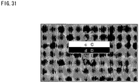
- display unevenness is explained below with reference to Figs. 30 through 35 .
- Fig. 30 shows an example of a display (stripe pattern of black and white lines surrounded by gray) image that is supposed to be displayed.
- the letters a to f and A to F each correspond to a single pixel. That is, the pixels a, b, e, f, A, B, E, and F display gray, the pixels c and C display white, and the pixels d and D display black.
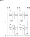
- Fig. 32 is an equivalent circuit diagram showing part of a configuration of a conventional liquid crystal panel.
- the pixels 101 to 106 correspond to the pixels a to f of Fig. 31 , respectively
- the pixels 111 to 116 correspond to the pixels A to F of Fig. 31 , respectively.
- Fig. 33 is an equivalent circuit diagram showing the appearance of parasitic capacitances produced in the pixels 101, 102, 111, and 112.
- Fig. 33 shows that the pixel 101 has a parasitic capacitance Csd_aq produced between a pixel electrode 17a and a data signal line 15q and a parasitic capacitance Csd_aQ produced between the pixel electrode 17a and a data signal line 15Q, that the pixel 102 has a parasitic capacitance Csd_bq produced between a pixel electrode 17b and the data signal line 15q and a parasitic capacitance Csd_bQ produced between the pixel electrode 17b and the data signal line 15Q, that the pixel 111 has a parasitic capacitance Csd_Ar produced between a pixel electrode 17A and a data signal line 15r and a parasitic capacitance Csd_AR produced between the pixel electrode 17A and a data signal line 15R, and
- Fig. 34 is a timing chart showing a method (normally black mode) for driving a liquid crystal panel in displaying the image of Fig. 31 .
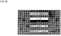
- Fig. 35 shows a display image that is displayed by the driving method.
- the reference sings Sp, SP, Sq, SQ, Sr, and SR refer to data signals that are supplied to the data signal lines 15p, 15P, 15q, 15Q, 15r, and 15R (see Fig. 32 ), respectively
- the reference signs GPa, GPb, GPc, GPd, GPe, and GPf refer to gate signals (scanning signals) that are supplied to the scanning signal lines 16a, 16b, 16c, 16d, 16e, and 16f (see Fig.
- Va, Vb, VA, VB, Vc, Vd, Ve, and Vf refer to potentials (pixel potentials) of the pixels electrodes 17a, 17b, 17A, 17B, 17c, 17d, 17e, and 17f (see Fig. 32 ), respectively.
- two scanning signals are simultaneously selected at a time and each data signal line is supplied with a data signal whose polarity is reversed every single frame period, and during the same horizontal scanning period, two data signal lines (15p and 15P, 15q and 15Q, 15r and 15R) corresponding to the same column of pixels are supplied with data signals of opposite polarities while two adjacent data signal lines (15P and 15q, 15Q and 15r, 15R and 15s) are supplied with data signals of the same polarity.
- the data signal line 15p, the data signal line 15Q, and the data signal line 15r are each supplied with a data signal of a positive polarity during the kth horizontal scanning period (including the scanning period for the scanning signal lines 16a and 16b), supplied with a data signal of a positive polarity during the (k+1)th horizontal scanning period (including the scanning period for the scanning signal lines 16c and 16d), and also supplied with a data signal of a positive polarity during the (k+2)th horizontal scanning period (including the scanning period for the scanning signal lines 16e and 16f).
- the data signal line 15P, the data signal line 15q, and the data signal line 15R are each supplied with a data signal of a negative polarity during the kth horizontal scanning period (including the scanning period for the scanning signal lines 16a and 16b), supplied with a data signal of a negative polarity during the (k+1)th horizontal scanning period (including the scanning period for the scanning signal lines 16c and 16d), and also supplied with a data signal of a negative polarity during the (k+2)th horizontal scanning period (including the scanning period for the scanning signal lines 16e and 16f).
- the data signal line 15p, the data signal line 15Q, and the data signal line 15r are each supplied with a data signal of a negative polarity during the kth horizontal scanning period (including the scanning period for the scanning signal lines 16a and 16b), supplied with a data signal of a negative polarity during the (k+1)th horizontal scanning period (including the scanning period for the scanning signal lines 16c and 16d), and also supplied with a data signal of a negative polarity during the (k+2)th horizontal scanning period (including the scanning period for the scanning signal lines 16e and 16f).
- the data signal line 15P, the data signal line 15q, and the data signal line 15R are each supplied with a data signal of a positive polarity during the kth horizontal scanning period (including the scanning period for the scanning signal lines 16a and 16b), supplied with a data signal of a positive polarity during the (k+1)th horizontal scanning period (including the scanning period for the scanning signal lines 16c and 16d), and also supplied with a data signal of a positive polarity during the (k+2)th horizontal scanning period (including the scanning period for the scanning signal lines 16e and 16f).
- the image of Fig. 31 is displayed (a) by, during the kth horizontal scanning period, supplying the pixel electrodes 17a and 17b, respectively connected to the scanning signal lines 16a and 16b simultaneously selected, with data signals (the pixel electrode 17a being supplied with a data signal of a negative polarity corresponding to gray, the pixel electrode 17b being supplied with a data signal of a positive polarity corresponding to gray) of opposite polarities and of equal magnitude (absolute value of voltage), (b) by, during the (k+1)th horizontal scanning period, supplying the pixel electrodes 17c and 17d, respectively connected to the scanning signal lines 16c and 16d simultaneously selected, with data signals (the pixel electrode 17c being supplied with a data signal of a negative polarity corresponding to white, the pixel electrode 17d being supplied with a data signal of a positive polarity corresponding to black) of opposite polarities and of different in magnitude (absolute value of voltage), and (c) by, during the (k+
- the data signal line 15q is supplied with a data signal of a negative polarity corresponding to gray during the kth horizontal scanning period, is supplied with a data signal of a negative polarity corresponding to white during the (k+1)th horizontal scanning period, and is supplied with a data signal of a negative polarity corresponding to gray during the (k+2)th horizontal scanning period.
- the data signal line 15Q is supplied with a data signal of a positive polarity corresponding to gray during the kth horizontal scanning period, is supplied with a data signal of a positive polarity corresponding to black during the (k+1)th horizontal scanning period, and is supplied with a data signal of a positive polarity corresponding to gray during the (k+2)th horizontal scanning period.
- the potentials of the data signals that are supplied to the data signal lines 15q and 15Q change in a falling direction (negative direction)
- the potentials of the data signals that are supplied to the data signal lines 15q and 15Q change in a rising direction (positive direction).
- the pixel potential Va (data signal of a negative polarity corresponding to gray) written during the kth horizontal scanning period changes in a falling direction (negative direction) in the (k+1)th horizontal scanning period due to the parasitic capacitances Csd_aq and Csd_aQ between the pixel electrode 17a and the data signal lines 15q and 15Q, respectively, and changes in a rising direction (positive direction) in the (k+2)th horizontal scanning period due to the parasitic capacitances Csd_aq and Csd_aQ between the pixel electrode 17a and the data signal lines 15q and 15Q, respectively (see Fig. 34 ).
- the pixel potential Vb (data signal of a positive polarity corresponding to gray) written during the kth horizontal scanning period changes in a falling direction (negative direction) in the (k-1)th horizontal scanning period due to the parasitic capacitances Csd_bq and Csd_bQ between the pixel electrode 17b and the data signal lines 15q and 15Q, respectively, and changes in a rising direction (positive direction) in the (k+2)th horizontal scanning period due to the parasitic capacitances Csd_aq and Csd_aQ between the pixel electrode 17b and the data signal lines 15q and 15Q, respectively (see Fig. 34 ).
- the pixel potential Ve (data signal of a positive polarity corresponding to gray) written during the previous frame period changes in a falling direction (negative direction) in the (k+1)th horizontal scanning period due to the parasitic capacitances Csd_eq and Csd_eQ (not illustrated) between the pixel electrode 17e and the data signal lines 15q and 15Q, respectively (see Fig. 34 ).
- the pixel potential Vf (data signal of a negative polarity corresponding to gray) written during the previous frame period changes in a falling direction (negative direction) in the (k+1)th horizontal scanning period due to the parasitic capacitances Csd_fq and Csd_fQ (not illustrated) between the pixel electrode 17f and the data signal lines 15q and 15Q, respectively (see Fig. 34 ).
- the pixel a which contains the pixel electrode 17a
- the pixel b which contains the pixel electrode 17b
- the pixel e which contains the pixel electrode 17e
- the pixel f which contains the pixel electrode 17f
- the present invention has as an object to enhance the display quality of a display device having a plurality of data signal lines provided for each column of pixels.
- a display device including: a plurality of scanning signal lines; and a plurality of data signal lines, two of which are provided for each column of pixels containing a plurality of pixels arranged in a column-wise direction in which the data signal lines extend, in each column of pixels, a pixel electrode contained in either of two pixels adjacent to each other in the column-wise direction and a pixel electrode contained in the other one of the two pixels adjacent to each other being connected to different data signal lines via transistors, respectively, for a first, a second, and a third columns of pixels arranged in sequence, each pixel electrode contained in the second column of pixels forming a capacitance with either of the two data signal lines provided for the first column of pixels and forming a capacitance with either of the two data signal lines provided for the third column of pixels.
- the influence of a crosstalk due to parasitic capacitances formed between each pixel electrode and data signal lines corresponding to the pixel, respectively, can be curbed by capacitances formed between that pixel electrode and data signal lines corresponding to both adjacent columns of pixels, respectively. This makes it possible to suppress a change in pixel potential in each pixel electrode and thus enhance the display quality of the liquid crystal display apparatus.
- a liquid crystal device is configured such that for a first, a second, and a third columns of pixels arranged in sequence, each pixel electrode contained in the second column of pixels forms a capacitance with either of the two data signal lines provided for the first column of pixels and forms a capacitance with either of the two data signal lines provided for the third column of pixels.
- the term “column-wise direction” means the direction in which the data signal lines extend and the term “row-wise direction” means the direction in which the scanning signal lines extend.
- the scanning signal lines may extend in a transverse direction or in a longitudinal direction.
- each pixel region of the active-matrix substrate corresponds to a single pixel of the liquid crystal panel.
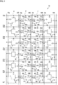
- Fig. 1 is an equivalent circuit diagram showing part of a liquid crystal panel according to the present embodiment.
- the present liquid crystal panel 10 has data signal lines 15p, 15P, 15q, 15Q, 15r, 15R, 15s, and 15S arranged in this order, and has scanning signal lines 16a, 16b, 16c, 16d, 16e, and 16f extending in the row-wise direction (in the drawing, a horizontal direction) and arranged in this order.
- the present liquid crystal panel 10 has a pixel 101 provided at intersections between the data signal lines 15q and 15Q and the scanning signal line 16a, a pixel 102 provided at intersections between the data signal lines 15q and 15Q and the scanning signal line 16b, and a pixel 103 provided at intersections between the data signal lines 15q and 15Q and the scanning signal line 16c.
- the present liquid crystal panel 10 also has pixels 104, 105, and 106 provided in similar manners.
- the present liquid crystal panel 10 has a pixel 111 provided at intersections between the data signal lines 15r and 15R and the scanning signal line 16a, a pixel 112 provided at intersections between the data signal lines 15r and 15R and the scanning signal line 16b, and a pixel 113 provided at intersections between the data signal lines 15r and 15R and the scanning signal line 16c.
- the present liquid crystal panel 10 also has pixels 114, 115, and 116 provided in similar manners.
- the present liquid crystal panel 10 has a retention capacitor wire 18a provided for the pixels 101 and 111, a retention capacitor wire 18b provided for the pixels 102 and 112, a retention capacitor wire 18c provided for the pixels 103 and 113, a retention capacitor wire 18d provided for the pixels 104 and 114, a retention capacitor wire 18e provided for the pixels 105 and 115, and a retention capacitor wire 18f provided for the pixels 106 and 116.
- the data signal lines 15p and 15P correspond to a column of pixels ⁇ (first column of pixels) containing a plurality of pixels arranged in the column-wise direction
- the data signal lines 15q and 15Q correspond to a column of pixels ⁇ (second column of pixels) containing the pixels 101 to 106
- the data signal lines 15r and 15R correspond to a column of pixels ⁇ (third column of pixels) containing the pixels 111 to 116.
- each pixel is provided with a pixel electrode.
- the pixel 101 has its pixel electrode 17a connected to the data signal line 15q via a transistor 12a connected to the scanning signal line 16a.
- the pixel 102 has its pixel electrode 17b connected to the data signal line 15Q via a transistor 12b connected to the scanning signal line 16b.
- the pixel 103 has its pixel electrode 17c connected to the data signal line 15q via a transistor 12c connected to the scanning signal line 16c.
- the pixel 104 has its pixel electrode 17d connected to the data signal line 15Q via a transistor 12d connected to the scanning signal line 16d.
- the pixel 105 has its pixel electrode 17e connected to the data signal line 15q via a transistor 12e connected to the scanning signal line 16e.
- the pixel 106 has its pixel electrode 17f connected to the data signal line 15Q via a transistor 12f connected to the scanning signal line 16f.
- the pixel 111 has its pixel electrode 17A connected to the data signal line 15r via a transistor 12A connected to the scanning signal line 16a.
- the pixel 112 has its pixel electrode 17B connected to the data signal line 15R via a transistor 12B connected to the scanning signal line 16b.
- the pixel 113 has its pixel electrode 17C connected to the data signal line 15r via a transistor 12C connected to the scanning signal line 16c.
- the pixel 114 has its pixel electrode 17D connected to the data signal line 15R via a transistor 12D connected to the scanning signal line 16d.
- the pixel 115 has its pixel electrode 17E connected to the data signal line 15r via a transistor 12E connected to the scanning signal line 16e.
- the pixel 116 has its pixel electrode 17F connected to the data signal line 15R via a transistor 12F connected to the scanning signal line 16f.
- the data signal line 15Q connected to the respective pixel electrodes (17b, 17d, 17f) of the even-numbered pixels (102, 104, 106) of the column of pixels ⁇
- the data signal line 15r connected to the respective pixel electrodes (17a, 17c, 17e) of the odd-numbered pixels (111, 113, 115) of the column of pixels ⁇ , are adjacent to each other.
- the scanning signal line 16a which corresponds to the pixel electrode 17a of the pixel 101 and the pixel electrode 17A of the pixel 111
- the scanning signal line 16b which corresponds to the pixel electrode 17b of the pixel 102 and the pixel electrode 17B of the pixel 112 are electrically connected to each other inside or outside of the panel, so that the scanning signal lines 16a and 16b are simultaneously selected.
- the scanning signal line 16c which corresponds to the pixel electrode 17c of the pixel 103 and the pixel electrode 17C of the pixel 113
- the scanning signal line 16d which corresponds to the pixel electrode 17d of the pixel 104 and the pixel electrode 17D of the pixel 114, are electrically connected to each other inside or outside of the panel, so that the scanning signal lines 16c and 16d are simultaneously selected.
- the scanning signal line 16e which corresponds to the pixel electrode 17e of the pixel 105 and the pixel electrode 17E of the pixel 115
- the scanning signal line 16f which corresponds to the pixel electrode 17f of the pixel 106 and the pixel electrode 17F of the pixel 116
- each of the pairs of scanning signal lines namely the scanning signal lines 16a and 16b, the scanning signal lines 16c and 16d, or the scanning signal lines 16e and 16f, are simultaneously selected without being electrically connected to each other inside or outside of the panel.
- the liquid crystal panel 10 thus configured has a retention capacitance Cha formed between the retention capacitor wire 18a and the pixel electrode 17a, a retention capacitance Chb formed between the retention capacitor wire 18b and the pixel electrode 17b, a retention capacitance Chc formed between the retention capacitor wire 18c and the pixel electrode 17c, a retention capacitance Chd formed between the retention capacitor wire 18d and the pixel electrode 17d, a retention capacitance Che formed between the retention capacitor wire 18e and the pixel electrode 17e, and a retention capacitance Chf formed between the retention capacitor wire 18f and the pixel electrode 17f.
- the liquid crystal panel 10 thus configured has a retention capacitance ChA formed between the retention capacitor wire 18a and the pixel electrode 17A, a retention capacitance ChB formed between the retention capacitor wire 18b and the pixel electrode 17B, a retention capacitance ChC formed between the retention capacitor wire 18c and the pixel electrode 17C, a retention capacitance ChD formed between the retention capacitor wire 18d and the pixel electrode 17D, a retention capacitance ChE formed between the retention capacitor wire 18e and the pixel electrode 17E, and a retention capacitance ChF formed between the retention capacitor wire 18f and the pixel electrode 17F.
- ChA formed between the retention capacitor wire 18a and the pixel electrode 17A
- a retention capacitance ChB formed between the retention capacitor wire 18b and the pixel electrode 17B
- a retention capacitance ChC formed between the retention capacitor wire 18c and the pixel electrode 17C
- a retention capacitance ChD formed between the retention capacitor wire 18d and the pixel electrode 17D
- parasitic capacitances are produced between the pixel electrodes and the data signal lines for structural reasons. That is, the pixel 101 has the parasitic capacitance Csd_aq produced between the pixel electrode 17a and the data signal line 15q and the parasitic capacitance Csd_aQ produced between the pixel electrode 17a and the data signal line 15Q.
- the pixel 102 has the parasitic capacitance Csd_bq produced between the pixel electrode 17b and the data signal line 15q and the parasitic capacitance Csd_bQ produced between the pixel electrode 17b and the data signal line 15Q.
- the pixel 111 has a parasitic capacitance Csd_Ar produced between the pixel electrode 17A and the data signal line 15r and a parasitic capacitance Csd_AR produced between the pixel electrode 17A and the data signal line 15R.
- the pixel 112 has a parasitic capacitance Csd_Br produced between the pixel electrode 17B and the data signal line 15r and a parasitic capacitance Csd_BR produced between the pixel electrode 17B and the data signal line 15R.
- Fig. 1 omits to illustrate the parasitic capacitances.
- the present invention has a configuration in which such changes in pixel potential are suppressed by each pixel electrode's forming a capacitance with each of the data signal lines respectively corresponding to both adjacent columns of pixels.
- Fig. 1 shows that the pixel 101 has a capacitance CaP formed between the pixel electrode 17a and the data signal line 15P and a capacitance Car formed between the pixel electrode 17a and the data signal line 15r, that the pixel 102 has a capacitance CbP formed between the pixel electrode 17b and the data signal line 15P and a capacitance Cbr formed between the pixel electrode 17b and the data signal line 15r, that the pixel 103 has a capacitance CcP formed between the pixel electrode 17c and the data signal line 15P and a capacitance Ccr formed between the pixel electrode 17c and the data signal line 15r, that the pixel 104 has a capacitance CdP formed between the pixel electrode 17d and the data signal line 15P and a capacitance Cdr formed between the pixel electrode 17d and the data signal line 15r, that the pixel 105 has a capacitance CeP formed between the pixel electrode 17e and the data signal line 15P and
- the pixel 111 has a capacitance CAQ formed between the pixel electrode 17A and the data signal line 15Q and a capacitance CAs formed between the pixel electrode 17A and the data signal line 15s.
- the pixel 112 has a capacitance CBQ formed between the pixel electrode 17B and the data signal line 15Q and a capacitance CBs formed between the pixel electrode 17B and the data signal line 15s.
- the pixel 113 has a capacitance CCQ formed between the pixel electrode 17C and the data signal line 15Q and a capacitance CCs formed between the pixel electrode 17C and the data signal line 15s.
- the pixel 114 has a capacitance CDQ formed between the pixel electrode 17d and the data signal line 15Q and a capacitance CDs formed between the pixel electrode 17D and the data signal line 15s.
- the pixel 115 has a capacitance CEQ formed between the pixel electrode 17E and the data signal line 15Q and a capacitance CEs formed between the pixel electrode 17E and the data signal line 15s.
- the pixel 116 has a capacitance CFQ formed between the pixel electrode 17F and the data signal line 15Q and a capacitance CFs formed between the pixel electrode 17F and the data signal line 15s.
- Fig. 2 is an equivalent circuit diagram showing the appearance of the capacitances formed in the pixels 101, 102, 111, and 112 of the present liquid crystal panel.
- each pixel electrode forms parasitic capacitances with the data signal lines corresponding to the pixel, respectively, and forms capacitances with the data signal lines corresponding to both adjacent columns of pixels, respectively.
- the pixel electrode 17b forms the parasitic capacitances Csd_bq and Csd_bQ with the data signal lines 15q and 15Q corresponding to the pixel 102, respectively, and forms the capacitances CbP and Cbr with the data signal lines 15P and 15r corresponding to both adjacent columns of pixels ⁇ and ⁇ , respectively.
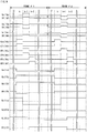
- Fig. 3 is a timing chart showing a method (normally black mode) for driving the liquid crystal panel of Fig. 1 .
- the reference sings Sp, SP, Sq, SQ, Sr, and SR refer to data signals that are supplied to the data signal lines 15p, 15P, 15q, 15Q, 15r, and 15R (see Fig. 1 ), respectively, that the reference signs GPa, GPb, GPc, GPd, GPe, and GPf refer to gate signals (scanning signals) that are supplied to the scanning signal lines 16a, 16b, 16c, 16d, 16e, and 16f (see Fig.
- Va, Vb, VA, VB, Vc, Vd, Ve, and Vf refer to potentials (pixel potentials) of the pixels electrodes 17a, 17b, 17A, 17B, 17c, 17d, 17e, and 17f (see Fig. 1 ), respectively.
- two scanning signals are simultaneously selected at a time and each data signal line is supplied with a data signal whose polarity is reversed every single frame period, and during the same horizontal scanning period, two data signal lines (15p and 15P, 15q and 15Q, 15r and 15R) corresponding to the same column of pixels are supplied with data signals of opposite polarities while two adjacent data signal lines (15P and 15q, 15Q and 15r, 15R and 15s) are supplied with data signals of the same polarity.
- the data signal line 15p, the data signal line 15Q, and the data signal line 15r are each supplied with a data signal of a positive polarity during the kth horizontal scanning period (including the scanning period for the scanning signal lines 16a and 16b), supplied with a data signal of a positive polarity during the (k+1)th horizontal scanning period (including the scanning period for the scanning signal lines 16c and 16d), and also supplied with a data signal of a positive polarity during the (k+2)th horizontal scanning period (including the scanning period for the scanning signal lines 16e and 16f).
- the data signal line 15P, the data signal line 15q, and the data signal line 15R are each supplied with a data signal of a negative polarity during the kth horizontal scanning period (including the scanning period for the scanning signal lines 16a and 16b), supplied with a data signal of a negative polarity during the (k+1)th horizontal scanning period (including the scanning period for the scanning signal lines 16c and 16d), and also supplied with a data signal of a negative polarity during the (k+2)th horizontal scanning period (including the scanning period for the scanning signal lines 16e and 16f).
- a pulse of the gate pulse signal (gate-on pulse signal) GPa and a pulse of the gate pulse signal GPb are raised.
- the pulses of GPa and GPb are dropped and a pulse of the gate pulse signal GPc and a pulse of the gate pulse signal GPd are raised.
- the pulses of GPc and GPd are dropped and a pulse of the gate pulse signal GPe and a pulse of the gate pulse signal GPf are raised.
- a data signal of a negative polarity, a data signal of a positive polarity, a data signal of a negative polarity, a data signal of a positive polarity, a data signal of a negative polarity, and a data signal of a positive polarity are written to the pixel electrode 17a of the pixel 101, the pixel electrode 17b of the pixel 102, the pixel electrode 17c of the pixel 103, the pixel electrode 17d of the pixel 104, the pixel electrode 17e of the pixel 105, and the pixel electrode 17f of the pixel 106, respectively.
- a data signal of a positive polarity, a data signal of a negative polarity, a data signal of a positive polarity, a data signal of a negative polarity, a data signal of a positive polarity, and a data signal of a negative polarity are written to the pixel electrode 17A of the pixel 111, the pixel electrode 17B of the pixel 112, the pixel electrode 17C of the pixel 113, the pixel electrode 17D of the pixel 114, the pixel electrode 17E of the pixel 115, and the pixel electrode 17F of the pixel 116, respectively.
- the data signal line 15p, the data signal line 15Q, and the data signal line 15r are each supplied with a data signal of a negative polarity during the kth horizontal scanning period (including the scanning period for the scanning signal lines 16a and 16b), supplied with a data signal of a negative polarity during the (k+1)th horizontal scanning period (including the scanning period for the scanning signal lines 16c and 16d), and also supplied with a data signal of a negative polarity during the (k+2)th horizontal scanning period (including the scanning period for the scanning signal lines 16e and 16f).
- the data signal line 15P, the data signal line 15q, and the data signal line 15R are each supplied with a data signal of a positive polarity during the kth horizontal scanning period (including the scanning period for the scanning signal lines 16a and 16b), supplied with a data signal of a positive polarity during the (k+1)th horizontal scanning period (including the scanning period for the scanning signal lines 16c and 16d), and also supplied with a data signal of a positive polarity during the (k+2)th horizontal scanning period (including the scanning period for the scanning signal lines 16e and 16f).
- the pulse of the gate pulse signal (gate-on pulse signal) GPa and the pulse of the gate pulse signal GPb are raised.
- the pulses of GPa and GPb are dropped and a pulse of the gate pulse signal GPc and a pulse of the gate pulse signal GPd are raised.
- the pulses of GPc and GPd are dropped and a pulse of the gate pulse signal GPe and a pulse of the gate pulse signal GPf are raised.
- a data signal of a positive polarity, a data signal of a negative polarity, a data signal of a positive polarity, a data signal of a negative polarity, a data signal of a positive polarity, and a data signal of a negative polarity are written to the pixel electrode 17a of the pixel 101, the pixel electrode 17b of the pixel 102, the pixel electrode 17c of the pixel 103, the pixel electrode 17d of the pixel 104, the pixel electrode 17e of the pixel 105, and the pixel electrode 17f of the pixel 106, respectively.
- a data signal of a negative polarity, a data signal of a positive polarity, a data signal of a negative polarity, a data signal of a positive polarity, a data signal of a negative polarity, and a data signal of a positive polarity are written to the pixel electrode 17A of the pixel 111, the pixel electrode 17B of the pixel 112, the pixel electrode 17C of the pixel 113, the pixel electrode 17D of the pixel 114, the pixel electrode 17E of the pixel 115, and the pixel electrode 17F of the pixel 116, respectively.
- the above driving method achieves dot-reversal driving.
- the image of Fig. 31 is displayed (a) by, during the kth horizontal scanning period, supplying the pixel electrodes 17a and 17b, respectively connected to the scanning signal lines 16a and 16b simultaneously selected, with data signals (the pixel electrode 17a being supplied with a data signal of a negative polarity corresponding to gray, the pixel electrode 17b being supplied with a data signal of a positive polarity corresponding to gray) of opposite polarities and of equal magnitude (absolute value of voltage), (b) by, during the (k+1)th horizontal scanning period, supplying the pixel electrodes 17c and 17d, respectively connected to the scanning signal lines 16c and 16d simultaneously selected, with data signals (the pixel electrode 17c being supplied with a data signal of a negative polarity corresponding to white, the pixel electrode 17b being supplied with a data signal of a positive polarity corresponding to black) of opposite polarities and of equal magnitude (absolute value of voltage), and (c) by, during the (k+2)
- the data signal line 15q is supplied with a data signal of a negative polarity corresponding to gray during the kth horizontal scanning period, is supplied with a data signal of a negative polarity corresponding to white during the (k+1)th horizontal scanning period, and is supplied with a data signal of a negative polarity corresponding to gray during the (k+2)th horizontal scanning period.
- the data signal line 15Q is supplied with a data signal of a positive polarity corresponding to gray during the kth horizontal scanning period, is supplied with a data signal of a positive polarity corresponding to black during the (k+1)th horizontal scanning period, and is supplied with a data signal of a positive polarity corresponding to gray during the (k+2)th horizontal scanning period.
- the potentials of the data signals that are supplied to the data signal lines 15q and 15Q change in a falling direction (negative direction)
- the potentials of the data signals that are supplied to the data signal lines 15q and 15Q change in a rising direction (positive direction).
- the pixel potential Va (data signal of a negative polarity corresponding to gray) written during the kth horizontal scanning period changes in a falling direction (negative direction) in the (k+1)th horizontal scanning period due to the parasitic capacitances Csd_aq and Csd_aQ between the pixel electrode 17a and the data signal lines 15q and 15Q, respectively, and changes in a rising direction (positive direction) in the (k+2)th horizontal scanning period due to the parasitic capacitances Csd_aq and Csd_aQ between the pixel electrode 17a and the data signal lines 15q and 15Q, respectively (see Fig. 34 ).
- the pixel electrode 17a forms capacitances CaP and Car with the data signal lines 15P and 15r, respectively.
- the data signal line 15P is supplied with a data signal of a negative polarity corresponding to gray during the kth horizontal scanning period, is supplied with a data signal of a negative polarity corresponding to black during the (k+1)th horizontal scanning period, and is supplied with a data signal of a negative polarity corresponding to gray during the (k+2)th horizontal scanning period.
- the data signal line 15r is supplied with a data signal of a positive polarity corresponding to gray during the kth horizontal scanning period, is supplied with a data signal of a positive polarity corresponding to white during the (k+1)th horizontal scanning period, and is supplied with a data signal of a positive polarity corresponding to gray during the (k+2)th horizontal scanning period.
- the pixel potential Va data signal of a negative polarity corresponding to gray
- the changes in potential due to the parasitic capacitances can be canceled by the changes in potential due to the capacitances formed between the pixel electrode and the data signal lines corresponding to both adjacent columns of pixels, respectively. This makes it possible to curb the influence of a crosstalk and thus enhance display quality.
- the pixel potential Vb (data signal of a positive polarity corresponding to gray) written during the kth horizontal scanning period changes in a falling direction (negative direction) due to the parasitic capacitances Csd_bq and Csd_bQ between the pixel electrode 17b and the data signal lines 15q and 15Q, respectively (see Fig.
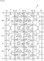
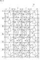
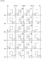
- Fig. 5 is a plan view showing a configuration of the liquid crystal panel of Fig. 1 .
- the present liquid crystal panel 10 has a pair of (two) data signal lines 15q and 15Q and a pair of (two) data signal lines 15r and 15R provided so that the data signal line 15Q and the data signal line 15r are adjacent to each other, has scanning signal lines 16a and 16b provided in such a way as to be orthogonal to the data signal lines, has a transistor 12a provided near an intersection between the data signal line 15q and the scanning signal line 16a, has a transistor 12b provided near an intersection between the data signal line 15Q and the scanning signal line 16b, has a transistor 12A provided near an intersection between the data signal line 15r and the scanning signal line 16a, and has a transistor 12B provided near an intersection between the data signal line 15R and the scanning signal line 16b.
- the present liquid crystal panel 10 has a pixel electrode 17a provided so that part thereof overlaps the data signal lines 15P, 15q, 15Q, and 15r, a pixel electrode 17b provided so that part thereof overlaps the data signal lines 15P, 15q, 15Q, and 15r, a pixel electrode 17A provided so that part thereof overlaps the data signal lines 15Q, 15r, 15R, and 15s, and a pixel electrode 17B provided so that part thereof overlaps the data signal lines 15Q, 15r, 15R, and 15s.
- the present liquid crystal panel 10 has a retention capacitor wire 18a provided in such a way as to overlap the pixel electrodes 17a and 17A and a retention capacitor wire 18b provided in such a way as to overlap the pixel electrodes 17b and 17B.
- the scanning signal line 16a functions as the gate electrode of the transistor 12a, which has its source electrode connected to the data signal line 15q and which has its drain electrode connected to a capacitor electrode 37a via a drain drawing electrode 27a.
- the capacitor electrode 37a is provided above the retention capacitor wire 18a and is connected to the pixel electrode 17a via a contact hole 11a.
- the scanning signal line 16b functions as the gate electrode of the transistor 12b, which has its source electrode connected to the data signal line 15Q and which has its drain electrode connected to a capacitor electrode 37b via a drain drawing electrode 27b.
- the capacitor electrode 37b is provided above the retention capacitor wire 18b and is connected to the pixel electrode 17b via a contact hole 11b.
- the scanning signal line 16a functions as the gate electrode of the transistor 12A, which has its source electrode connected to the data signal line 15r and which has its drain electrode connected to a capacitor electrode 37A via a drain drawing electrode 27A.
- the capacitor electrode 37A is provided above the retention capacitor wire 18A and is connected to the pixel electrode 17A via a contact hole 11A.
- the scanning signal line 16b functions as the gate electrode of the transistor 12B, which has its source electrode connected to the data signal line 15R and which has its drain electrode connected to a capacitor electrode 37B via a drain drawing electrode 27B.
- the capacitor electrode 37B is provided above the retention capacitor wire 18b and is connected to the pixel electrode 17B via a contact hole 11B.
- the present liquid crystal panel 10 is configured such that the retention capacitance Cha (see Fig. 1 ) is formed in a portion where the retention capacitor wire 18a and the capacitor electrode 37a overlap each other via a gate insulating film, that the retention capacitance Chb (see Fig. 1 ) is formed in a portion where the retention capacitor wire 18b and the capacitor electrode 37b overlap each other via the gate insulating film, that the retention capacitance ChA (see Fig. 1 ) is formed in a portion where the retention capacitor wire 18a and the capacitor electrode 37A overlap each other via the gate insulating film, and that the retention capacitance ChB (see Fig. 1 ) is formed in a portion where the retention capacitor wire 18b and the capacitor electrode 37B overlap each other via the gate insulating film.
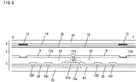
- Fig. 6 is a cross-sectional view taken along the arrow X-Y of Fig. 5 .
- the present liquid crystal panel 10 includes: an active-matrix substrate 3; a color filter substrate 4 placed opposite the active-matrix substrate 3; and a liquid crystal layer 5 placed between the substrates 3 and 4.
- the active-matrix substrate 3 has a glass substrate 32 on which the scanning signal line 16a (not illustrated) and the retention capacitor wire 18a have been formed, with a gate insulating film 43 formed so as to cover the scanning signal line 16a and the retention capacitor wire 18a.
- the capacitor electrode 37a Formed on the gate insulating film 43 are the capacitor electrode 37a, the data signal lines 15P, 15q, 15Q, and 15r, and the drain drawing electrode 27a (not illustrated). Further formed on the gate insulating film 43 are semiconductor layers (an i layer and an n+ layer) of each transistor and source and drain electrodes that are in contact with the n+ layer, although not illustrated. Furthermore, the active matrix substrate 3 has an inorganic interlayer insulating film 25 formed in such a way as to cover a metal layer containing each data signal line and an inorganic interlayer insulating film 26 formed on the inorganic interlayer insulating film 25, the inorganic interlayer insulating film 26 being thicker than the inorganic interlayer insulating film 25.
- the pixel electrodes 17a and 17A are covered by an alignment film 9.
- the inorganic interlayer insulating film 25 and the organic interlayer insulating film 26 are bored through, so that the pixel electrode 17a and the capacitor electrode 37a are in contact with each other.
- the retention capacitance Cha is formed in a portion where the retention capacitor wire 18a and the capacitor electrode 37a overlap each other via the gate insulating film 43.
- the capacitance CaP (see Figs.
- the color filter substrate 4 has a glass substrate 41 on which a black matrix 13 and a colored layer (color filter layer) 14 have been formed, with a common electrode (com) 28 formed on the black matrix 13 and the color filter layer 14 and covered with an alignment film 19.
- a configuration may be such that writing to each pixel electrode is carried out by sequentially (one by one) selecting scanning signal lines corresponding to each separate pixel.
- the method for fabricating a liquid crystal panel includes an active-matrix substrate fabricating step, a color filter substrate fabricating step, and an assembling step of joining the substrates on top of each other and filling a space between the substrates with liquid crystals.
- a metal film made of titanium, chromium, aluminum, molybdenum, tantalum, tungsten, copper, or the like, an alloy film made of an alloy thereof, or a laminate film (1000 ⁇ to 3000 ⁇ thick) obtained by joining such films on top of each other is formed by sputtering on a substrate made of glass, plastic, or the like.
- patterning is carried out by a photolithographic technique (photo engraving process, hereinafter referred to as "PEP technique", which includes an etching step), so that scanning signal lines (gate electrode of each transistor) and retention capacitor wires are formed.
- an inorganic insulating film (approximately 3000 ⁇ to 5000 ⁇ thick) of silicon nitride, silicon oxide, or the like is formed by CVD (chemical vapor deposition) over the entire substrate on which the scanning signal lines have been formed, and the photoresist is removed, so that a gate insulating film is formed.
- CVD chemical vapor deposition
- an intrinsic amorphous silicon film (1000 ⁇ to 3000 ⁇ thick) and an n+ amorphous silicon film (approximately 400 ⁇ to 700 ⁇ thick) doped with phosphor are continuously formed by CVD over the gate insulating film (entire substrate).
- patterning is carried out by the PEP technique, and the photoresist is removed, so that a silicon laminate constituted by the intrinsic amorphous silicon layer and the n+ amorphous silicon layer is formed in the form of an island on the gate electrode.
- a metal film made of titanium, chromium, aluminum, molybdenum, tantalum, tungsten, copper, or the like, an alloy film made of an alloy thereof, or a laminate film (1000 ⁇ to 3000 ⁇ thick) obtained by joining such films on top of each other is formed by sputtering over the entire substrate on which the silicon laminate has been formed.
- patterning is carried out by the PEP technique, so that data signal lines, the source and drain electrodes of transistors, drain drawing electrodes, capacitor electrodes, and drawing wires are formed (formation of a metal layer).
- the resist is removed as needed here.
- the photoresist used in formed the metal wires or the source and drain electrodes is etched away, and the photoresist is removed, so that channels in the transistors are formed.
- the semiconductor layer may be formed by an amorphous silicon film as described above, but a polysilicon film may also be formed.
- improvements in crystallinity can be made by performing a laser anneal process on the amorphous silicon film and the polysilicon film. This makes it possible to improve the characteristics of each transistor (TFT) with an increase in speed at which electrons move within the semiconductor layer.
- an interlayer insulating film is formed over the entire substrate on which the data signal lines and the like have been formed.
- an inorganic interlayer insulating film (passivation film) made of SiNx approximately 300 ⁇ thick is formed by CVD in such a way as to cover the entire surface of the substrate, and furthermore, an organic interlayer insulting film made of a positive photosensitive acrylic resin approximately 3 ⁇ m thick is formed by spin coating or die coating.
- the organic interlayer insulating film is patterned with contact holes by the PEP techniques, and then sintered. Furthermore, by using the pattern on the organic interlayer insulating film, the inorganic interlayer insulating film or the inorganic interlayer insulating film and the gate insulating film is/are etched away, so that the contact holes are formed.
- a transparent conductive film (1000 ⁇ to 2000 ⁇ thick) made of ITO (indium tin oxide), IZO (indium zinc oxide), zinc oxide, tin oxide, or the like is formed by sputtering on the interlayer insulating film over the entire substrate in which the contact holes have been formed. After that, patterning is carried out by the PEP technique, and the resist is removed, so that each pixel electrode is formed.
- a polyimide resin 500 ⁇ to 1000 ⁇ thick is printed on the pixel electrodes over the entire substrate.
- the polyimide resin is calcined, and rubbed with rotating cloth in one direction, so that an alignment film is formed. This is how the active-matrix substrate is fabricated.
- a black matrix is formed by forming a chromium thin film or a film of resin containing a black pigment on a substrate (entire substrate) made of glass, plastic, or the like and patterning the film by the PEP technique.
- a red, green, and blue color filter layer (approximately 2 ⁇ m thick) is pattern-formed in spaces in the black matrix by using a pigment dispersion method.
- a common electrode is formed by forming a transparent conductive film (approximately 1000 ⁇ thick) made of ITO, IZO, zinc oxide, tin oxide, or the like on the color filter layer over the entire substrate.
- a polyimide resin 500 ⁇ to 1000 ⁇ thick is printed on the common electrode over the entire substrate. After that, the polyimide resin is calcined, and rubbed with rotating cloth in one direction, so that an alignment film is formed. This is how the color filter substrate is fabricated.
- a sealing material made of a thermosetting epoxy resin is applied by screen printing onto either the active-matrix substrate and the color filter substrate into a frame pattern lacking a part that serves as a liquid crystal inlet later, and spherical spacers each having a diameter equivalent to the thickness of the liquid crystal layer and made of plastic or silica are scattered on the other substrate. It is possible to form spacers on the black matrix of the color filter substrate or on the metal wires of the active-matrix substrate by the PEP technique instead of scattering spacers.
- the active-matrix substrate and the color filter substrate are joined on top of each other, and the sealing material is cured.
- the liquid crystal layer is formed by filling the space enclosed by the active-matrix substrate, the color filter, and the sealing material with a liquid crystal material by an evacuation method, applying a UV-curing resin to the liquid crystal inlet, and then sealing the liquid crystal material by UV irradiation. This is how the liquid crystal panel is fabricated.
- liquid crystal panel 10 shown in Fig. 1 may be configured in any one of the following manners. The following describes other configurations of the liquid crystal panel according to the present invention. For convenience of explanation, a description of components identical to those of the aforementioned liquid crystal panel is omitted as needed.
- Fig. 7 is an equivalent circuit diagram showing part of a configuration of a liquid crystal panel 20 in Example Configuration 2.
- the arrangement of the data signal lines, the scanning signal lines, the retention capacitor wires, and the pixels of the liquid crystal panel 20 of Fig. 7 is identical to that of the liquid crystal panel 10 of Fig. 1 .
- each pixel is provided with a pixel electrode.
- the pixel 101 has its pixel electrode 17a connected to the data signal line 15Q via a transistor 12a connected to the scanning signal line 16a.
- the pixel 102 has its pixel electrode 17b connected to the data signal line 15q via a transistor 12b connected to the scanning signal line 16b.
- the pixel 103 has its pixel electrode 17c connected to the data signal line 15Q via a transistor 12c connected to the scanning signal line 16c.
- the pixel 104 has its pixel electrode 17d connected to the data signal line 15q via a transistor 12d connected to the scanning signal line 16d.
- the pixel 105 has its pixel electrode 17e connected to the data signal line 15Q via a transistor 12e connected to the scanning signal line 16e.
- the pixel 106 has its pixel electrode 17f connected to the data signal line 15q via a transistor 12f connected to the scanning signal line 16f.
- the pixel 111 has its pixel electrode 17A connected to the data signal line 15r via a transistor 12A connected to the scanning signal line 16a.
- the pixel 112 has its pixel electrode 17B connected to the data signal line 15R via a transistor 12B connected to the scanning signal line 16b.
- the pixel 113 has its pixel electrode 17C connected to the data signal line 15r via a transistor 12C connected to the scanning signal line 16c.
- the pixel 114 has its pixel electrode 17D connected to the data signal line 15R via a transistor 12D connected to the scanning signal line 16d.
- the pixel 115 has its pixel electrode 17E connected to the data signal line 15r via a transistor 12E connected to the scanning signal line 16e.
- the pixel 116 has its pixel electrode 17F connected to the data signal line 15R via a transistor 12F connected to the scanning signal line 16f.
- the data signal line 15Q connected to the respective pixel electrodes (17a, 17c, 17e) of the odd-numbered pixels (101, 103, 105) of the column of pixels ⁇
- the data signal line 15r connected to the respective pixel electrodes (17A, 17C, 17E) of the odd-numbered pixels (111, 113, 115) of the column of pixels ⁇ , are adjacent to each other.
- Fig. 8 is an equivalent circuit diagram showing the appearance of the capacitances formed in the pixels 101, 102, 111, and 112 of the liquid crystal panel 20 shown in Fig. 7 .
- the pixel electrode 17b forms parasitic capacitances Csd_bq and Csd_bQ with the data signal lines 15q and 15Q corresponding to the pixel 102, respectively, and forms the capacitances CbP and Cbr with the data signal lines 15P and 15r corresponding to both adjacent columns of pixels ⁇ and ⁇ , respectively.
- Fig. 9 is a timing chart showing a method (normally black mode) for driving the liquid crystal panel 20 of Fig. 7 .
- Fig. 9 two scanning signals are simultaneously selected at a time and each data signal line is supplied with a data signal whose polarity is reversed every single frame period, and during the same horizontal scanning period, two data signal lines (15p and 15P, 15q and 15Q, 15r and 15R) corresponding to the same column of pixels are supplied with data signals of opposite polarities while two adjacent data signal lines (15P and 15q, 15Q and 15r, 15R and 15s) are supplied with data signals of opposite polarities. That is, a comparison with the driving method of Fig. 3 shows that the data signals Sq and SQ have been interchanged.
- a data signal of a negative polarity, a data signal of a positive polarity, a data signal of a negative polarity, a data signal of a positive polarity, a data signal of a negative polarity, and a data signal of a positive polarity are written to the pixel electrode 17a of the pixel 101, the pixel electrode 17b of the pixel 102, the pixel electrode 17c of the pixel 103, the pixel electrode 17d of the pixel 104, the pixel electrode 17e of the pixel 105, and the pixel electrode 17f of the pixel 106, respectively.
- a data signal of a positive polarity, a data signal of a negative polarity, a data signal of a positive polarity, a data signal of a negative polarity, a data signal of a positive polarity, and a data signal of a negative polarity are written to the pixel electrode 17A of the pixel 111, the pixel electrode 17B of the pixel 112, the pixel electrode 17C of the pixel 113, the pixel electrode 17D of the pixel 114, the pixel electrode 17E of the pixel 115, and the pixel electrode 17F of the pixel 116, respectively.
- a data signal of a positive polarity, a data signal of a negative polarity, a data signal of a positive polarity, a data signal of a negative polarity, a data signal of a positive polarity, and a data signal of a negative polarity are written to the pixel electrode 17a of the pixel 101, the pixel electrode 17b of the pixel 102, the pixel electrode 17c of the pixel 103, the pixel electrode 17d of the pixel 104, the pixel electrode 17e of the pixel 105, and the pixel electrode 17f of the pixel 106, respectively.
- a data signal of a negative polarity, a data signal of a positive polarity, a data signal of a negative polarity, a data signal of a positive polarity, a data signal of a negative polarity, and a data signal of a positive polarity are written to the pixel electrode 17A of the pixel 111, the pixel electrode 17B of the pixel 112, the pixel electrode 17C of the pixel 113, the pixel electrode 17D of the pixel 114, the pixel electrode 17E of the pixel 115, and the pixel electrode 17F of the pixel 116, respectively.
- the present driving method achieves dot-reversal driving.
- the data signal line 15q is supplied with a data signal of a positive polarity corresponding to gray during the kth horizontal scanning period, is supplied with a data signal of a positive polarity corresponding to black during the (k+1)th horizontal scanning period, and is supplied with a data signal of a positive polarity corresponding to gray during the (k+2)th horizontal scanning period.
- the data signal line 15Q is supplied with a data signal of a negative polarity corresponding to gray during the kth horizontal scanning period, is supplied with a data signal of a negative polarity corresponding to white during the (k+1)th horizontal scanning period, and is supplied with a data signal of a negative polarity corresponding to gray during the (k+2)th horizontal scanning period.
- the potentials of the data signals that are supplied to the data signal lines 15q and 15Q change in a falling direction (negative direction)
- the potentials of the data signals that are supplied to the data signal lines 15q and 15Q change in a rising direction (positive direction).
- the pixel potential Va (data signal of a negative polarity corresponding to gray) written during the kth horizontal scanning period changes in a falling direction (negative direction) in the (k+1)th horizontal scanning period due to the parasitic capacitances Csd_aq and Csd_aQ between the pixel electrode 17a and the data signal lines 15q and 15Q, respectively, and changes in a rising direction (positive direction) in the (k+2)th horizontal scanning period due to the parasitic capacitances Csd_aq and Csd_aQ between the pixel electrode 17a and the data signal lines 15q and 15Q, respectively (see Fig. 34 ).
- the pixel electrode 17a forms capacitances CaP and Car with the data signal lines 15P and 15r, respectively.
- the data signal line 15P is supplied with a data signal of a negative polarity corresponding to gray during the kth horizontal scanning period, is supplied with a data signal of a negative polarity corresponding to black during the (k+1)th horizontal scanning period, and is supplied with a data signal of a negative polarity corresponding to gray during the (k+2)th horizontal scanning period.
- the data signal line 15r is supplied with a data signal of a positive polarity corresponding to gray during the kth horizontal scanning period, is supplied with a data signal of a positive polarity corresponding to white during the (k+1)th horizontal scanning period, and is supplied with a data signal of a positive polarity corresponding to gray during the (k+2)th horizontal scanning period.
- the pixel potential Va data signal of a negative polarity corresponding to gray
- the pixel potential Va changes in a rising direction (positive direction) in the (k+1)th horizontal scanning period due to the capacitances CaP and Car, respectively, and changes in a falling direction (negative direction) in the (k+2)th horizontal scanning period due to the capacitances CaP and Car.
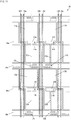
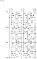
- Fig. 11 is a plan view showing Example Configuration 2 of the liquid crystal panel 20 of Fig. 7 .
- the present liquid crystal panel 20 has its transistor 12a provided near an intersection between the data signal line 15Q and the scanning signal line 16a, has its transistor 12b provided near an intersection between the data signal line 15q and the scanning signal line 16b, has its transistor 12A provided near an intersection between the data signal line 15r and the scanning signal line 16a, and has its transistor 12B provided near an intersection between the data signal line 15R and the scanning signal line 16b.
- the other components of the liquid crystal panel 20 of Fig. 7 are identical to those of the liquid crystal panel 10 of Fig. 5 .
- Fig. 12 is an equivalent circuit diagram showing part of a configuration of a liquid crystal panel 30 in Example Configuration 3.
- the liquid crystal panel 30 of Fig. 12 has data signal lines 15P, 15q, 15Q, 15r, 15R, and 15s arranged in this order, and has scanning signal lines 16ab, 16cd, and 16ef extending in the row-wise direction (in the drawing, a horizontal direction) and arranged in this order.
- the liquid crystal panel 30 has pixels 101 and 102 provided at intersections between the data signal lines 15q and 15Q and the scanning signal line 16ab, pixels 103 and 104 provided at intersections between the data signal lines 15q and 15Q and the scanning signal line 16cd, and pixels 105 and 106 provided at intersections between the data signal lines 15q and 15Q and the scanning signal line 16ef.
- the liquid crystal panel 30 has pixels 111 and 112 provided at intersections between the data signal lines 15r and 15R and the scanning signal line 16ab, pixels 113 and 114 provided at intersections between the data signal lines 15r and 15R and the scanning signal line 16cd, and pixels 115 and 116 provided at intersections between the data signal lines 15r and 15R and the scanning signal line 16ef.
- the liquid crystal panel 30 has a retention capacitor wire 18g provided for the pixels 101 and 111, a retention capacitor wire 18h provided for the pixels 102, 112, 103, and 113, a retention capacitor wire 18i provided for the pixels 104, 114, 105, and 115, a retention capacitor wire 18j provided for the pixels 106 and 116.
- the liquid crystal panel 30 has a retention capacitance Cha formed between the retention capacitor wire 18g and the pixel electrode 17a, a retention capacitance Chb formed between the retention capacitor wire 18h and the pixel electrode 17b, a retention capacitance Chc formed between the retention capacitor wire 18h and the pixel electrode 17c, a retention capacitance Chd formed between the retention capacitor wire 18i and the pixel electrode 17d, a retention capacitance Che formed between the retention capacitor wire 18i and the pixel electrode 17e, and a retention capacitance Chf formed between the retention capacitor wire 18j and the pixel electrode 17f.
- the liquid crystal panel 30 has a retention capacitance ChA formed between the retention capacitor wire 18g and the pixel electrode 17A, a retention capacitance ChB formed between the retention capacitor wire 18h and the pixel electrode 17B, a retention capacitance ChC formed between the retention capacitor wire 18h and the pixel electrode 17C, a retention capacitance ChD formed between the retention capacitor wire 18i and the pixel electrode 17D, a retention capacitance ChE formed between the retention capacitor wire 18i and the pixel electrode 17E, and a retention capacitance ChF formed between the retention capacitor wire 18j and the pixel electrode 17F.
- ChA formed between the retention capacitor wire 18g and the pixel electrode 17A
- ChB formed between the retention capacitor wire 18h and the pixel electrode 17B
- a retention capacitance ChC formed between the retention capacitor wire 18h and the pixel electrode 17C
- a retention capacitance ChD formed between the retention capacitor wire 18i and the pixel electrode 17D
- a retention capacitance ChE formed between the retention capacitor
- Fig. 13 is an equivalent circuit diagram showing the appearance of the capacitances formed in the pixels 101, 102, 103, 111, 112, and 113 of the liquid crystal panel 30 of Fig. 12 .
- the pixel electrode 17b forms parasitic capacitances Csd_bq and Csd_bQ with the data signal lines 15q and 15Q corresponding to the pixel 102, respectively, and forms the capacitances CbP and Cbr with the data signal lines 15P and 15r corresponding to both adjacent columns of pixels ⁇ and ⁇ , respectively.
- Fig. 14 is a timing chart showing a method (normally black mode) for driving the liquid crystal panel 30 of Fig. 12 .
- the reference sings GPab, GPcd, and GPef refer to data signals that are supplied to the scanning signal lines 16ab, 16cd, and 16ef, respectively.
- one scanning signal is selected at a time and each data signal line is supplied with a data signal whose polarity is reversed every single frame period, and during the same horizontal scanning period, two data signal lines (15p and 15P, 15q and 15Q, 15r and 15R) corresponding to the same column of pixels are supplied with data signals of opposite polarities while two adjacent data signal lines (15P and 15q, 15Q and 15r, 15R and 15s) are supplied with data signals of the same polarity. Changes in each separate pixel electrode are identical to those shown in the timing chart of Fig. 3 , and as such, are not described here.
- Fig. 15 is a plan view showing Example Configuration 3 of the liquid crystal panel 30 of Fig. 12 .
- the present liquid crystal panel 30 has a pair of (two) data signal lines 15q and 15Q and a pair of (two) data signal lines 15r and 15R provided so that the data signal line 15Q and the data signal line 15r are adjacent to each other, and has its scanning signal lines 16ab and 16cd provided in such a way as to be orthogonal to the data signal lines.
- the present liquid crystal panel 30 has its transistor 12a provided near an intersection between the data signal line 15q and the scanning signal line 16ab, has its transistor 12b provided near an intersection between the data signal line 15Q and the scanning signal line 16ab, has its transistor 12A provided near an intersection between the data signal line 15r and the scanning signal line 16ab, and has its transistor 12B provided near an intersection between the data signal line 15R and the scanning signal line 16ab.
- the present liquid crystal panel 30 has its transistor 12c provided near an intersection between the data signal line 15q and the scanning signal line 16cd, has its transistor 12d provided near an intersection between the data signal line 15Q and the scanning signal line 16cd, has its transistor 12C provided near an intersection between the data signal line 15r and the scanning signal line 16cd, and has its transistor 12D provided near an intersection between the data signal line 15R and the scanning signal line 16cd.
- the present liquid crystal panel 30 has its pixel electrodes 17a, 17b, 17c, and 17d provided so that parts thereof overlap the data signal lines 15P, 15q, 15Q, and 15r, respectively, and has its pixel electrodes 17A, 17B, 17C, and 17D provided so that parts thereof overlap the data signal lines 15Q, 15r, 15R, and 15s, respectively.
- the present liquid crystal panel 30 has its retention capacitor wire 18g provided in such a way as to overlap the pixel electrodes 17a and 17A, has its retention capacitor wire 18h provided in such a way as to overlap the pixel electrodes 17b, 17B, 17c, and 17C, and has its retention capacitor wire 18i provided in such a way as to overlap the pixel electrodes 17d and 17D.
- the scanning signal line 16ab functions as the gate electrode of the transistor 12a, which has its source electrode connected to the data signal line 15q and which has its drain electrode connected to a capacitor electrode 37a via a drain drawing electrode 27a.
- the capacitor electrode 37a is provided above the retention capacitor wire 18g and is connected to the pixel electrode 17a via a contact hole 11a.
- the scanning signal line 16ab functions as the gate electrode of the transistor 12b, which has its source electrode connected to the data signal line 15Q and which has its drain electrode connected to a capacitor electrode 37b via a drain drawing electrode 27b.
- the capacitor electrode 37b is provided above the retention capacitor wire 18h and is connected to the pixel electrode 17b via a contact hole 11b.
- the scanning signal line 16cd functions as the gate electrode of the transistor 12c, which has its source electrode connected to the data signal line 15q and which has its drain electrode connected to a capacitor electrode 37c via a drain drawing electrode 27c.
- the capacitor electrode 37c is provided above the retention capacitor wire 18h and is connected to the pixel electrode 17c via a contact hole 11c.
- the scanning signal line 16cd functions as the gate electrode of the transistor 12d, which has its source electrode connected to the data signal line 15Q and which has its drain electrode connected to a capacitor electrode 37d via a drain drawing electrode 27d.
- the capacitor electrode 37d is provided above the retention capacitor wire 18i and is connected to the pixel electrode 17d via a contact hole 11d.
- the pixel electrodes 17A, 17B, 17C, and 17D are identical in configuration to the aforementioned pixel electrodes 17a, 17b, 17c, and 17d.
- the present liquid crystal panel 30 is configured such that the retention capacitance Cha (see Fig. 12 ) is formed in a portion where the retention capacitor wire 18g and the capacitor electrode 37a overlap each other via a gate insulating film, that the retention capacitance Chb (see Fig. 12 ) is formed in a portion where the retention capacitor wire 18h and the capacitor electrode 37b overlap each other via the gate insulating film, that the retention capacitance Chc (see Fig. 12 ) is formed in a portion where the retention capacitor wire 18h and the capacitor electrode 37c overlap each other via the gate insulating film, and that the retention capacitance Chd (see Fig. 12 ) is formed in a portion where the retention capacitor wire 18i and the capacitor electrode 37d overlap each other via the gate insulating film.
- the present liquid crystal panel 30 provides each set of two pixels with one scanning signal line and one retention capacitor wire and therefore can reduce the number of scanning signal lines and retention capacitor wires in comparison with the liquid crystal panel 10 shown in Fig. 1 . This allows for a higher aperture ratio, thus allowing improved efficiency in the use of light. It should be noted that the number and arrangement of scanning signal lines and retention capacitor wires can be determined as needed according to the purpose for which the liquid crystal panel is used.
- Fig. 16 is an equivalent circuit diagram showing part of a configuration of a liquid crystal panel 40 in Example Configuration 4.
- each pixel is provided with two pixel electrodes.
- the pixel 101 has its pixel electrode 17am connected to the data signal line 15q via a transistor 12am connected to the scanning signal line 16a, and has its pixel electrode 17as connected to the data signal line 15q via a transistor 12as connected to the scanning signal line 16a.
- the pixel 102 has its pixel electrode 17bm connected to the data signal line 15Q via a transistor 12bm connected to the scanning signal line 16b, and has its pixel electrode 17bs connected to the data signal line 15Q via a transistor 12bs connected to the scanning signal line 16b.
- the pixel 103 has its pixel electrode 17cm connected to the data signal line 15q via a transistor 12cm connected to the scanning signal line 16c, and has its pixel electrode 17cs connected to the data signal line 15q via a transistor 12cs connected to the scanning signal line 16c.
- the pixel 111 has its pixel electrode 17Am connected to the data signal line 15r via a transistor 12Am connected to the scanning signal line 16a, and has its pixel electrode 17As connected to the data signal line 15r via a transistor 12As connected to the scanning signal line 16a.
- the pixel 112 has its pixel electrode 17Bm connected to the data signal line 15R via a transistor 12Bm connected to the scanning signal line 16b, and has its pixel electrode 17Bs connected to the data signal line 15R via a transistor 12Bs connected to the scanning signal line 16b.
- the pixel 113 has its pixel electrode 17Cm connected to the data signal line 15r via a transistor 12Cm connected to the scanning signal line 16c, and has its pixel electrode 17Vs connected to the data signal line 15r via a transistor 12Cs connected to the scanning signal line 16c.
- the liquid crystal panel 30 has a retention capacitance Chas formed between the retention capacitor wire 18g and the pixel electrode 17as, a retention capacitance Cham formed between the retention capacitor wire 18h and the pixel electrode 17am, a retention capacitance Chbs formed between the retention capacitor wire 18h and the pixel electrode 17bs, a retention capacitance Chbm formed between the retention capacitor wire 18i and the pixel electrode 17bm, a retention capacitance Chcs formed between the retention capacitor wire 18i and the pixel electrode 17cs, and a retention capacitance Chcm formed between the retention capacitor wire 18j and the pixel electrode 17cm.
- the liquid crystal panel 30 has a retention capacitance ChAs formed between the retention capacitor wire 18g and the pixel electrode 17As, a retention capacitance ChAm formed between the retention capacitor wire 18h and the pixel electrode 17Am, a retention capacitance ChBs formed between the retention capacitor wire 18h and the pixel electrode 17Bs, a retention capacitance ChBm formed between the retention capacitor wire 18i and the pixel electrode 17Bm, a retention capacitance ChCs formed between the retention capacitor wire 18i and the pixel electrode 17Cs, and a retention capacitance ChCm formed between the retention capacitor wire 18j and the pixel electrode 17Cm.
- Cs signals that are supplied to the retention capacitor wires are level-shifted, in addition to the driving method shown in Fig. 3 .
- a Cs signal that is supplied to the retention capacitor wire 18i and a Cs signal that is supplied to the retention capacitor wire 18h are level-shifted in opposite directions (rising and falling directions) after the end of scanning of the scanning signal line 16b.
- the Cs signal that is supplied to the retention capacitor wire 18i is level-shifted (raised) from “L” to "H” after the end of scanning of the scanning signal line 16b, while the Cs signal that is supplied to the retention capacitor wire 18h is level-shifted (dropped) from "H” to "L” after the end of scanning of the scanning signal line 16b.
- the present liquid crystal panel 40 can display a halftone by using bright and dark subpixels and can therefore enhance viewing angle characteristics.
- Example Configurations 1 to 4 are configured to carry out dot-reversal driving.
- the present invention is not limited to this, but may be configured to carry out line-reversal driving.
- Fig. 17 is an equivalent circuit diagram showing part of a configuration of a liquid crystal panel 50 in Example Configuration 5.
- Fig. 18 is an equivalent circuit diagram showing the appearance of capacitances formed in pixels 101, 102, 111, and 112 of the present liquid crystal panel 50.
- the configuration of the present liquid crystal panel 50 is identical to that of the liquid crystal panel 10 shown in Fig. 1 , and as such, is not described below.
- Fig. 19 is a timing chart showing a method (normally black mode) for driving the present liquid crystal panel 50.
- Fig. 19 two scanning signals are simultaneously selected at a time and each data signal line is supplied with a data signal whose polarity is reversed every single frame period, and during the same horizontal scanning period, two data signal lines (15p and 15P, 15q and 15Q, 15r and 15R) corresponding to the same column of pixels are supplied with data signals of opposite polarities while two adjacent data signal lines (15P and 15q, 15Q and 15r, 15R and 15s) are supplied with data signals of opposite polarities.
- line-reversal driving is achieved.
- the present driving method makes it possible to suppress display unevenness that occurs when such a checkered pattern image as shown in Fig. 21 is displayed.
- the data signal line 15q is supplied with a data signal of a positive polarity corresponding to gray during the kth horizontal scanning period (e.g., including the writing period for the pixel electrode 17a), is supplied with a data signal of a positive polarity corresponding to white during the (k+1)th horizontal scanning period (e.g., including the writing period for the pixel electrode 17c), and is supplied with a data signal of a positive polarity corresponding to gray during the (k+2)th horizontal scanning period (e.g., including the writing period for the pixel electrode 17e).
- the data signal line 15Q is supplied with a data signal of a negative polarity corresponding to gray during the kth horizontal scanning period (e.g., including the writing period for the pixel electrode 17b), is supplied with a data signal of a negative polarity corresponding to black during the (k+1)th horizontal scanning period (e.g., including the writing period for the pixel electrode 17d), and is supplied with a data signal of a negative polarity corresponding to gray during the (k+2)th horizontal scanning period (e.g., including the writing period for the pixel electrode 17f).
- the potentials of the data signals that are supplied to the data signal lines 15q and 15Q change in a rising direction (positive direction)
- the potentials of the data signals that are supplied to the data signal lines 15q and 15Q change in a falling direction (negative direction).
- the pixel potential Va (data signal of a positive polarity corresponding to gray) written during the kth horizontal scanning period changes in a rising direction (positive direction) in the (k+1)th horizontal scanning period due to the parasitic capacitances Csd_aq and Csd_aQ between the pixel electrode 17a and the data signal lines 15q and 15Q, respectively, and changes in a falling direction (negative direction) in the (k+2)th horizontal scanning period due to the parasitic capacitances Csd_aq and Csd_aQ between the pixel electrode 17a and the data signal lines 15q and 15Q, respectively.
- the pixel electrode 17a forms capacitances CaP and Car with the data signal lines 15P and 15r, respectively.
- the data signal line 15P is supplied with a data signal of a negative polarity corresponding to gray during the kth horizontal scanning period, is supplied with a data signal of a negative polarity corresponding to white during the (k+1)th horizontal scanning period, and is supplied with a data signal of a negative polarity corresponding to gray during the (k+2)th horizontal scanning period.
- the data signal line 15r is supplied with a data signal of a positive polarity corresponding to gray during the kth horizontal scanning period, is supplied with a data signal of a positive polarity corresponding to black during the (k+1)th horizontal scanning period, and is supplied with a data signal of a positive polarity corresponding to gray during the (k+2)th horizontal scanning period.
- the pixel potential Va data signal of a positive polarity corresponding to gray
- the pixel potential Va data signal of a positive polarity corresponding to gray
- the changes in potential due to the parasitic capacitances can be canceled by the changes in potential due to the capacitances formed between the pixel electrode and the data signal lines corresponding to both adjacent columns of pixels, respectively. This makes it possible to curb the influence of a crosstalk and thus enhance display quality.
- the pixel potential Vb (data signal of a negative polarity corresponding to gray) written during the kth horizontal scanning period changes in a rising direction (positive direction) due to the parasitic capacitances Csd_bq and Csd_bQ between the pixel electrode 17b and the data signal lines 15q and 15Q, respectively, but changes in a falling direction (negative direction) due to the capacitances CbP and Cbr in the (k+1)th horizontal scanning period, and changes in a falling direction (positive direction) due to the parasitic capacitances Csd_bq and Csd_bQ between the pixel electrode 17b and the data signal lines 15q and 15Q, respectively, but changes in a falling direction (negative direction) due to the capacitances CbP and Cbr in the (k+2)th horizontal scanning period.
- the present liquid crystal display unit and the present liquid crystal display apparatus are configured in the following manner. That is, two polarizers A and B are attached to both sides of the liquid crystal panel, respectively, so that the polarizers A and B have their axes of polarization orthogonal to each other. Each of the polarizers may have an optical compensator or the like joined on top thereof.
- drivers gate driver 202, source driver 201 are connected. An example is described here where the drivers are connected by a TCP (tape carrier package) method.
- an ACF anisotropic conductive film
- the TCPs on which the drivers have been placed are punched out from the carrier tape, aligned with the panel terminal electrodes, heated, and then permanently pressure-bonded.
- circuit substrates 203 PWB: printed wiring board
- a display control circuit 209 is conned to each driver (201, 202) of the liquid crystal display unit 200 via the circuit substrates 203, and the liquid crystal display unit 200 is integrated with an illumination device (backlight unit) 204, whereby a liquid crystal display apparatus 210 is obtained.
- FIG. 23 shows, in the present liquid crystal display apparatus, a configuration of a source driver in a case where a refresh period is provided.
- the latch circuits and the DAC circuits are omitted.
- the source driver in this case is provided with buffers 31 corresponding to each separate data signal line, data output switches SWa, and refresh switches SWb.
- Each of the buffers 31 is supplied with corresponding data d, and has its output connected via the data output switch SWa to an output terminal to the data signal line. Further, two adjacent data signal lines have their respective output terminals connected to each other via a refresh switch Swb.
- each of the data output switches SWa has its gate terminal supplied with a charge share signal sh via an inverter 33, and that each of the refresh switches SWb has its gate terminal supplied with the charge share signal sh.
- the source driver shown in (a) of Fig. 23 may be configured as shown in (b) of Fig. 23 . That is, the source driver shown in (a) of Fig. 23 may be configured such that refresh switches SWc are connected only to each separate data signal line and the refresh potential supply source 35 (Vcom) and that the refresh switches SWc are not connected in series. This makes it possible to quickly supply refresh potentials to each separate data signal line.
- the configuration of the source driver described above uses Vcom as a refresh potential, this does not imply any limitation. For example, it is possible to calculate in advance an appropriate refresh potential in accordance with the level of a signal potential supplied to a data signal line during the immediately preceding horizontal scanning period and a signal potential to be supplied to the same data signal line during the current horizontal scanning line, and to supply the refresh potential to the data signal line.
- a configuration of the source driver in this case is shown in Fig. 24 .
- the source driver thus configured is provided with data output buffers 110 corresponding to each separate data signal line, refresh buffers 111 corresponding to each separate data signal line, data output switches SWa, refresh switches SWe.
- Each of the data output buffers 110 is supplied with corresponding data d, and has its output connected via the data output switch SWa to an output terminal to the data signal line.
- Each of the refresh buffers 111 is supplied with corresponding nonvisual data N (data corresponding to an optimal refresh potential determined in accordance with the level of a signal potential supplied to a data signal line during the immediately preceding horizontal scanning period and a signal potential to be supplied to the same data signal line during the current horizontal scanning line), and has its output connected via the data output switch SWe to an output terminal to the data signal line.
- polarity of a potential means whether the potential is high (positive) or low (negative) with respect to a reference potential.
- the reference potential here may be Vcom (common potential), which is the potential of the common electrode (counter electrode), or may be any other potential.
- Fig. 25 is a block diagram showing a configuration of the present liquid crystal display apparatus.
- the present liquid crystal display apparatus includes a display section (liquid crystal panel), a source driver (SD), a gate driver (GD), and a display control circuit.
- the source driver drives the data signal lines.
- the gate driver drives the scanning signal lines.
- the display control circuit controls the source driver and the gate driver.
- the display control circuit receives a digital video signal Dv, a horizontal synchronizing signal HSY, a vertical synchronizing signal VSY, and a control signal Dc from an external signal source (e.g., a tuner).
- the digital video signal Dv represents an image to be displayed.
- the horizontal synchronizing signal HSY and the vertical synchronizing signal VSY correspond to the digital video signal Dv.
- the control signal Dc serves to control a display operation.
- the display control circuit generates a data start pulse signal SSP, a data clock signal SCK, a charge share signal sh, a digital image signal DA (which is a signal corresponding to the video signal Dv), a gate start pulse signal GSP, a gate clock signal GCK, and a gate driver output control signal (scanning signal output control signal) GOE in accordance with the signals Dv, HSY, VSY, and Dc thus received, and then outputs the signals SSP, SCK, sh, DA, GSP, GCK, and GOE.
- the signals SSP, SCK, sh, DA, GSP, GCK, and GOE serve as signals for causing the display section to display the image represented by the digital video signal Dv.
- the digital image signal DA represents the image to be displayed.
- the display control circuit outputs the video signal Dv as the digital image signal DA, generates the data clock signal SCK as a signal composed of pulses corresponding to each separate pixel of the image represented by the digital image signal DA, generates the data start pulse signal SSP in accordance with the horizontal synchronizing signal HSY as a signal that is at a high level (H level) for a predetermined period of time every single horizontal scanning period, generates the gate start pulse signal GSP in accordance with the vertical synchronizing signal VSY as a signal that is at a H level for a predetermined period of time every single frame period (single vertical scanning period), generates the gate clock signal GCK in accordance with the horizontal synchronizing signal HSY, and generates the charge share signal sh and the gate driver output control signal GOE in accordance with the horizontal synchronizing signal HSY and the control signal Dc.
- the horizontal synchronizing signal HSY a signal that is at a high level (H level) for a predetermined period of time every single horizontal scanning
- the digital image signal DA, the charge share signal sh, a signal POL for controlling the polarity of a signal potential (data signal potential), the data start pulse signal SSP, and the data clock signal SCK are inputted to the source driver, and the gate start pulse signal GSP, the gate clock signal GCK, and the gate driver output control signal GEO are inputted to the gate driver.
- the source driver In accordance with the digital image signal DA, the data clock signal SCK, the charge share signal sh, the data start pulse signal SSP, and the polarity reversal signal POL, the source driver generates analog potentials (signal potentials) in sequence every single horizontal scanning period, the analog potentials being equivalent to the values of pixels in each scanning signal line of the image represented by the digital image signal DA, and then outputs these data signals to data signal lines (e.g., 15q and 15Q).
- analog potentials signal potentials
- the gate driver generates a gate on pulse signal in accordance with the gate start pulse signal GSP, the gate clock signal GCK, and the gate driver output control signal GOE and outputs these signals to the scanning signal lines, thereby selectively driving the scanning signal lines.
- a signal potential is written to each pixel electrode through a data signal line via a transistor (TFT) connected to the scanning signal line selected.
- TFT transistor
- FIG. 26 is a block diagram showing a configuration of a liquid crystal display apparatus 800 for use in a television receiver.
- the liquid crystal display apparatus 800 includes a liquid crystal display unit 84, a Y/C separation circuit 80, a video chroma circuit 81, an A/D converter 82, a liquid crystal controller 83, a backlight driving circuit 85, a backlight 86, a microcomputer 87, and a gradation circuit 88.
- the liquid crystal display unit 84 is constituted by a liquid crystal panel and source and gate drivers for driving the liquid crystal panel.
- the Y/C separation circuit 80 receives a composite color picture signal Scv serving as a television signal from an outside source, separates the composite color picture signal Scv into a luminance signal and a color signal, and sends the luminance signal and the color signal to the video chroma circuit 81.
- the video chroma circuit 81 converts the luminance signal and the color signal into an analog RGB signal corresponding to three primary colors of light, and sends the analog RGB signal to the A/D converter 82.
- the A/D converter 82 converts the analog RGB signal into a digital RGB signal, and sends the digital RGB signal to the liquid crystal controller 83.
- the Y/C separation circuit 80 extracts horizontal and vertical synchronizing signals from the composite color picture signal Scv sent from the outside source, and sends these synchronizing signals to the liquid crystal controller 83 via the microcomputer 87.
- the liquid crystal display unit 84 receives the digital RGB signal from the liquid crystal controller 83 at a predetermined timing together with a timing signal based on the synchronizing signals. Further, the gradation circuit 88 generates the respective gradation potentials of the three primary colors R, G, and B of a color display, and supplies these gradation potentials to the liquid crystal display unit 84.
- the back surface of the liquid crystal panel is irradiated with light by the backlight driving circuit 85 driving the backlight 86 under control of the microcomputer 87.
- the microcomputer 87 As a picture signal (composite color picture signal) that is sent from an outside source, a picture signal that is taken by a camera, a picture signal that is supplied via an Internet line, or the like, as well as a picture signal based on a television broadcast, can be used.
- the liquid crystal display apparatus 800 is capable of displaying images based on various picture signals.
- a tuner section 90 is connected to the liquid crystal display apparatus 800 as shown in Fig. 27 , whereby the present television receiver 601 is configured.
- the tuner section 90 extracts, from among received waves (high-frequency signals) received by an antenna (not illustrated), a signal of the channel to be received, converts the signal into an intermediate frequency signal, and detects the intermediate frequency signal, thereby extracting a composite color picture signal Scv as a television signal.
- the tuner section 90 sends the composite color picture signal Scv to the liquid crystal display apparatus 800 as already explained, and the liquid crystal display apparatus 800 displays an image based on the composite color picture signal Scv.
- the present liquid crystal display apparatus can also be applied to a digital television.
- the present digital television is schematically configured to include a speaker, a digital broadcasting antenna, a digital tuner, a digital demodulation section, a separation section (DMUX), a video decode/capture section, a picture processing section, a display control section, an audio decode section, an sound output control section, a select section, an EPG/OSD reservation processing section, a remote controller light-receiving section, a communication control section, a nonvolatile memory, an IP broadcasting tuner, and a CPU.
- DMUX separation section
- a well-known configuration can be applied to each component of the present digital television except for the components of the present liquid crystal display apparatus.
- Fig. 28 is an exploded perspective view showing an example configuration of the present television receiver.
- the present television receiver 601 has as its components a first housing 801 and a second housing 806 in addition to the liquid crystal display apparatus 800, and is configured such that the liquid crystal display apparatus 800 is sandwiched between the first housing 801 and the second housing 806 in an encompassing manner.
- the first housing 801 is provided with an opening 801a through which an image displayed on the liquid crystal display apparatus 800 is transmitted.
- the second housing 802 covers the back of the liquid crystal display apparatus 800, and is provided with an operation circuit 805 for operating the liquid crystal display apparatus 800.
- Attached to the lower side of the second housing 12 is a supporting member 808.
- a display device is a display device including: a plurality of scanning signal lines; and a plurality of data signal lines, two of which are provided for each column of pixels containing a plurality of pixels arranged in a column-wise direction in which the data signal lines extend, in each column of pixels, a pixel electrode contained in either of two pixels adjacent to each other in the column-wise direction and a pixel electrode contained in the other one of the two pixels adjacent to each other being connected to different data signal lines via transistors, respectively, for a first, a second, and a third columns of pixels arranged in sequence, each pixel electrode contained in the second column of pixels forming a capacitance with either of the two data signal lines provided for the first column of pixels and forming a capacitance with either of the two data signal lines provided for the third column of pixels.
- the influence of a crosstalk due to parasitic capacitances formed between each pixel electrode and data signal lines corresponding to the pixel, respectively, can be curbed by capacitances formed between that pixel electrode and data signal lines corresponding to both adjacent columns of pixels, respectively. This makes it possible to suppress a change in pixel potential in each pixel electrode and thus enhance the display quality of the liquid crystal display apparatus.
- the display device can also be configured such that for the first, the second, and the third columns of pixels arranged in sequence, each pixel electrode contained in the first column of pixels forms a capacitance with either of the two data signal lines provided for the second column of pixels, and each pixel electrode contained in the third column of pixels forms a capacitance with the other one of the two data signal lines provided for the second column of pixels.
- the display device can also be configured such that each pixel electrode contained in the second column of pixels is placed in such a way as to overlap either of the two data signal lines provided for the first column of pixels and is placed in such a way as to overlap either of the two data signal lines provided for the third column of pixels.
- the display device can also be configured such that: each pixel electrode contained in the first column of pixels is placed in such a way as to overlap either of the two data signal lines provided for the second column of pixels; and each pixel electrode contained in the third column of pixels is placed in such a way as to overlap the other one of the two data signal lines provided for the second column of pixels.
- the display device can also be configured such that: N (where N is an integer of 1 or greater) of the scanning signal lines is/are simultaneously selected at a time; and a pixel electrode contained in either of two pixels adjacent to each other in the column-wise direction and a pixel electrode contained in the other one of the two pixels adjacent to each other are connected to transistors, respectively, each of which is connected to N scanning signal lines that are simultaneously selected.
- the display device can also be configured such that: N is 2 so that two of the scanning signal lines are simultaneously selected at a time; and the pixel electrode contained in either of the two pixels adjacent to each other is connected to a transistor connected to either of two scanning signal lines that are simultaneously selected, and the pixel electrode contained in the other one of the two pixels adjacent to each other is connected to a transistor connected to the other one of the two scanning signal lines that are simultaneously selected.
- the display device can also be configured such that during an identical horizontal scanning period, the two data signal lines provided for each column of pixels are supplied with data signals that are different in polarity from each other.
- the display device can also be configured such that each pixel is provided with a plurality of pixel electrode.
- dot-reversal driving or line-reversal driving can be applied.
- a liquid crystal display apparatus includes such a display device.
- a television receiver includes: such a liquid crystal display apparatus; and a tuner section which receives a television broadcast.
- the present invention is not limited to the description of the embodiments above. An embodiment based on a proper alteration of the embodiment or on a proper combination of the embodiments is encompassed in the embodiments of the present invention.
- a liquid crystal panel of the present invention is suitable, for example, to a liquid crystal television.
Landscapes
- Engineering & Computer Science (AREA)
- Chemical & Material Sciences (AREA)
- Crystallography & Structural Chemistry (AREA)
- Physics & Mathematics (AREA)
- Computer Hardware Design (AREA)
- General Physics & Mathematics (AREA)
- Theoretical Computer Science (AREA)
- Liquid Crystal (AREA)
- Control Of Indicators Other Than Cathode Ray Tubes (AREA)
- Liquid Crystal Display Device Control (AREA)
Claims (8)
- Appareil d'affichage comprenant :plusieurs lignes de signaux de balayage (16a à 16f, 16ab, 16cd, 16ef) ; etplusieurs lignes de signaux de données (15p, 15P, 15q, 15Q, 15r, 15R, 15s, 15S), dont deux sont prévues pour chaque colonne de pixels (α, β, γ) contenant plusieurs pixels (101 à 106, 111 à 116, a à f, A à F) disposés dans le sens des colonnes dans lequel les lignes de signaux de données s'étendent,dans chaque colonne de pixels, une électrode de pixel (17a à 17f, 17A à 17F) contenue dans l'un de deux pixels voisins, dans le sens d'une colonne, et une électrode de pixel contenue dans l'autre des deux pixels voisins étant reliées à différentes lignes de signaux de données par l'intermédiaire de transistors (12a à 12f, 12A à 12F), respectivement,pour des première, deuxième et troisième colonnes de pixels disposées à la suite, chaque électrode de pixel contenue dans la deuxième colonne de pixels (β) formant une capacité avec l'une des deux lignes de signaux de données prévues pour la première colonne de pixels (α) et formant une capacité avec l'une des deux lignes de signaux de données prévues pour la troisième colonne de pixels (γ),le dispositif d'affichage étant conçu pour sélectionner simultanément deux des lignes de signaux de balayage à la fois, etl'électrode de pixel contenue dans l'un des deux pixels voisins, dans le sens de la colonne, étant reliée à un transistor relié à l'une de deux lignes de signaux de balayage qui sont sélectionnées simultanément, et l'électrode de pixel contenue dans l'autre des deux pixels voisins étant reliée à un transistor relié à l'autre des deux lignes de signaux de balayage qui sont sélectionnées simultanément,chaque électrode de pixel contenue dans la deuxième colonne de pixels étant placée de manière à recouvrir une deuxième ligne de signaux de données correspondant à la première colonne de pixels et une première ligne de signaux de données correspondant à la deuxième colonne de pixels, et étant placée de manière à recouvrir une deuxième ligne de signaux de données correspondant à la deuxième colonne de pixels et une première ligne de signaux de données correspondant à la troisième colonne de pixels.
- Dispositif d'affichage tel qu'il est présenté dans la revendication 1, dans lequel pour les première, deuxième et troisième colonnes de pixels disposées à la suite, chaque électrode de pixel contenue dans la première colonne de pixels forme une capacité avec l'une des deux lignes de signaux de données prévues pour la deuxième colonne de pixels, et chaque électrode de pixel contenue dans la troisième colonne de pixels forme une capacité avec l'autre des deux lignes de signaux de données prévues pour la deuxième colonne de pixels.
- Dispositif d'affichage tel qu'il est présenté dans la revendication 2, dans lequel :chaque électrode de pixel contenue dans la première colonne de pixels est placée de manière à recouvrir l'une des deux lignes de signaux de données prévues pour la deuxième colonne de pixels ; etchaque électrode de pixel contenue dans la troisième colonne de pixels est placée de manière à recouvrir l'autre des deux lignes de signaux de données prévues pour la deuxième colonne de pixels.
- Dispositif d'affichage tel qu'il est présenté dans l'une quelconque des revendications 1 à 3, dans lequel pendant une période de balayage horizontal identique, le dispositif d'affichage est apte à fournir aux deux lignes de signaux de données prévues pour chaque colonne de pixels des signaux de données de polarités différentes.
- Dispositif d'affichage tel qu'il est présenté dans la revendication 1, dans lequel chaque pixel est pourvu de plusieurs électrodes de pixel.
- Dispositif d'affichage tel qu'il est présenté dans la revendication 1, apte à réaliser une commande d'inversion de polarité, ou une commande d'inversion de ligne.
- Appareil d'affichage à cristaux liquides (800) comprenant un dispositif d'affichage tel qu'il est présenté dans l'une quelconque des revendications 1 à 6.
- Récepteur de télévision (601) comprenant :un appareil d'affichage à cristaux liquides comprenant un dispositif d'affichage tel qu'il est présenté dans la revendication 7 ; etune section de syntoniseur qui reçoit une diffusion télévisuelle.
Applications Claiming Priority (2)
| Application Number | Priority Date | Filing Date | Title |
|---|---|---|---|
| JP2010150279 | 2010-06-30 | ||
| PCT/JP2011/060886 WO2012002044A1 (fr) | 2010-06-30 | 2011-05-11 | Appareil d'affichage, appareil d'affichage à cristaux liquides et récepteur de télévision |
Publications (3)
| Publication Number | Publication Date |
|---|---|
| EP2590159A1 EP2590159A1 (fr) | 2013-05-08 |
| EP2590159A4 EP2590159A4 (fr) | 2014-04-30 |
| EP2590159B1 true EP2590159B1 (fr) | 2017-07-05 |
Family
ID=45401779
Family Applications (1)
| Application Number | Title | Priority Date | Filing Date |
|---|---|---|---|
| EP11800513.1A Not-in-force EP2590159B1 (fr) | 2010-06-30 | 2011-05-11 | Appareil d'affichage, appareil d'affichage à cristaux liquides et récepteur de télévision |
Country Status (5)
| Country | Link |
|---|---|
| US (1) | US8848121B2 (fr) |
| EP (1) | EP2590159B1 (fr) |
| JP (1) | JP5572213B2 (fr) |
| CN (1) | CN102906806B (fr) |
| WO (1) | WO2012002044A1 (fr) |
Families Citing this family (4)
| Publication number | Priority date | Publication date | Assignee | Title |
|---|---|---|---|---|
| TWI518670B (zh) * | 2014-03-27 | 2016-01-21 | 友達光電股份有限公司 | 顯示面板及其驅動方法 |
| CN103941442B (zh) * | 2014-04-10 | 2016-07-20 | 深圳市华星光电技术有限公司 | 显示面板及其驱动方法 |
| KR102339159B1 (ko) * | 2015-02-03 | 2021-12-15 | 삼성디스플레이 주식회사 | 표시 패널 및 이를 포함하는 표시 장치 |
| JP6904889B2 (ja) * | 2017-11-16 | 2021-07-21 | パナソニック液晶ディスプレイ株式会社 | 液晶表示パネル |
Citations (1)
| Publication number | Priority date | Publication date | Assignee | Title |
|---|---|---|---|---|
| WO2009148006A1 (fr) * | 2008-06-05 | 2009-12-10 | シャープ株式会社 | Dispositif d'affichage |
Family Cites Families (12)
| Publication number | Priority date | Publication date | Assignee | Title |
|---|---|---|---|---|
| JP3164489B2 (ja) * | 1994-06-15 | 2001-05-08 | シャープ株式会社 | 液晶表示パネル |
| JP3603893B2 (ja) * | 1996-09-17 | 2004-12-22 | セイコーエプソン株式会社 | 液晶パネルおよびそれを用いた投射型表示装置 |
| JPH10253987A (ja) | 1997-03-11 | 1998-09-25 | Matsushita Electric Ind Co Ltd | 液晶表示装置 |
| JP2005250050A (ja) | 2004-03-03 | 2005-09-15 | Toshiba Matsushita Display Technology Co Ltd | 液晶表示装置 |
| JP2006071672A (ja) * | 2004-08-31 | 2006-03-16 | Sharp Corp | 表示装置およびその駆動方法 |
| JP2007003967A (ja) * | 2005-06-27 | 2007-01-11 | Sharp Corp | 表示装置 |
| KR101189277B1 (ko) * | 2005-12-06 | 2012-10-09 | 삼성디스플레이 주식회사 | 액정 표시 장치 |
| JP4777134B2 (ja) * | 2006-04-28 | 2011-09-21 | キヤノン株式会社 | 画像投射装置 |
| US7852446B2 (en) * | 2006-09-18 | 2010-12-14 | Samsung Electronics Co., Ltd. | Liquid crystal display and method of driving the same |
| KR20080053644A (ko) * | 2006-12-11 | 2008-06-16 | 삼성전자주식회사 | 액정 표시 장치 |
| JP2009020197A (ja) * | 2007-07-10 | 2009-01-29 | Sharp Corp | 表示装置ならびにその駆動回路および駆動方法 |
| JP2009175468A (ja) | 2008-01-25 | 2009-08-06 | Hitachi Displays Ltd | 表示装置 |
-
2011
- 2011-05-11 WO PCT/JP2011/060886 patent/WO2012002044A1/fr not_active Ceased
- 2011-05-11 CN CN201180024911.2A patent/CN102906806B/zh not_active Expired - Fee Related
- 2011-05-11 JP JP2012522503A patent/JP5572213B2/ja not_active Expired - Fee Related
- 2011-05-11 EP EP11800513.1A patent/EP2590159B1/fr not_active Not-in-force
- 2011-05-11 US US13/697,796 patent/US8848121B2/en not_active Expired - Fee Related
Patent Citations (1)
| Publication number | Priority date | Publication date | Assignee | Title |
|---|---|---|---|---|
| WO2009148006A1 (fr) * | 2008-06-05 | 2009-12-10 | シャープ株式会社 | Dispositif d'affichage |
Also Published As
| Publication number | Publication date |
|---|---|
| JP5572213B2 (ja) | 2014-08-13 |
| JPWO2012002044A1 (ja) | 2013-08-22 |
| WO2012002044A1 (fr) | 2012-01-05 |
| EP2590159A4 (fr) | 2014-04-30 |
| CN102906806A (zh) | 2013-01-30 |
| EP2590159A1 (fr) | 2013-05-08 |
| US8848121B2 (en) | 2014-09-30 |
| US20130063667A1 (en) | 2013-03-14 |
| CN102906806B (zh) | 2015-04-01 |
Similar Documents
| Publication | Publication Date | Title |
|---|---|---|
| US8866715B2 (en) | Active matrix substrate, liquid crystal panel, liquid crystal display device, liquid crystal display unit, and television receiver | |
| US8816350B2 (en) | Array substrate, liquid crystal panel, liquid crystal display device, and television receiver | |
| US8471972B2 (en) | Active matrix substrate, liquid crystal panel, liquid crystal display device, liquid crystal display unit, television receiver | |
| US8184223B2 (en) | Liquid crystal display device and television receiver | |
| US8854563B2 (en) | Active matrix substrate, liquid crystal panel, liquid crystal display device, liquid crystal display unit, and television receiver | |
| US8665202B2 (en) | Active matrix substrate, liquid crystal panel, liquid crystal display device, and television receiver | |
| US8421942B2 (en) | Active matrix substrate, liquid crystal panel, liquid crystal display device, liquid crystal display unit, and television receiver | |
| US8144279B2 (en) | Active matrix substrate, liquid crystal panel, liquid crystal display unit, liquid crystal display and television receiver | |
| US8952949B2 (en) | Active matrix substrate, liquid crystal panel, liquid crystal display device, liquid crystal display unit, and television receiver | |
| US20110043498A1 (en) | Active matrix substrate, liquid crystal panel, liquid crystal display device, liquid crystal display unit, and television receiver | |
| US8441590B2 (en) | Active matrix substrate, liquid crystal panel, liquid crystal display unit, liquid crystal display device, and television receiver | |
| US20110012815A1 (en) | Active matrix substrate, liquid crystal panel, liquid crystal display device, liquid crystal display unit, and television receiver | |
| EP2490068A1 (fr) | Dispositif d'affichage à cristaux liquides | |
| US8514339B2 (en) | Active matrix substrate, liquid crystal panel, liquid crystal display unit, liquid crystal display device, and television receiver | |
| US8847352B2 (en) | Active matrix device including first and second capacitor electrodes and multiple capacitors | |
| US8941569B2 (en) | Liquid crystal display device, television receiver and display method employed in liquid crystal display device | |
| EP2590159B1 (fr) | Appareil d'affichage, appareil d'affichage à cristaux liquides et récepteur de télévision | |
| US20110134099A1 (en) | Active matrix substrate, liquid crystal panel, liquid crystal display device, liquid crystal display unit, television receiver | |
| US8547492B2 (en) | Active matrix substrate, liquid crystal panel, liquid crystal display device, liquid crystal display unit and television receiver | |
| US20110037689A1 (en) | Active matrix substrate, manufacturing method of active matrix substrate, liquid crystal panel, manufacturing method of liquid crystal panel, liquid crystal display apparatus, liquid crystal display unit, and television receiver |
Legal Events
| Date | Code | Title | Description |
|---|---|---|---|
| PUAI | Public reference made under article 153(3) epc to a published international application that has entered the european phase |
Free format text: ORIGINAL CODE: 0009012 |
|
| 17P | Request for examination filed |
Effective date: 20121026 |
|
| AK | Designated contracting states |
Kind code of ref document: A1 Designated state(s): AL AT BE BG CH CY CZ DE DK EE ES FI FR GB GR HR HU IE IS IT LI LT LU LV MC MK MT NL NO PL PT RO RS SE SI SK SM TR |
|
| DAX | Request for extension of the european patent (deleted) | ||
| A4 | Supplementary search report drawn up and despatched |
Effective date: 20140328 |
|
| RIC1 | Information provided on ipc code assigned before grant |
Ipc: G02F 1/1368 20060101ALI20140324BHEP Ipc: G09G 3/36 20060101AFI20140324BHEP Ipc: G02F 1/133 20060101ALI20140324BHEP Ipc: G09G 3/20 20060101ALI20140324BHEP Ipc: G02F 1/1343 20060101ALI20140324BHEP |
|
| 17Q | First examination report despatched |
Effective date: 20160412 |
|
| GRAP | Despatch of communication of intention to grant a patent |
Free format text: ORIGINAL CODE: EPIDOSNIGR1 |
|
| STAA | Information on the status of an ep patent application or granted ep patent |
Free format text: STATUS: GRANT OF PATENT IS INTENDED |
|
| INTG | Intention to grant announced |
Effective date: 20170208 |
|
| GRAS | Grant fee paid |
Free format text: ORIGINAL CODE: EPIDOSNIGR3 |
|
| GRAA | (expected) grant |
Free format text: ORIGINAL CODE: 0009210 |
|
| STAA | Information on the status of an ep patent application or granted ep patent |
Free format text: STATUS: THE PATENT HAS BEEN GRANTED |
|
| AK | Designated contracting states |
Kind code of ref document: B1 Designated state(s): AL AT BE BG CH CY CZ DE DK EE ES FI FR GB GR HR HU IE IS IT LI LT LU LV MC MK MT NL NO PL PT RO RS SE SI SK SM TR |
|
| REG | Reference to a national code |
Ref country code: GB Ref legal event code: FG4D |
|
| REG | Reference to a national code |
Ref country code: CH Ref legal event code: EP |
|
| REG | Reference to a national code |
Ref country code: AT Ref legal event code: REF Ref document number: 907085 Country of ref document: AT Kind code of ref document: T Effective date: 20170715 |
|
| REG | Reference to a national code |
Ref country code: IE Ref legal event code: FG4D |
|
| REG | Reference to a national code |
Ref country code: DE Ref legal event code: R096 Ref document number: 602011039349 Country of ref document: DE |
|
| REG | Reference to a national code |
Ref country code: NL Ref legal event code: FP |
|
| REG | Reference to a national code |
Ref country code: AT Ref legal event code: MK05 Ref document number: 907085 Country of ref document: AT Kind code of ref document: T Effective date: 20170705 |
|
| REG | Reference to a national code |
Ref country code: LT Ref legal event code: MG4D |
|
| PG25 | Lapsed in a contracting state [announced via postgrant information from national office to epo] |
Ref country code: NO Free format text: LAPSE BECAUSE OF FAILURE TO SUBMIT A TRANSLATION OF THE DESCRIPTION OR TO PAY THE FEE WITHIN THE PRESCRIBED TIME-LIMIT Effective date: 20171005 Ref country code: AT Free format text: LAPSE BECAUSE OF FAILURE TO SUBMIT A TRANSLATION OF THE DESCRIPTION OR TO PAY THE FEE WITHIN THE PRESCRIBED TIME-LIMIT Effective date: 20170705 Ref country code: SE Free format text: LAPSE BECAUSE OF FAILURE TO SUBMIT A TRANSLATION OF THE DESCRIPTION OR TO PAY THE FEE WITHIN THE PRESCRIBED TIME-LIMIT Effective date: 20170705 Ref country code: HR Free format text: LAPSE BECAUSE OF FAILURE TO SUBMIT A TRANSLATION OF THE DESCRIPTION OR TO PAY THE FEE WITHIN THE PRESCRIBED TIME-LIMIT Effective date: 20170705 Ref country code: LT Free format text: LAPSE BECAUSE OF FAILURE TO SUBMIT A TRANSLATION OF THE DESCRIPTION OR TO PAY THE FEE WITHIN THE PRESCRIBED TIME-LIMIT Effective date: 20170705 Ref country code: FI Free format text: LAPSE BECAUSE OF FAILURE TO SUBMIT A TRANSLATION OF THE DESCRIPTION OR TO PAY THE FEE WITHIN THE PRESCRIBED TIME-LIMIT Effective date: 20170705 |
|
| PG25 | Lapsed in a contracting state [announced via postgrant information from national office to epo] |
Ref country code: LV Free format text: LAPSE BECAUSE OF FAILURE TO SUBMIT A TRANSLATION OF THE DESCRIPTION OR TO PAY THE FEE WITHIN THE PRESCRIBED TIME-LIMIT Effective date: 20170705 Ref country code: GR Free format text: LAPSE BECAUSE OF FAILURE TO SUBMIT A TRANSLATION OF THE DESCRIPTION OR TO PAY THE FEE WITHIN THE PRESCRIBED TIME-LIMIT Effective date: 20171006 Ref country code: PL Free format text: LAPSE BECAUSE OF FAILURE TO SUBMIT A TRANSLATION OF THE DESCRIPTION OR TO PAY THE FEE WITHIN THE PRESCRIBED TIME-LIMIT Effective date: 20170705 Ref country code: ES Free format text: LAPSE BECAUSE OF FAILURE TO SUBMIT A TRANSLATION OF THE DESCRIPTION OR TO PAY THE FEE WITHIN THE PRESCRIBED TIME-LIMIT Effective date: 20170705 Ref country code: IS Free format text: LAPSE BECAUSE OF FAILURE TO SUBMIT A TRANSLATION OF THE DESCRIPTION OR TO PAY THE FEE WITHIN THE PRESCRIBED TIME-LIMIT Effective date: 20171105 Ref country code: RS Free format text: LAPSE BECAUSE OF FAILURE TO SUBMIT A TRANSLATION OF THE DESCRIPTION OR TO PAY THE FEE WITHIN THE PRESCRIBED TIME-LIMIT Effective date: 20170705 Ref country code: BG Free format text: LAPSE BECAUSE OF FAILURE TO SUBMIT A TRANSLATION OF THE DESCRIPTION OR TO PAY THE FEE WITHIN THE PRESCRIBED TIME-LIMIT Effective date: 20171005 |
|
| REG | Reference to a national code |
Ref country code: DE Ref legal event code: R097 Ref document number: 602011039349 Country of ref document: DE |
|
| PG25 | Lapsed in a contracting state [announced via postgrant information from national office to epo] |
Ref country code: RO Free format text: LAPSE BECAUSE OF FAILURE TO SUBMIT A TRANSLATION OF THE DESCRIPTION OR TO PAY THE FEE WITHIN THE PRESCRIBED TIME-LIMIT Effective date: 20170705 Ref country code: DK Free format text: LAPSE BECAUSE OF FAILURE TO SUBMIT A TRANSLATION OF THE DESCRIPTION OR TO PAY THE FEE WITHIN THE PRESCRIBED TIME-LIMIT Effective date: 20170705 Ref country code: CZ Free format text: LAPSE BECAUSE OF FAILURE TO SUBMIT A TRANSLATION OF THE DESCRIPTION OR TO PAY THE FEE WITHIN THE PRESCRIBED TIME-LIMIT Effective date: 20170705 |
|
| PLBE | No opposition filed within time limit |
Free format text: ORIGINAL CODE: 0009261 |
|
| STAA | Information on the status of an ep patent application or granted ep patent |
Free format text: STATUS: NO OPPOSITION FILED WITHIN TIME LIMIT |
|
| PG25 | Lapsed in a contracting state [announced via postgrant information from national office to epo] |
Ref country code: IT Free format text: LAPSE BECAUSE OF FAILURE TO SUBMIT A TRANSLATION OF THE DESCRIPTION OR TO PAY THE FEE WITHIN THE PRESCRIBED TIME-LIMIT Effective date: 20170705 Ref country code: SM Free format text: LAPSE BECAUSE OF FAILURE TO SUBMIT A TRANSLATION OF THE DESCRIPTION OR TO PAY THE FEE WITHIN THE PRESCRIBED TIME-LIMIT Effective date: 20170705 Ref country code: EE Free format text: LAPSE BECAUSE OF FAILURE TO SUBMIT A TRANSLATION OF THE DESCRIPTION OR TO PAY THE FEE WITHIN THE PRESCRIBED TIME-LIMIT Effective date: 20170705 Ref country code: SK Free format text: LAPSE BECAUSE OF FAILURE TO SUBMIT A TRANSLATION OF THE DESCRIPTION OR TO PAY THE FEE WITHIN THE PRESCRIBED TIME-LIMIT Effective date: 20170705 |
|
| 26N | No opposition filed |
Effective date: 20180406 |
|
| PG25 | Lapsed in a contracting state [announced via postgrant information from national office to epo] |
Ref country code: SI Free format text: LAPSE BECAUSE OF FAILURE TO SUBMIT A TRANSLATION OF THE DESCRIPTION OR TO PAY THE FEE WITHIN THE PRESCRIBED TIME-LIMIT Effective date: 20170705 |
|
| REG | Reference to a national code |
Ref country code: CH Ref legal event code: PL |
|
| GBPC | Gb: european patent ceased through non-payment of renewal fee |
Effective date: 20180511 |
|
| REG | Reference to a national code |
Ref country code: BE Ref legal event code: MM Effective date: 20180531 |
|
| PG25 | Lapsed in a contracting state [announced via postgrant information from national office to epo] |
Ref country code: MC Free format text: LAPSE BECAUSE OF FAILURE TO SUBMIT A TRANSLATION OF THE DESCRIPTION OR TO PAY THE FEE WITHIN THE PRESCRIBED TIME-LIMIT Effective date: 20170705 |
|
| REG | Reference to a national code |
Ref country code: IE Ref legal event code: MM4A |
|
| PG25 | Lapsed in a contracting state [announced via postgrant information from national office to epo] |
Ref country code: CH Free format text: LAPSE BECAUSE OF NON-PAYMENT OF DUE FEES Effective date: 20180531 Ref country code: LI Free format text: LAPSE BECAUSE OF NON-PAYMENT OF DUE FEES Effective date: 20180531 |
|
| PG25 | Lapsed in a contracting state [announced via postgrant information from national office to epo] |
Ref country code: LU Free format text: LAPSE BECAUSE OF NON-PAYMENT OF DUE FEES Effective date: 20180511 |
|
| PG25 | Lapsed in a contracting state [announced via postgrant information from national office to epo] |
Ref country code: IE Free format text: LAPSE BECAUSE OF NON-PAYMENT OF DUE FEES Effective date: 20180511 Ref country code: GB Free format text: LAPSE BECAUSE OF NON-PAYMENT OF DUE FEES Effective date: 20180511 Ref country code: FR Free format text: LAPSE BECAUSE OF NON-PAYMENT OF DUE FEES Effective date: 20180531 |
|
| PG25 | Lapsed in a contracting state [announced via postgrant information from national office to epo] |
Ref country code: BE Free format text: LAPSE BECAUSE OF NON-PAYMENT OF DUE FEES Effective date: 20180531 |
|
| PGFP | Annual fee paid to national office [announced via postgrant information from national office to epo] |
Ref country code: NL Payment date: 20190521 Year of fee payment: 9 |
|
| PGFP | Annual fee paid to national office [announced via postgrant information from national office to epo] |
Ref country code: DE Payment date: 20190521 Year of fee payment: 9 |
|
| PG25 | Lapsed in a contracting state [announced via postgrant information from national office to epo] |
Ref country code: MT Free format text: LAPSE BECAUSE OF NON-PAYMENT OF DUE FEES Effective date: 20180511 |
|
| PG25 | Lapsed in a contracting state [announced via postgrant information from national office to epo] |
Ref country code: TR Free format text: LAPSE BECAUSE OF FAILURE TO SUBMIT A TRANSLATION OF THE DESCRIPTION OR TO PAY THE FEE WITHIN THE PRESCRIBED TIME-LIMIT Effective date: 20170705 |
|
| PG25 | Lapsed in a contracting state [announced via postgrant information from national office to epo] |
Ref country code: PT Free format text: LAPSE BECAUSE OF FAILURE TO SUBMIT A TRANSLATION OF THE DESCRIPTION OR TO PAY THE FEE WITHIN THE PRESCRIBED TIME-LIMIT Effective date: 20170705 Ref country code: HU Free format text: LAPSE BECAUSE OF FAILURE TO SUBMIT A TRANSLATION OF THE DESCRIPTION OR TO PAY THE FEE WITHIN THE PRESCRIBED TIME-LIMIT; INVALID AB INITIO Effective date: 20110511 |
|
| PG25 | Lapsed in a contracting state [announced via postgrant information from national office to epo] |
Ref country code: MK Free format text: LAPSE BECAUSE OF NON-PAYMENT OF DUE FEES Effective date: 20170705 Ref country code: CY Free format text: LAPSE BECAUSE OF FAILURE TO SUBMIT A TRANSLATION OF THE DESCRIPTION OR TO PAY THE FEE WITHIN THE PRESCRIBED TIME-LIMIT Effective date: 20170705 |
|
| PG25 | Lapsed in a contracting state [announced via postgrant information from national office to epo] |
Ref country code: AL Free format text: LAPSE BECAUSE OF FAILURE TO SUBMIT A TRANSLATION OF THE DESCRIPTION OR TO PAY THE FEE WITHIN THE PRESCRIBED TIME-LIMIT Effective date: 20170705 |
|
| REG | Reference to a national code |
Ref country code: DE Ref legal event code: R119 Ref document number: 602011039349 Country of ref document: DE |
|
| REG | Reference to a national code |
Ref country code: NL Ref legal event code: MM Effective date: 20200601 |
|
| PG25 | Lapsed in a contracting state [announced via postgrant information from national office to epo] |
Ref country code: NL Free format text: LAPSE BECAUSE OF NON-PAYMENT OF DUE FEES Effective date: 20200601 |
|
| PG25 | Lapsed in a contracting state [announced via postgrant information from national office to epo] |
Ref country code: DE Free format text: LAPSE BECAUSE OF NON-PAYMENT OF DUE FEES Effective date: 20201201 |