EP2592672A2 - Dispositif électroluminescent organique et son procédé de fabrication - Google Patents
Dispositif électroluminescent organique et son procédé de fabrication Download PDFInfo
- Publication number
- EP2592672A2 EP2592672A2 EP11803826.4A EP11803826A EP2592672A2 EP 2592672 A2 EP2592672 A2 EP 2592672A2 EP 11803826 A EP11803826 A EP 11803826A EP 2592672 A2 EP2592672 A2 EP 2592672A2
- Authority
- EP
- European Patent Office
- Prior art keywords
- electrode
- emitting device
- organic light
- preparing
- forming
- Prior art date
- Legal status (The legal status is an assumption and is not a legal conclusion. Google has not performed a legal analysis and makes no representation as to the accuracy of the status listed.)
- Granted
Links
Images

Classifications
-
- H—ELECTRICITY
- H05—ELECTRIC TECHNIQUES NOT OTHERWISE PROVIDED FOR
- H05B—ELECTRIC HEATING; ELECTRIC LIGHT SOURCES NOT OTHERWISE PROVIDED FOR; CIRCUIT ARRANGEMENTS FOR ELECTRIC LIGHT SOURCES, IN GENERAL
- H05B33/00—Electroluminescent light sources
- H05B33/12—Light sources with substantially two-dimensional [2D] radiating surfaces
- H05B33/26—Light sources with substantially two-dimensional [2D] radiating surfaces characterised by the composition or arrangement of the conductive material used as an electrode
-
- H—ELECTRICITY
- H10—SEMICONDUCTOR DEVICES; ELECTRIC SOLID-STATE DEVICES NOT OTHERWISE PROVIDED FOR
- H10K—ORGANIC ELECTRIC SOLID-STATE DEVICES
- H10K59/00—Integrated devices, or assemblies of multiple devices, comprising at least one organic light-emitting element covered by group H10K50/00
- H10K59/80—Constructional details
- H10K59/805—Electrodes
- H10K59/8051—Anodes
- H10K59/80516—Anodes combined with auxiliary electrodes, e.g. ITO layer combined with metal lines
-
- H—ELECTRICITY
- H10—SEMICONDUCTOR DEVICES; ELECTRIC SOLID-STATE DEVICES NOT OTHERWISE PROVIDED FOR
- H10K—ORGANIC ELECTRIC SOLID-STATE DEVICES
- H10K50/00—Organic light-emitting devices
- H10K50/10—OLEDs or polymer light-emitting diodes [PLED]
- H10K50/11—OLEDs or polymer light-emitting diodes [PLED] characterised by the electroluminescent [EL] layers
-
- H—ELECTRICITY
- H10—SEMICONDUCTOR DEVICES; ELECTRIC SOLID-STATE DEVICES NOT OTHERWISE PROVIDED FOR
- H10K—ORGANIC ELECTRIC SOLID-STATE DEVICES
- H10K50/00—Organic light-emitting devices
- H10K50/80—Constructional details
- H10K50/805—Electrodes
- H10K50/81—Anodes
- H10K50/814—Anodes combined with auxiliary electrodes, e.g. ITO layer combined with metal lines
-
- H—ELECTRICITY
- H10—SEMICONDUCTOR DEVICES; ELECTRIC SOLID-STATE DEVICES NOT OTHERWISE PROVIDED FOR
- H10K—ORGANIC ELECTRIC SOLID-STATE DEVICES
- H10K50/00—Organic light-emitting devices
- H10K50/80—Constructional details
- H10K50/805—Electrodes
- H10K50/82—Cathodes
- H10K50/824—Cathodes combined with auxiliary electrodes
-
- H—ELECTRICITY
- H10—SEMICONDUCTOR DEVICES; ELECTRIC SOLID-STATE DEVICES NOT OTHERWISE PROVIDED FOR
- H10K—ORGANIC ELECTRIC SOLID-STATE DEVICES
- H10K50/00—Organic light-emitting devices
- H10K50/80—Constructional details
- H10K50/84—Passivation; Containers; Encapsulations
-
- H—ELECTRICITY
- H10—SEMICONDUCTOR DEVICES; ELECTRIC SOLID-STATE DEVICES NOT OTHERWISE PROVIDED FOR
- H10K—ORGANIC ELECTRIC SOLID-STATE DEVICES
- H10K50/00—Organic light-emitting devices
- H10K50/80—Constructional details
- H10K50/84—Passivation; Containers; Encapsulations
- H10K50/844—Encapsulations
-
- H—ELECTRICITY
- H10—SEMICONDUCTOR DEVICES; ELECTRIC SOLID-STATE DEVICES NOT OTHERWISE PROVIDED FOR
- H10K—ORGANIC ELECTRIC SOLID-STATE DEVICES
- H10K59/00—Integrated devices, or assemblies of multiple devices, comprising at least one organic light-emitting element covered by group H10K50/00
- H10K59/80—Constructional details
- H10K59/805—Electrodes
- H10K59/8052—Cathodes
- H10K59/80522—Cathodes combined with auxiliary electrodes
-
- H—ELECTRICITY
- H10—SEMICONDUCTOR DEVICES; ELECTRIC SOLID-STATE DEVICES NOT OTHERWISE PROVIDED FOR
- H10K—ORGANIC ELECTRIC SOLID-STATE DEVICES
- H10K59/00—Integrated devices, or assemblies of multiple devices, comprising at least one organic light-emitting element covered by group H10K50/00
- H10K59/80—Constructional details
- H10K59/87—Passivation; Containers; Encapsulations
- H10K59/873—Encapsulations
-
- H—ELECTRICITY
- H10—SEMICONDUCTOR DEVICES; ELECTRIC SOLID-STATE DEVICES NOT OTHERWISE PROVIDED FOR
- H10K—ORGANIC ELECTRIC SOLID-STATE DEVICES
- H10K71/00—Manufacture or treatment specially adapted for the organic devices covered by this subclass
- H10K71/60—Forming conductive regions or layers, e.g. electrodes
Definitions
- the present invention relates to an excellent organic light-emitting device that can ensure brightness uniformity and stability of the diode by minimizing a voltage drop of a transparent electrode layer, and a method for preparing the same.
- An organic light-emitting device is formed of two opposite electrodes and thin films of organic materials having multilayered semiconductor properties existing therebetween.
- the organic light-emitting device of the above configuration uses a phenomenon where electric energy is converted into light energy by using an organic material, that is, an organic light emitting phenomenon.
- an organic material layer is disposed between an anode and a cathode
- holes are injected to the organic material layer in the anode and electrons are injected into the organic material layer in the cathode.
- the injected hole and electron meet each other to form an exciton, and when the exciton is reduced to a ground state, light is emitted.
- the organic light-emitting device In the above organic light-emitting device, light that is generated in the organic material layer is emitted through the light transmissive electrode, and the organic light-emitting device may be generally classified into a top emission type, a bottom emission type and a dual emission type. In the case of the top or bottom emission type, one of two electrodes should be a light transmissive electrode, and in the case of the dual emission type, both of the two electrodes should be light transmissive electrodes.
- the diode In order to use the organic light-emitting device for lighting, unlike the known natural color display, the diode should be driven at high brightness, and constant brightness should be maintained like the known lighting. In order to sufficiently improve brightness of the organic light-emitting device, light emission should be implemented in a large area, and in order to implement light emission in the large area, a high driving current should be used. In addition, in order to maintain the constant brightness in the large area, the high current should be uniformly injected into the diode having the large area.
- metal oxide having a large work function is mainly used as an anode material of the organic light-emitting device.
- the electroconductivity of the metal oxide is not relatively high. Accordingly, in the case where the metal oxide is used in an organic EL or an LCD having a small display area, there is no problem, but in the case where the metal oxide is used in an organic EL with a large area which is used for a lighting device, a voltage drop due to a high current is large, such that the current is not uniformly injected into a light emission surface, and therefore light emission of the diode is not uniformly implemented. For example, light emission occurs only around a portion of the electrode that is electrically connected to a driving circuit and weak light emission or no light emission may occur in the remaining region.
- a cathode material of the organic light-emitting device a metal having a small work function or an alloy thereof is mainly used.
- the metal itself may have high electroconductivity, but in the case where transparency of the electrode is required because of characteristics of the organic light-emitting device, if the electrode is formed of a thin film, the electroconductivity is decreased. Accordingly, even in the above case, since the current is not uniformly injected into the light emission surface, light emission of the diode may not be uniformly implemented.
- the light emission of high brightness needs to uniformly occur in the diode having the large area by decreasing resistance of the electrode.
- the decreasing of the resistance of the electrode may also be usefully used in manufacturing of a passive matrix display diode as well as the organic light-emitting device having the large area. Since the passive matrix display does not require an amorphous or poly-silicon thin film transistor back plate, unlike an active matrix, a manufacturing cost is very low. However, recently, since the passive matrix organic EL display has various problems, an active matrix organic EL display rather than the passive matrix organic EL display is rising as a candidate for commercialization.
- One of the major problems of the passive matrix organic EL display is that the manufacturing of an electrode having excellent light transmittance and electroconductivity in manufacturing of the passive matrix organic EL display diode is an essential technology, but if resistance of the recently used electrode is large and the size of the display is increased by this, a voltage drop in the electrode becomes serious, such that it is difficult to implement a display image.
- the present invention has been made in an effort to provide an organic light-emitting device that ensures brightness uniformity and stability of the diode by minimizing a voltage drop of a transparent electrode layer, and has an auxiliary electrode that can be formed by a simple process, and a method for preparing the same.
- An exemplary embodiment of the present invention provides a method for preparing an organic light-emitting device, comprising the steps of: 1) forming a spacer pattern on a first electrode formed on a substrate; 2) forming an organic material layer and a second electrode; 3) exposing the first electrtode after forming an encapsulation thin film and etching at least one portion of the encapsulation thin film; and 4) forming an auxiliary electrode which is electrically connected to the first electrode exposed in the step 3).
- Another exemplary embodiment of the present invention provides an organic light-emitting device prepared by the method.
- Yet another exemplary embodiment of the present invention provides an organic light-emitting device, comprising a substrate, a first electrode, an organic material layer, and a second electrode, the organic light-emitting device comprising: a spacer pattern formed on the first electrode, an auxiliary electrode electrically connected to the first electrode; and an encapsulation thin film between the second electrode and the auxiliary electrode.
- the organic light-emitting device may solve problems of a drop voltage due to a resistance of a transparent electrode in a longitudinal direction, and resultant brightness non-uniformity of the diode.
- the organic light-emitting device according to the exemplary embodiments of the present invention since an auxiliary electrode is formed on a first electrode, it is possible to form a more excellent transparent electrode.
- an organic light-emitting device has a structure in which two electrodes having a large area face each other and an organic material layer that emits light by a current is formed therebetween.
- the current is applied at an edge of one electrode, flows toward the center of the electrode, passes through an organic material, and is discharged to the other electrode facing the electrode.
- a voltage drop occurs in proportion to a resistance of the electrode while the current flows to the center of the electrode from the edge thereof. Since energy is consumed as much as the voltage drop occurs due to the resistance of the electrode, energy efficiency of the organic light-emitting device is decreased.
- the organic light-emitting device has a structure in which two transparent electrodes or a transparent electrode and a metal electrode face each other.
- the voltage drop in the electrode becomes problematic in the transparent electrode that has a relatively high surface resistance.
- the transparent electrode ITO (indium tin oxide) and the like are used, and the surface resistance value of the transparent electrode comprising the ITO is 10 to 30 ⁇ / ⁇ , which is different from 0.3 ⁇ / ⁇ that is the surface resistance value of the metal electrode manufactured by depositing Al of 100 nm by about 100 times.
- a method for forming a metal auxiliary electrode on a transparent electrode is generally used.
- a fine metal electrode should be formed. To this end, a photolithography method is used.
- an exemplary embodiment of the present invention provides an organic light-emitting device that can ensure brightness uniformity and stability of the diode by minimizing a voltage drop of a transparent electrode layer even without forming a very fine auxiliary electrode.
- a method for preparing an organic light-emitting device comprises the steps of: 1) forming a spacer pattern on a first electrode formed on a substrate, 2) forming an organic material layer and a second electrode, 3) exposing the first electrode after forming an encapsulation thin film and etching at least one portion of the encapsulation thin film; and 4) forming an auxiliary electrode which is electrically connected to the first electrode exposed in the exposing of the first electrode.
- the step 1) comprises forming the spacer pattern on the first electrode formed on the substrate.
- a substrate that is known in the art may be used without limitation, and in more detail, there may be a glass substrate and a plastic substrate, but the present invention is not limited thereto.
- the first electrode in the step 1) may be formed by depositing metal or metal oxide having the conductivity or an alloy thereof on the substrate by using a physical vapor deposition (PVD) method such as sputtering or e-beam evaporation.
- PVD physical vapor deposition
- the first electrode in the step 1) comprises a transparent conductive material such as indium tin oxide (ITO), indium zinc oxide (IZO), zinc oxide (ZnO), and tin oxide (SnO 2 ), but it is not limited thereto.
- ITO indium tin oxide
- IZO indium zinc oxide
- ZnO zinc oxide
- SnO 2 tin oxide
- the step 1) may further comprise forming an insulation layer pattern on the substrate.
- the insulation layer pattern serves to divide pixels in an organic light-emitting device having a large area and may be formed by using a material and a method that are known in the art.
- the spacer pattern in the step 1) may be formed by using a material and a method that are known in the art.
- the spacer pattern may function as a barrier rib or a support in the organic light-emitting device. After the spacer pattern is formed, a portion thereof is etched to thereby form a contact hole for forming the auxiliary electrode electrically connected to the first electrode.
- the step 2) comprises forming the organic material layer and the second electrode.
- the organic material layer and the second electrode may be formed on the entire upper region of the first electrode and the spacer formed in the step 1).
- Specific materials and formation methods of the organic material layer and the second electrode formed in the second step may use materials and formation methods that are known in the art without limitation.
- the second electrode may be a metal electrode. More specifically, the second electrode may comprise at least one ofAl, Ca, Mg, Ag, and the like, but is not limited thereto.
- the organic material layer may be manufactured in the smaller number of layers with various polymer materials by using not a deposition method but a solvent process, for example, spin coating, dip coating, doctor blading, screen printing, inkjet printing, a heat transferring method and the like.
- the organic material layer according to the exemplary embodiment of the present invention may be a laminate structure that comprises a light emitting layer, and one or more selected from a hole injection layer, a hole transport layer, an electron transport layer, and an electron injection layer.
- the hole injection material in general, it is preferable to use a material having a large work function so that hole injection to the organic material layer is smooth.
- the hole injection material there are metal such as vanadium, chrome, copper, zinc, and gold or an alloy thereof; metal oxide such as zinc oxide, indium oxide, indium tin oxide (ITO), and indium zinc oxide (IZO); a combination of metal and oxide such as ZnO:Al or SnO 2 :Sb; and a conductive polymer such as poly(3-methylthiophene), poly[3,4-(ethylene-1,2-dioxy)thiophene] (PEDT), polypyrrole, and polyaniline, but it is not limited thereto.
- the electron injection layer in general, it is preferable to use a material having a small work function so that electron injection to the organic material layer is easily performed.
- the electron injection material there are metal such as magnesium, calcium, sodium, potassium, titanium, indium, yttrium, lithium, gadolinium, aluminum, silver, tin, and lead or an alloy thereof; a multilayered structure material such as LiF/Al or LiO 2 /Al, and the same material as the hole injection electrode material may be used, but it is not limited thereto.
- the material that may form the light emitting layer it is preferable to use a material that can emit light of visible ray region by receiving holes and electrons from the hole transport layer and the electron transport layer, respectively and combining the holes and the electrons and has high quantum efficiency in respect to fluorescent or phosphorescent light.
- a 8-hydroxy-quinoline aluminum complex (Alq 3 ); a carbazole-based compound; a dimerized styryl compound; BAlq; a 10-hydroxybenzoquinoline-metal compound; benzoxazole, benzthiazole, and benzimidazole-based compound; a poly(p-phenylenevinylene) (PPV)-based polymer; a spiro compound; polyfluorene, rubrene; and phosphorescent host CBP [[4,4-bis(9-carbazolyl)biphenyl], but it is not limited thereto.
- Alq 3 8-hydroxy-quinoline aluminum complex
- a carbazole-based compound a dimerized styryl compound
- BAlq a 10-hydroxybenzoquinoline-metal compound
- benzoxazole, benzthiazole, and benzimidazole-based compound a poly(p-phenylenevinylene) (PPV)-based polymer
- the light emitting material may further comprise a phosphorescent dopant or a fluorescent dopant in order to improve fluorescent or phosphorescent characteristics.
- a phosphorescent dopant there are ir(ppy)3(fac tris(2-phenylpyridine) iridium) or F2Irpic[iridium(III)bis[4,6-di-fluorophenyl-pyridinato-N,C2) picolinate].
- the fluorescent dopant materials known in the art may be used.
- the material that can form the electron transport layer it is preferable to use a material that can receive electrons well from the electron injection layer and transport the electrons to the light emitting layer and has a large mobility in respect to the electron.
- a material that can receive electrons well from the electron injection layer and transport the electrons to the light emitting layer and has a large mobility in respect to the electron there are an 8-hydroxyquinoline Al complex; a complex comprising Alq 3 ; an organic radical compound; a hydroxyflavone-metal complex and the like, but it is not limited thereto.
- the step 3) comprises exposing the first electrode after forming the encapsulation thin film and etching at least one portion of the encapsulation thin film. That is, in the step 3), a thin film encapsulates the entire region and then is etched to thereby form a contact hole contacting with the first electrode.
- the etching of the thin film may use laser etching and the like, but is not limited thereto.
- the step 4) comprises forming the auxiliary electrode which is electrically connected to the first electrode exposed in the third step.
- the auxiliary electrode for decreasing resistance of the first electrode may be formed by depositing one or more selected from the group consisting of conductive sealant and metal. More specifically, the auxiliary electrode may comprise Cr, Mo, Al, Cu, and an alloy thereof, but is not limited thereto.
- the auxiliary electrode electrically connected to the first electrode may be formed by depositing the conductive sealant or the metal on the encapsulation thin film and the contact hole.
- the first electrode may be the transparent electrode and the second electrode may be the metal electrode, but are not limited thereto.
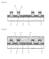
- FIGS. 1 and 2 are views that illustrate an organic light-emitting device according to an exemplary embodiment of the present invention.
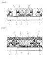
- FIGS. 3 to 6 are views that illustrate a method for preparing an organic light-emitting device according to the exemplary embodiment of the present invention.
- the method for preparing the organic light-emitting device comprises the steps of: 1) forming a spacer pattern 50 on a first electrode 20 formed on a substrate 10; 2) forming an organic material layer 30 and a second electrode 40; 3) exposing the first electrode 20 by forming an encapsulation thin film 60 and then etching at least one portion of the encapsulation thin film 60; and 4) forming an auxiliary electrode 70 which is electrically connected to the first electrode 20 exposed in the exposing of the first electrode 20.
- the present invention provides an organic light-emitting device prepared by the method for preparing organic light-emitting device.
- the organic light-emitting device according to the exemplary embodiment of the present invention may be more preferably applied to an organic light-emitting device for lighting.
- the present invention provides an organic light-emitting device comprising a substrate, a first electrode, an organic material layer, and a second electrode, the organic light-emitting device comprising: a spacer pattern formed on the first electrode, an auxiliary electrode electrically connected to the first electrode; and an encapsulation thin film between the second electrode and the auxiliary electrode.
- the first electrode which is the transparent electrode since the first electrode which is the transparent electrode has low conductivity, a voltage drop occurs due to electrode resistance in a longitudinal direction from a first electrode pad terminal to the center of the diode at the time of implementing the diode having a large area, which causes brightness non-uniformity of the diode.
- the organic light-emitting device may prevent the voltage drop due to the electrode resistance by forming the auxiliary electrode by the specific method, thereby preventing the brightness non-uniformity of the diode.
Landscapes
- Physics & Mathematics (AREA)
- Optics & Photonics (AREA)
- Engineering & Computer Science (AREA)
- Manufacturing & Machinery (AREA)
- Electroluminescent Light Sources (AREA)
Applications Claiming Priority (2)
| Application Number | Priority Date | Filing Date | Title |
|---|---|---|---|
| KR20100065710 | 2010-07-08 | ||
| PCT/KR2011/005013 WO2012005540A2 (fr) | 2010-07-08 | 2011-07-08 | Dispositif électroluminescent organique et son procédé de fabrication |
Publications (3)
| Publication Number | Publication Date |
|---|---|
| EP2592672A2 true EP2592672A2 (fr) | 2013-05-15 |
| EP2592672A4 EP2592672A4 (fr) | 2016-06-22 |
| EP2592672B1 EP2592672B1 (fr) | 2021-01-27 |
Family
ID=45441674
Family Applications (1)
| Application Number | Title | Priority Date | Filing Date |
|---|---|---|---|
| EP11803826.4A Active EP2592672B1 (fr) | 2010-07-08 | 2011-07-08 | Dispositif électroluminescent organique et son procédé de fabrication |
Country Status (6)
| Country | Link |
|---|---|
| US (2) | US9099671B2 (fr) |
| EP (1) | EP2592672B1 (fr) |
| JP (3) | JP2013531345A (fr) |
| KR (1) | KR101367584B1 (fr) |
| CN (1) | CN103081159B (fr) |
| WO (1) | WO2012005540A2 (fr) |
Cited By (1)
| Publication number | Priority date | Publication date | Assignee | Title |
|---|---|---|---|---|
| US11749783B2 (en) | 2018-07-27 | 2023-09-05 | Samsung Display Co., Ltd. | Light emitting device, manufacturing method thereof, and display device having same |
Families Citing this family (11)
| Publication number | Priority date | Publication date | Assignee | Title |
|---|---|---|---|---|
| CN103296052B (zh) * | 2012-02-29 | 2015-11-04 | 群康科技(深圳)有限公司 | 显示面板及显示装置 |
| TWI565115B (zh) | 2012-05-31 | 2017-01-01 | 樂金顯示科技股份有限公司 | 有機發光裝置及其製備方法 |
| WO2015023162A1 (fr) * | 2013-08-16 | 2015-02-19 | 주식회사 엘지화학 | Substrat conducteur et son procédé de fabrication |
| WO2015026185A1 (fr) * | 2013-08-21 | 2015-02-26 | 주식회사 엘지화학 | Dispositif électroluminescent organique et procédé de fabrication correspondant |
| TWI563704B (en) * | 2013-12-31 | 2016-12-21 | Ind Tech Res Inst | Light emitting diode |
| CN104022233B (zh) | 2014-05-28 | 2016-01-06 | 京东方科技集团股份有限公司 | 一种有机发光显示面板的封装方法和有机发光显示面板 |
| KR101579457B1 (ko) * | 2014-12-22 | 2015-12-22 | 코닝정밀소재 주식회사 | 유기발광소자용 광추출 기판 제조방법, 유기발광소자용 광추출 기판 및 이를 포함하는 유기발광소자 |
| KR102598926B1 (ko) * | 2016-10-31 | 2023-11-03 | 엘지디스플레이 주식회사 | 유기발광소자를 이용한 조명장치 및 그 제조방법 |
| CN106784352B (zh) * | 2016-12-28 | 2019-03-29 | 固安翌光科技有限公司 | 有机发光器件及其制造方法 |
| CN108321305B (zh) * | 2018-01-31 | 2020-08-28 | 京东方科技集团股份有限公司 | 一种oled显示面板及显示装置 |
| EP4659553A1 (fr) * | 2023-02-03 | 2025-12-10 | Applied Materials, Inc. | Structure oled et processus basé sur une passivation de pixels par élimination d'une pile oled sur des structures absorbant la chaleur |
Family Cites Families (24)
| Publication number | Priority date | Publication date | Assignee | Title |
|---|---|---|---|---|
| US5294869A (en) * | 1991-12-30 | 1994-03-15 | Eastman Kodak Company | Organic electroluminescent multicolor image display device |
| US5701055A (en) | 1994-03-13 | 1997-12-23 | Pioneer Electronic Corporation | Organic electoluminescent display panel and method for manufacturing the same |
| JP3813217B2 (ja) | 1995-03-13 | 2006-08-23 | パイオニア株式会社 | 有機エレクトロルミネッセンスディスプレイパネルの製造方法 |
| JP3663876B2 (ja) * | 1998-01-08 | 2005-06-22 | 松下電器産業株式会社 | 有機エレクトロルミネセンス素子及びその製造方法 |
| US6630785B1 (en) * | 2000-05-30 | 2003-10-07 | Ritdisplay Corporation | Surface treatment process for fabricating a panel of an organic light emitting device |
| KR100723011B1 (ko) * | 2001-05-28 | 2007-05-29 | 주식회사 동진쎄미켐 | 보조 전극을 갖는 유기 전기발광 디스플레이의 제조 방법 |
| JP4534430B2 (ja) * | 2003-04-24 | 2010-09-01 | セイコーエプソン株式会社 | 電気光学装置、電気光学装置用基板、電気光学装置の製造方法および電子機器 |
| JP3915985B2 (ja) * | 2003-08-22 | 2007-05-16 | セイコーエプソン株式会社 | 画素素子基板、表示装置、電子機器、及び画素素子基板の製造方法 |
| US7052355B2 (en) * | 2003-10-30 | 2006-05-30 | General Electric Company | Organic electro-optic device and method for making the same |
| JP2005158371A (ja) * | 2003-11-25 | 2005-06-16 | Toyota Industries Corp | 有機エレクトロルミネセンス素子とその製造方法、および照明装置 |
| JP4027914B2 (ja) | 2004-05-21 | 2007-12-26 | 株式会社半導体エネルギー研究所 | 照明装置及びそれを用いた機器 |
| US7733441B2 (en) * | 2004-06-03 | 2010-06-08 | Semiconductor Energy Labortory Co., Ltd. | Organic electroluminescent lighting system provided with an insulating layer containing fluorescent material |
| KR100642490B1 (ko) * | 2004-09-16 | 2006-11-02 | 엘지.필립스 엘시디 주식회사 | 유기전계발광 소자 및 그 제조방법 |
| JP2006155920A (ja) * | 2004-11-25 | 2006-06-15 | Denso Corp | El素子の製造方法 |
| JP4367346B2 (ja) * | 2005-01-20 | 2009-11-18 | セイコーエプソン株式会社 | 電気光学装置及びその製造方法、並びに電子機器 |
| JP2007128726A (ja) * | 2005-11-02 | 2007-05-24 | Harison Toshiba Lighting Corp | 有機el発光装置 |
| JP2007234555A (ja) * | 2006-03-03 | 2007-09-13 | Semiconductor Energy Lab Co Ltd | 照明装置 |
| KR101274785B1 (ko) * | 2006-06-30 | 2013-06-13 | 엘지디스플레이 주식회사 | 유기 전계 발광 표시 장치 및 이의 제조 방법 |
| JP2010027210A (ja) | 2008-07-15 | 2010-02-04 | Canon Inc | 有機発光素子の製造方法及び有機発光素子 |
| DE102008049057B4 (de) | 2008-09-26 | 2019-01-31 | Fraunhofer-Gesellschaft zur Förderung der angewandten Forschung e.V. | Organisches opto-elektrisches Bauelement und ein Verfahren zur Herstellung eines organischen opto-elektrischen Bauelements |
| JP5035198B2 (ja) * | 2008-09-26 | 2012-09-26 | 大日本印刷株式会社 | 有機エレクトロルミネッセンス素子およびその製造方法 |
| KR101301180B1 (ko) * | 2008-11-21 | 2013-08-28 | 엘지디스플레이 주식회사 | 듀얼플레이트 방식의 유기전계 발광소자 및 그 합착 방법 |
| JP5748397B2 (ja) * | 2009-07-27 | 2015-07-15 | ローム株式会社 | 有機el装置 |
| JP5010698B2 (ja) | 2010-03-02 | 2012-08-29 | 株式会社東芝 | 照明装置及びその製造方法 |
-
2011
- 2011-07-08 EP EP11803826.4A patent/EP2592672B1/fr active Active
- 2011-07-08 US US13/808,876 patent/US9099671B2/en active Active
- 2011-07-08 JP JP2013518280A patent/JP2013531345A/ja active Pending
- 2011-07-08 CN CN201180042950.5A patent/CN103081159B/zh active Active
- 2011-07-08 WO PCT/KR2011/005013 patent/WO2012005540A2/fr not_active Ceased
- 2011-07-08 KR KR1020110067966A patent/KR101367584B1/ko active Active
-
2015
- 2015-04-22 JP JP2015087383A patent/JP6043401B2/ja active Active
- 2015-04-22 JP JP2015087384A patent/JP6052825B2/ja active Active
- 2015-07-02 US US14/790,883 patent/US10164207B2/en active Active
Cited By (1)
| Publication number | Priority date | Publication date | Assignee | Title |
|---|---|---|---|---|
| US11749783B2 (en) | 2018-07-27 | 2023-09-05 | Samsung Display Co., Ltd. | Light emitting device, manufacturing method thereof, and display device having same |
Also Published As
| Publication number | Publication date |
|---|---|
| JP6043401B2 (ja) | 2016-12-14 |
| CN103081159A (zh) | 2013-05-01 |
| US9099671B2 (en) | 2015-08-04 |
| JP2015156391A (ja) | 2015-08-27 |
| EP2592672B1 (fr) | 2021-01-27 |
| US20150311469A1 (en) | 2015-10-29 |
| EP2592672A4 (fr) | 2016-06-22 |
| US10164207B2 (en) | 2018-12-25 |
| JP6052825B2 (ja) | 2016-12-27 |
| CN103081159B (zh) | 2016-05-25 |
| JP2015156392A (ja) | 2015-08-27 |
| WO2012005540A3 (fr) | 2012-05-31 |
| WO2012005540A2 (fr) | 2012-01-12 |
| KR20120005414A (ko) | 2012-01-16 |
| JP2013531345A (ja) | 2013-08-01 |
| US20130112962A1 (en) | 2013-05-09 |
| KR101367584B1 (ko) | 2014-02-25 |
Similar Documents
| Publication | Publication Date | Title |
|---|---|---|
| EP2592672B1 (fr) | Dispositif électroluminescent organique et son procédé de fabrication | |
| US9035420B2 (en) | Organic light emitting device, display apparatus and illumination apparatus comprising the organic light emitting device, and method for preparing the same | |
| US9740073B2 (en) | Complex display device | |
| KR101882184B1 (ko) | 유기 발광 소자 및 이의 제조방법 | |
| US9966556B2 (en) | Organic light-emitting device having a compensation resistance part electrically connected to the auxiliary electrode | |
| EP3016161B1 (fr) | Dispositif électroluminescent organique | |
| JPWO2017056684A1 (ja) | 有機エレクトロルミネッセンスパネル及びその製造方法 | |
| KR20130135186A (ko) | 플렉서블 전극 및 이의 제조방법 | |
| US9006771B2 (en) | Organic light emitting diode and method for manufacturing the same | |
| KR20130135185A (ko) | 유기 발광 소자 및 이의 제조방법 | |
| EP3018725B1 (fr) | Procédé de fabrication d'un dispositif électroluminescent organique | |
| KR101806940B1 (ko) | 유기 발광 소자 및 이의 제조방법 | |
| KR101677425B1 (ko) | 유기 발광 소자 및 이의 제조방법 | |
| KR20150037025A (ko) | 플렉서블 기판을 포함하는 유기 발광 소자 및 이의 제조방법 |
Legal Events
| Date | Code | Title | Description |
|---|---|---|---|
| PUAI | Public reference made under article 153(3) epc to a published international application that has entered the european phase |
Free format text: ORIGINAL CODE: 0009012 |
|
| 17P | Request for examination filed |
Effective date: 20130108 |
|
| AK | Designated contracting states |
Kind code of ref document: A2 Designated state(s): AL AT BE BG CH CY CZ DE DK EE ES FI FR GB GR HR HU IE IS IT LI LT LU LV MC MK MT NL NO PL PT RO RS SE SI SK SM TR |
|
| DAX | Request for extension of the european patent (deleted) | ||
| RAP1 | Party data changed (applicant data changed or rights of an application transferred) |
Owner name: LG DISPLAY CO., LTD. |
|
| REG | Reference to a national code |
Ref country code: DE Ref legal event code: R079 Ref document number: 602011070066 Country of ref document: DE Free format text: PREVIOUS MAIN CLASS: H01L0051560000 Ipc: H01L0051520000 |
|
| A4 | Supplementary search report drawn up and despatched |
Effective date: 20160525 |
|
| RIC1 | Information provided on ipc code assigned before grant |
Ipc: H01L 51/52 20060101AFI20160519BHEP |
|
| STAA | Information on the status of an ep patent application or granted ep patent |
Free format text: STATUS: EXAMINATION IS IN PROGRESS |
|
| 17Q | First examination report despatched |
Effective date: 20190809 |
|
| GRAP | Despatch of communication of intention to grant a patent |
Free format text: ORIGINAL CODE: EPIDOSNIGR1 |
|
| STAA | Information on the status of an ep patent application or granted ep patent |
Free format text: STATUS: GRANT OF PATENT IS INTENDED |
|
| INTG | Intention to grant announced |
Effective date: 20200924 |
|
| GRAS | Grant fee paid |
Free format text: ORIGINAL CODE: EPIDOSNIGR3 |
|
| GRAA | (expected) grant |
Free format text: ORIGINAL CODE: 0009210 |
|
| STAA | Information on the status of an ep patent application or granted ep patent |
Free format text: STATUS: THE PATENT HAS BEEN GRANTED |
|
| AK | Designated contracting states |
Kind code of ref document: B1 Designated state(s): AL AT BE BG CH CY CZ DE DK EE ES FI FR GB GR HR HU IE IS IT LI LT LU LV MC MK MT NL NO PL PT RO RS SE SI SK SM TR |
|
| REG | Reference to a national code |
Ref country code: GB Ref legal event code: FG4D |
|
| REG | Reference to a national code |
Ref country code: CH Ref legal event code: EP |
|
| REG | Reference to a national code |
Ref country code: AT Ref legal event code: REF Ref document number: 1359149 Country of ref document: AT Kind code of ref document: T Effective date: 20210215 |
|
| REG | Reference to a national code |
Ref country code: IE Ref legal event code: FG4D |
|
| REG | Reference to a national code |
Ref country code: DE Ref legal event code: R096 Ref document number: 602011070066 Country of ref document: DE |
|
| REG | Reference to a national code |
Ref country code: NL Ref legal event code: MP Effective date: 20210127 |
|
| REG | Reference to a national code |
Ref country code: LT Ref legal event code: MG9D |
|
| REG | Reference to a national code |
Ref country code: AT Ref legal event code: MK05 Ref document number: 1359149 Country of ref document: AT Kind code of ref document: T Effective date: 20210127 |
|
| PG25 | Lapsed in a contracting state [announced via postgrant information from national office to epo] |
Ref country code: FI Free format text: LAPSE BECAUSE OF FAILURE TO SUBMIT A TRANSLATION OF THE DESCRIPTION OR TO PAY THE FEE WITHIN THE PRESCRIBED TIME-LIMIT Effective date: 20210127 Ref country code: HR Free format text: LAPSE BECAUSE OF FAILURE TO SUBMIT A TRANSLATION OF THE DESCRIPTION OR TO PAY THE FEE WITHIN THE PRESCRIBED TIME-LIMIT Effective date: 20210127 Ref country code: GR Free format text: LAPSE BECAUSE OF FAILURE TO SUBMIT A TRANSLATION OF THE DESCRIPTION OR TO PAY THE FEE WITHIN THE PRESCRIBED TIME-LIMIT Effective date: 20210428 Ref country code: LT Free format text: LAPSE BECAUSE OF FAILURE TO SUBMIT A TRANSLATION OF THE DESCRIPTION OR TO PAY THE FEE WITHIN THE PRESCRIBED TIME-LIMIT Effective date: 20210127 Ref country code: PT Free format text: LAPSE BECAUSE OF FAILURE TO SUBMIT A TRANSLATION OF THE DESCRIPTION OR TO PAY THE FEE WITHIN THE PRESCRIBED TIME-LIMIT Effective date: 20210527 Ref country code: NO Free format text: LAPSE BECAUSE OF FAILURE TO SUBMIT A TRANSLATION OF THE DESCRIPTION OR TO PAY THE FEE WITHIN THE PRESCRIBED TIME-LIMIT Effective date: 20210427 Ref country code: NL Free format text: LAPSE BECAUSE OF FAILURE TO SUBMIT A TRANSLATION OF THE DESCRIPTION OR TO PAY THE FEE WITHIN THE PRESCRIBED TIME-LIMIT Effective date: 20210127 Ref country code: BG Free format text: LAPSE BECAUSE OF FAILURE TO SUBMIT A TRANSLATION OF THE DESCRIPTION OR TO PAY THE FEE WITHIN THE PRESCRIBED TIME-LIMIT Effective date: 20210427 |
|
| PG25 | Lapsed in a contracting state [announced via postgrant information from national office to epo] |
Ref country code: SE Free format text: LAPSE BECAUSE OF FAILURE TO SUBMIT A TRANSLATION OF THE DESCRIPTION OR TO PAY THE FEE WITHIN THE PRESCRIBED TIME-LIMIT Effective date: 20210127 Ref country code: AT Free format text: LAPSE BECAUSE OF FAILURE TO SUBMIT A TRANSLATION OF THE DESCRIPTION OR TO PAY THE FEE WITHIN THE PRESCRIBED TIME-LIMIT Effective date: 20210127 Ref country code: RS Free format text: LAPSE BECAUSE OF FAILURE TO SUBMIT A TRANSLATION OF THE DESCRIPTION OR TO PAY THE FEE WITHIN THE PRESCRIBED TIME-LIMIT Effective date: 20210127 Ref country code: PL Free format text: LAPSE BECAUSE OF FAILURE TO SUBMIT A TRANSLATION OF THE DESCRIPTION OR TO PAY THE FEE WITHIN THE PRESCRIBED TIME-LIMIT Effective date: 20210127 Ref country code: LV Free format text: LAPSE BECAUSE OF FAILURE TO SUBMIT A TRANSLATION OF THE DESCRIPTION OR TO PAY THE FEE WITHIN THE PRESCRIBED TIME-LIMIT Effective date: 20210127 |
|
| PG25 | Lapsed in a contracting state [announced via postgrant information from national office to epo] |
Ref country code: IS Free format text: LAPSE BECAUSE OF FAILURE TO SUBMIT A TRANSLATION OF THE DESCRIPTION OR TO PAY THE FEE WITHIN THE PRESCRIBED TIME-LIMIT Effective date: 20210527 |
|
| REG | Reference to a national code |
Ref country code: DE Ref legal event code: R097 Ref document number: 602011070066 Country of ref document: DE |
|
| PG25 | Lapsed in a contracting state [announced via postgrant information from national office to epo] |
Ref country code: CZ Free format text: LAPSE BECAUSE OF FAILURE TO SUBMIT A TRANSLATION OF THE DESCRIPTION OR TO PAY THE FEE WITHIN THE PRESCRIBED TIME-LIMIT Effective date: 20210127 Ref country code: EE Free format text: LAPSE BECAUSE OF FAILURE TO SUBMIT A TRANSLATION OF THE DESCRIPTION OR TO PAY THE FEE WITHIN THE PRESCRIBED TIME-LIMIT Effective date: 20210127 Ref country code: SM Free format text: LAPSE BECAUSE OF FAILURE TO SUBMIT A TRANSLATION OF THE DESCRIPTION OR TO PAY THE FEE WITHIN THE PRESCRIBED TIME-LIMIT Effective date: 20210127 |
|
| PG25 | Lapsed in a contracting state [announced via postgrant information from national office to epo] |
Ref country code: RO Free format text: LAPSE BECAUSE OF FAILURE TO SUBMIT A TRANSLATION OF THE DESCRIPTION OR TO PAY THE FEE WITHIN THE PRESCRIBED TIME-LIMIT Effective date: 20210127 Ref country code: SK Free format text: LAPSE BECAUSE OF FAILURE TO SUBMIT A TRANSLATION OF THE DESCRIPTION OR TO PAY THE FEE WITHIN THE PRESCRIBED TIME-LIMIT Effective date: 20210127 Ref country code: ES Free format text: LAPSE BECAUSE OF FAILURE TO SUBMIT A TRANSLATION OF THE DESCRIPTION OR TO PAY THE FEE WITHIN THE PRESCRIBED TIME-LIMIT Effective date: 20210127 Ref country code: DK Free format text: LAPSE BECAUSE OF FAILURE TO SUBMIT A TRANSLATION OF THE DESCRIPTION OR TO PAY THE FEE WITHIN THE PRESCRIBED TIME-LIMIT Effective date: 20210127 |
|
| PLBE | No opposition filed within time limit |
Free format text: ORIGINAL CODE: 0009261 |
|
| STAA | Information on the status of an ep patent application or granted ep patent |
Free format text: STATUS: NO OPPOSITION FILED WITHIN TIME LIMIT |
|
| 26N | No opposition filed |
Effective date: 20211028 |
|
| PG25 | Lapsed in a contracting state [announced via postgrant information from national office to epo] |
Ref country code: AL Free format text: LAPSE BECAUSE OF FAILURE TO SUBMIT A TRANSLATION OF THE DESCRIPTION OR TO PAY THE FEE WITHIN THE PRESCRIBED TIME-LIMIT Effective date: 20210127 |
|
| PG25 | Lapsed in a contracting state [announced via postgrant information from national office to epo] |
Ref country code: SI Free format text: LAPSE BECAUSE OF FAILURE TO SUBMIT A TRANSLATION OF THE DESCRIPTION OR TO PAY THE FEE WITHIN THE PRESCRIBED TIME-LIMIT Effective date: 20210127 |
|
| REG | Reference to a national code |
Ref country code: CH Ref legal event code: PL |
|
| PG25 | Lapsed in a contracting state [announced via postgrant information from national office to epo] |
Ref country code: MC Free format text: LAPSE BECAUSE OF FAILURE TO SUBMIT A TRANSLATION OF THE DESCRIPTION OR TO PAY THE FEE WITHIN THE PRESCRIBED TIME-LIMIT Effective date: 20210127 |
|
| REG | Reference to a national code |
Ref country code: BE Ref legal event code: MM Effective date: 20210731 |
|
| PG25 | Lapsed in a contracting state [announced via postgrant information from national office to epo] |
Ref country code: LI Free format text: LAPSE BECAUSE OF NON-PAYMENT OF DUE FEES Effective date: 20210731 Ref country code: IT Free format text: LAPSE BECAUSE OF FAILURE TO SUBMIT A TRANSLATION OF THE DESCRIPTION OR TO PAY THE FEE WITHIN THE PRESCRIBED TIME-LIMIT Effective date: 20210127 Ref country code: CH Free format text: LAPSE BECAUSE OF NON-PAYMENT OF DUE FEES Effective date: 20210731 |
|
| PG25 | Lapsed in a contracting state [announced via postgrant information from national office to epo] |
Ref country code: IS Free format text: LAPSE BECAUSE OF FAILURE TO SUBMIT A TRANSLATION OF THE DESCRIPTION OR TO PAY THE FEE WITHIN THE PRESCRIBED TIME-LIMIT Effective date: 20210527 Ref country code: LU Free format text: LAPSE BECAUSE OF NON-PAYMENT OF DUE FEES Effective date: 20210708 |
|
| PG25 | Lapsed in a contracting state [announced via postgrant information from national office to epo] |
Ref country code: IE Free format text: LAPSE BECAUSE OF NON-PAYMENT OF DUE FEES Effective date: 20210708 Ref country code: BE Free format text: LAPSE BECAUSE OF NON-PAYMENT OF DUE FEES Effective date: 20210731 |
|
| REG | Reference to a national code |
Ref country code: DE Ref legal event code: R079 Ref document number: 602011070066 Country of ref document: DE Free format text: PREVIOUS MAIN CLASS: H01L0051520000 Ipc: H10K0050800000 |
|
| PG25 | Lapsed in a contracting state [announced via postgrant information from national office to epo] |
Ref country code: HU Free format text: LAPSE BECAUSE OF FAILURE TO SUBMIT A TRANSLATION OF THE DESCRIPTION OR TO PAY THE FEE WITHIN THE PRESCRIBED TIME-LIMIT; INVALID AB INITIO Effective date: 20110708 Ref country code: CY Free format text: LAPSE BECAUSE OF FAILURE TO SUBMIT A TRANSLATION OF THE DESCRIPTION OR TO PAY THE FEE WITHIN THE PRESCRIBED TIME-LIMIT Effective date: 20210127 |
|
| PG25 | Lapsed in a contracting state [announced via postgrant information from national office to epo] |
Ref country code: MK Free format text: LAPSE BECAUSE OF FAILURE TO SUBMIT A TRANSLATION OF THE DESCRIPTION OR TO PAY THE FEE WITHIN THE PRESCRIBED TIME-LIMIT Effective date: 20210127 |
|
| PG25 | Lapsed in a contracting state [announced via postgrant information from national office to epo] |
Ref country code: MT Free format text: LAPSE BECAUSE OF FAILURE TO SUBMIT A TRANSLATION OF THE DESCRIPTION OR TO PAY THE FEE WITHIN THE PRESCRIBED TIME-LIMIT Effective date: 20210127 |
|
| PGFP | Annual fee paid to national office [announced via postgrant information from national office to epo] |
Ref country code: GB Payment date: 20250520 Year of fee payment: 15 |
|
| PGFP | Annual fee paid to national office [announced via postgrant information from national office to epo] |
Ref country code: FR Payment date: 20250521 Year of fee payment: 15 |
|
| PGFP | Annual fee paid to national office [announced via postgrant information from national office to epo] |
Ref country code: DE Payment date: 20250520 Year of fee payment: 15 |
|
| PG25 | Lapsed in a contracting state [announced via postgrant information from national office to epo] |
Ref country code: TR Free format text: LAPSE BECAUSE OF FAILURE TO SUBMIT A TRANSLATION OF THE DESCRIPTION OR TO PAY THE FEE WITHIN THE PRESCRIBED TIME-LIMIT Effective date: 20210127 |