EP2593749B1 - Modulation de différence de phase d'étalonnage par intermittence pour interféromètre de sagnac - Google Patents
Modulation de différence de phase d'étalonnage par intermittence pour interféromètre de sagnac Download PDFInfo
- Publication number
- EP2593749B1 EP2593749B1 EP10854823.1A EP10854823A EP2593749B1 EP 2593749 B1 EP2593749 B1 EP 2593749B1 EP 10854823 A EP10854823 A EP 10854823A EP 2593749 B1 EP2593749 B1 EP 2593749B1
- Authority
- EP
- European Patent Office
- Prior art keywords
- phase
- modulation
- difference
- calibration
- waveform
- Prior art date
- Legal status (The legal status is an assumption and is not a legal conclusion. Google has not performed a legal analysis and makes no representation as to the accuracy of the status listed.)
- Not-in-force
Links
- 230000003287 optical effect Effects 0.000 claims description 54
- 238000000034 method Methods 0.000 claims description 41
- 239000000835 fiber Substances 0.000 claims description 28
- 230000007704 transition Effects 0.000 claims description 22
- 230000004913 activation Effects 0.000 claims 3
- 230000003213 activating effect Effects 0.000 claims 1
- 230000009849 deactivation Effects 0.000 claims 1
- 238000013459 approach Methods 0.000 description 56
- 238000012545 processing Methods 0.000 description 31
- 230000006870 function Effects 0.000 description 30
- 238000005259 measurement Methods 0.000 description 29
- 230000009977 dual effect Effects 0.000 description 24
- 238000006243 chemical reaction Methods 0.000 description 20
- 238000012546 transfer Methods 0.000 description 17
- 238000010586 diagram Methods 0.000 description 15
- 230000010363 phase shift Effects 0.000 description 12
- 230000035945 sensitivity Effects 0.000 description 11
- 238000013461 design Methods 0.000 description 9
- 230000008859 change Effects 0.000 description 7
- 239000013307 optical fiber Substances 0.000 description 6
- 238000005070 sampling Methods 0.000 description 6
- 230000000694 effects Effects 0.000 description 5
- 238000001914 filtration Methods 0.000 description 5
- 230000002452 interceptive effect Effects 0.000 description 5
- 230000008569 process Effects 0.000 description 5
- 230000001902 propagating effect Effects 0.000 description 5
- 230000035508 accumulation Effects 0.000 description 4
- 238000009825 accumulation Methods 0.000 description 4
- 238000010606 normalization Methods 0.000 description 4
- 230000004044 response Effects 0.000 description 4
- 230000007774 longterm Effects 0.000 description 3
- 230000004048 modification Effects 0.000 description 3
- 238000012986 modification Methods 0.000 description 3
- 230000001360 synchronised effect Effects 0.000 description 3
- 230000001419 dependent effect Effects 0.000 description 2
- 230000007613 environmental effect Effects 0.000 description 2
- 230000006872 improvement Effects 0.000 description 2
- 230000010287 polarization Effects 0.000 description 2
- 230000009466 transformation Effects 0.000 description 2
- 238000012935 Averaging Methods 0.000 description 1
- ATJFFYVFTNAWJD-UHFFFAOYSA-N Tin Chemical compound [Sn] ATJFFYVFTNAWJD-UHFFFAOYSA-N 0.000 description 1
- 230000001133 acceleration Effects 0.000 description 1
- 230000009471 action Effects 0.000 description 1
- 230000002411 adverse Effects 0.000 description 1
- 230000001934 delay Effects 0.000 description 1
- 238000003384 imaging method Methods 0.000 description 1
- 238000000691 measurement method Methods 0.000 description 1
- 230000008520 organization Effects 0.000 description 1
- 230000000737 periodic effect Effects 0.000 description 1
- 238000002360 preparation method Methods 0.000 description 1
- 238000005215 recombination Methods 0.000 description 1
- 230000006798 recombination Effects 0.000 description 1
- 230000002441 reversible effect Effects 0.000 description 1
- 238000011105 stabilization Methods 0.000 description 1
- 230000001131 transforming effect Effects 0.000 description 1
Images








Classifications
-
- G—PHYSICS
- G01—MEASURING; TESTING
- G01C—MEASURING DISTANCES, LEVELS OR BEARINGS; SURVEYING; NAVIGATION; GYROSCOPIC INSTRUMENTS; PHOTOGRAMMETRY OR VIDEOGRAMMETRY
- G01C19/00—Gyroscopes; Turn-sensitive devices using vibrating masses; Turn-sensitive devices without moving masses; Measuring angular rate using gyroscopic effects
- G01C19/58—Turn-sensitive devices without moving masses
- G01C19/64—Gyrometers using the Sagnac effect, i.e. rotation-induced shifts between counter-rotating electromagnetic beams
- G01C19/72—Gyrometers using the Sagnac effect, i.e. rotation-induced shifts between counter-rotating electromagnetic beams with counter-rotating light beams in a passive ring, e.g. fibre laser gyrometers
- G01C19/726—Phase nulling gyrometers, i.e. compensating the Sagnac phase shift in a closed loop system
Definitions
- the present invention relates, in general, to gyroscopes and, more particularly, to closed-loop fiber optic gyroscopes and, even more particularly, closed-loop fiber optic gyroscopes using a Sagnac interferometer.
- a Sagnac interferometer comprises a splitting plate or other splitting device that divides an incident light wave into two lightwaves.
- the two waves thus created enter opposite ends of a single optical path formed into a loop.
- the two waves counter-propagate, pass through each other, and return to the splitting device. There they recombine and are sent to a detector where they produce interference that depends upon phase difference between the recombined waves.
- mirrors defined the optical path of the Sagnac interferometers. It is now known that this optical path can be created using a single-mode optical fiber wound about an axis into a coil.
- a constant frequency offset is equivalent to a constant rate-of-change in phase, or, in other words, a ramp in phase vs. time with a constant slope.
- a phase modulator can generate a phase ramp for a short period of time, but it then reaches the limit of its capability.
- An instantaneous 2 ⁇ shift in the phase is transparent to an optical wave, and therefore a serrodyne waveform, consisting of a ramp and fall-back, created by a phase modulator appears like a continuous phase ramp and therefore also like a frequency shift.
- the aforesaid second control loop has been implemented in different ways. All of these have in effect rendered the actual ratio of the phase modulation output to electronic input, i.e. the phase modulator transfer function, non-critical to the measurement of Sagnac phase difference.
- the second control loop calibrates the phase modulator transfer function against the response of the interferometer. If the second control loop works well, then the measurement becomes as good as the interferometer response, and therefore as good as fundamental parameters such as wavelength stability and fiber coil stability.
- the signal following the fall back is used as the input to the second control loop. This signal indicates an error if the fall back differs from 2 ⁇ radians, and thus it calibrates the phase modulator transfer function with respect to the optical signal.
- the detector output is digitized, signal processed, and converted back into an analog waveform to drive the phase modulator.
- the electronic signal processing may comprise a combination of analog signal-conditioning electronics, conversion electronics, and digital electronics. With this arrangement it is easier to change the level of the electronic drive waveform in discrete steps rather than continuously.
- phase modulation steps can provide a similar phase difference between the recombined counter-propagated waves as a continuous ramp. The continuous ramp and fall-back then becomes a series of steps and a fall-back. See, for example, U.S. Pats. No. 5,039,220 , 5,141,316 , 5,181,078 .
- a fiber-optic gyroscope 1 includes a quasi-monochromatic light source 15, that is most often a super-luminescent diode or a laser diode pumped erbium-doped optical fiber, and a single-mode fiber optic Sagnac loop interferometer, designated overall by the reference 10.
- the Sagnac loop interferometer 10 comprises a first beam splitter 19 and an optical path 20 constituted by a single-mode optical fiber wound into a coil.
- the incident light wave is divided into two waves by the beam splitter.
- the two waves thus created are fed into opposite ends of the optical fiber and propagate in opposite directions, or counter-propagate, through the fiber.
- the counter-propagating waves pass through each other and return to the beam splitter where they are each split again thereby creating four waves. Two of these four waves, a portion from each of the counter-propagated waves, combine with each other and return in the direction of the source of the incident wave while the other two combine with each other but exit the interferometer through the unused port of the first beam splitter 19 and are discarded.
- phase modulator 14 that, controlled on the basis of an electrical signal, imparts a phase shift ⁇ m ( t ) to both of the counter-propagating waves.
- Phase modulation, ⁇ m ( t ) is distinguished from phase difference modulation, ⁇ m ( t ), in the discussion that follows.
- Phase modulation, ⁇ m ( t ), is added to the phase of each of the counter-propagating waves at the phase modulator 14.
- Phase difference modulation, ⁇ m ( t ) is the modulation of the difference between the phases of the two waves as they interfere with each other at the detector 11.
- the detected optical power is largely dependent upon the total phase difference, ⁇ T ( t ), between the interfering waves.
- the total phase difference is ideally the sum of the modulated phase difference plus the rotation-rate induced phase difference.
- the operation of the interferometer is improved by interposing a polarizer 17 and a spatial filter 18 between the second beam splitter 16 and the first beam splitter 19.
- this spatial filter is constituted by a single-mode optical fiber.
- Light returning from the interferometer 10 must have a component of its polarization aligned with pass axis of the polarizer 17.
- Employing polarization-maintaining fiber with its axes of birefringence properly aligned will ensure that some light is passed by the polarizer 17 and delivered to the detector 11.
- the pass axis of the polarizer 17 is vertical, and the slow axis of each of the fiber ends is vertical, and the first beam splitter 19 is relatively insensitive to the polarization of the light, or its birefringence axis is similarly aligned, then a large amount of the light returning to the polarizer 17 will pass through to the second beam splitter 16 and on to the detector 11.
- the output of the detector 11 is prepared and digitized with an analog-to-digital converter 12.
- the proper signal preparation necessary to avoid excess errors in the digital conversion is described in the next subsection.
- Closed-loop signal processing and digital-to-analog conversion electronics herein referred to as signal processor 13, provides negative feedback to control the phase modulator 14 as a function of the signal received from the detector 11. It also creates the bias modulation that is added to the feedback modulation. Finally it derives the rotation rate measurement value that is output for external use.
- FIG. 3 A block diagram of analog-to-digital conversion electronics 12 of FIG.1 is shown in FIG. 3 .
- the output of the detector 11 passes through an amplifier 21 and a low-pass filter 22 before reaching the analog-to digital converter (ADC) 23.
- ADC analog-to digital converter
- Analog-to-digital conversion changes an electronic signal and electronic noise that accompanies the signal, but this change can be made to have almost negligible impact in the signal-to-noise ratio if three criteria are met.
- the first criterion is that the noise accompanying the analog signal must have a standard deviation that is larger than about one least significant bit (LSB) of the ADC 23.
- the amplifier 21 is used to increase both signal and noise that is output from the detector 11 to satisfy the first criterion.
- the second criterion is that the dynamic range of the signal and noise are smaller that the dynamic range of the ADC 23. Thus the amplifier is not allowed to over-amplify the signal and noise, and the ADC must have enough bits to measure the signal plus noise.
- the third criterion is that the low-pass filter 22 must attenuate the analog frequency components that are approximately equal to or greater than the sampling frequency of the ADC 23. These components are undesirable because high frequency analog noise can alias to low frequency digital noise by the digitization process.
- the Shannon criterion therefore imposes a large pass band on the signal to be sampled: it has to be equal to 1/(2 times the sampling period), namely 1.6 MHz in this example.
- the noise is relatively large: typically a standard deviation of 10 -3 of the detected optical power, which corresponds to a phase shift of about 10 -3 radians in the interferometer.
- the LSB correspond to this phase shift.
- the high limit must be at least greater than the peak-to-peak value of the noise, namely about 8 times its standard deviation and hence 3 bits would suffice for sampling the noise alone.
- account must also be taken of the inherent variations in the signal: in closed-loop mode the latter is slaved to zero and would not therefore a priori lay claim to any variations but in practice the slaving deviates from zero during changes in the rotation rate, i.e. angular acceleration, and the dynamic range of the converter must be able to cope with these deviations. These variations therefore define the number of necessary bits. In practice 8 to 12 bits are sufficient at the converter level, whilst after digital filtering the dynamic range of the rotation rate measurement can be greater than 20 bits.
- the staircase-and-fall-back approach has a first control loop to null the Sagnac phase difference and a second control loop to control the gain of the digital-to-analog conversion and phase modulation portions of the first control loop.
- I will refer to the first control loop of this approach as the rotation-rate control loop because it is responsive to the rotation rate.
- I will refer to the second control loop as the calibration control loop because it calibrates the digital values in the signal processing against the phase modulation of the optical wave.
- the prior-art dual staircase approach also has two control loops, a first control loop to control the height of the up-steps to shift the total phase difference to plus ⁇ radians and a second to control the down steps to shift the total phase difference to minus ⁇ radians.
- the up-step height is not the same as the down-step height. Therefore there is a difference between the number of up steps and the number of down steps and this difference is used as a measure of rotation.
- the rotation rate measurement in both the dual-staircase approach and the staircase-and-fall-back approach is largely independent of the phase modulator transfer function.
- the signals involved in the above-mentioned control loops share the same path through most of the gyroscope. Their paths differ only within the closed loop signal processing and the digital-to-analog conversion electronics.
- To trace the common paths one can begin at the phase modulator 14, progress through the optics, through the detector 11, and through the analog-to-digital conversion electronics 12.
- the latter comprises the amplifier 21, the low-pass filter 22, and the ADC 23.
- the completion of the individual paths through the signal processing and through the digital-to-analog conversion electronics is discussed in detail in US patent number 7,505,139, issued March 17, 2009, to Bergh , the inventor here.
- the dual-staircase sections of the waveform occur one after another.
- the prior art approach has led to an unacceptable amount of measurement error in some gyroscopes.
- the present disclosure provides a new and novel process to accomplish this calibration task using an occasional dual-staircase waveform where two steps or more are taken in one direction and then two steps or more are taken in the other.
- An occasional calibration waveform is used to, first, make an interferometer sensitive to small changes in Sagnac phase difference due to rotating the gyroscope (this is commonly referred to as biasing the interferometer); second, supply a feedback phase difference to keep the interferometer sensitive to small changes in rotation rate; and third, supply the calibration modulation necessary to keep the digital electronics calibrated with respect to the Sagnac phase difference being measured.
- Example embodiments are described herein with respect to fiber optic gyroscopes. Methods and systems in accordance with several example embodiments of the invention as defined in the appended claims may not include all of the features shown in these figures. Throughout the figures, like reference numbers refer to similar or identical components or procedures.
- phase modulator 14 begins by reiterating how phase modulation applied to two counter-propagating waves within a Sagnac interferometer by phase modulator 14 (see FIG. 1 ) becomes phase difference modulation between the two waves as they exit the interferometer and interfere with each other at the detector.
- the seemingly complex phase modulation and phase-difference modulation is described as a sum of three or four relatively simple phase modulation components and phase-difference modulation components, respectively.
- Digital signal modulations present within the signal processing correspond directly to both phase modulation and to phase difference modulations. Understanding this correspondence will also make it easier to understand the signal processing as set forth herein.
- phase modulation and the symbol “ ⁇ m ( t )” are reserved for the modulation applied to both of the counter-propagating waves at the phase modulator 14 and the terms “phase difference,” and “phase difference modulation,” and the symbol “ ⁇ ( t )” are used in reference to the difference between the phases of the counter-propagating waves as they interfere with each other at the detector.
- the two counter propagating waves are derived from a single light wave.
- any phase difference at the detector is due to the relative length of their optical paths as they propagate in opposite directions around the fiber loop. Their differences are ideally due to the rotation rate of the interferometer and phase difference modulation.
- the phase modulation creates phase difference modulation because the phase modulator is not at the center of the fiber loop.
- phase modulator In fact it is typically positioned at one end of the fiber loop.
- a first light wave propagating in one direction passes through the phase modulator just before it leaves the interferometer and it reaches the detector almost immediately thereafter.
- a second light wave propagating in the opposite direction passes through the phase modulator and then through the fiber loop. Phase modulation applied equally to both waves is not equal for the two waves interfering at the detector.
- ⁇ is the optical wave propagation time difference between the short and long paths from phase modulator 14 to detector 11.
- the Sagnac interferometer together with the off-center phase modulator 14 converts phase modulation at the phase modulator 14 into phase difference modulation at the detector 11 according to the above formula.
- the feedback accumulator 30 does the reverse.
- a digital signal modulation that corresponds to phase difference modulation at the input of the feedback accumulator 30 is converted into a digital signal modulation that corresponds to phase modulation at its output.
- the output digital signal modulation is converted to an analog electrical signal that drives the phase modulator.
- the phase modulation might then be considered an intermediate stage between digital signal modulation corresponding to phase difference modulation and actual phase difference modulation. This correspondence between the digital signal modulation at the input of the feedback accumulator 30 and the phase difference modulation will make it easier to understand the signal processing block diagram in FIG. 4
- the phase modulation is designed to accomplish four major tasks simultaneously, and can be understood as the sum of four separate component modulations.
- First of these four is a bias modulation that enables electronics to create a demodulated error signal that is linearly related to any small additional phase differences.
- Second is a first feedback phase modulation that compensates for phase difference due to rotation. This compensation is imperfect in the short term, but by keeping the phase difference small to maintain the linear relationship, any error is not lost and the error can be compensated for in the long term.
- a third component keeps the phase modulation from exceeding dynamic range of the phase modulator 14, and a fourth component is a second feedback phase modulation that calibrates digital values within the signal processing in terms of phase modulation of the optical waves within the interferometer. Improving this fourth component of modulation is one of the purposes of this invention.
- the fundamental frequency of the bias modulation is matched to the phase modulator position in the Sagnac interferometer such that its period is 2 ⁇ then regardless of the shape of the bias phase modulation waveform, it transforms to a bias phase difference modulation that oscillates symmetrically about zero. Therefore when the bias phase difference modulation is added to another phase difference, then the total phase difference oscillates back and forth symmetrically about the preexisting phase difference.
- the bias phase modulation of the preferred embodiment of the present invention is a square wave with period 2 ⁇ and peak-to-peak amplitude ⁇ /2. This becomes a square wave bias phase-difference modulation with the same 2 ⁇ period, but with peak-to-peak amplitude of ⁇ .
- a small phase difference, ⁇ ⁇ is shifted with bias phase difference modulation alternately to ⁇ ⁇ ⁇ ⁇ + ⁇ 2 for duration ⁇ and to ⁇ ⁇ ⁇ ⁇ - ⁇ 2 for duration ⁇ .
- the detected optical power is sensitive to small changes in the small phase difference ⁇ ⁇ . This sensitivity to small changes in phase difference will not exist without the bias modulation.
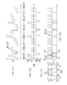
- the detected optical power is the same for all odd integer multiples of ⁇ /2 radians of phase difference. Therefore, while the phase difference is shifting by large amounts, from say minus 3 ⁇ /2 to minus ⁇ /2 to ⁇ /2 to 3 ⁇ /2, the detected optical power remains constant except for spikes in optical power that occur during the transitions from one phase difference value to another, see FIG. 12 .
- the amplitude of the bias modulation is selected above to be ⁇ /2, but this value is not necessary. Any value between 0 and ⁇ will work, and there are good reasons for selecting values other than ⁇ /2 to optimize one characteristic or another.
- the detected optical power can be reduced by adjusting the bias modulation amplitude, and this reduces some noise terms to a larger extent than it reduces the signal.
- the rotation-rate feedback loop introduces a rotation-rate feedback phase-difference modulation (RRFPDM), ⁇ mR ( t ) or 802 in FIGS. 6B , 6C , 9B , 9C , 10B , and 11B that is intended to be equal-and-opposite to the phase difference due to rotation, i.e. the Sagnac phase difference, ⁇ R ( t ).
- the rotation rate loop attempts to null the sum of these two phase-differences. If the rotation rate changes in time, then the Sagnac phase difference, ⁇ R ( t ), changes, and an error signal becomes nonzero.
- the RRFPDM ⁇ mR ( t ) 802 is adjusted in order to zero the error signal, and thereby become once again equal to the Sagnac phase difference, ⁇ ⁇ R ( t ).
- the RRFPDM ⁇ ⁇ mR ( t ) 802 is thereby proportional to the rotation rate, and the digital value used to create it is also proportional to the rotation rate.
- the nulling process is less than perfect in the short term. It is influenced by noise from a variety of sources; a finite closed loop bandwidth combined with a rate of change of rotation rate; and limited digital resolution of DAC 31 (see FIG. 4 .). Deviations from null are not lost, and in time the averaged value of the sum of the two phase difference components is very accurately zeroed.
- the calibration control loop either measures or imposes a relationship between a digital value in the signal processor and a corresponding phase difference between the two waves exiting the interferometer. This relationship can be described as a transfer function.
- This transfer function in a well-designed FOG is largely independent of frequency and thus can be assumed to be a constant of proportionality.
- the value of the proportionality constant is dependent upon a variety of parameters, not the least of which is temperature. As a result, the constant must be measured frequently so that the appropriate value is used to properly scale the RRFPDMDS.
- a calibration feedback phase-difference modulation digital signal (CFPDMDS) is created and it in turn creates a calibration feedback phase-difference modulation (CFPDM) (see 807 in FIG. 9B and 9C , 809 in FIG. 10B , and 811 in FIG. 11B ) that is adjusted according to the interferogram (see FIG. 2 ) to have a predetermined phase-difference modulation amplitude.
- a digital signal is created that represents a phase difference of 2 ⁇ radians and this digital signal can be referred to as a 2 ⁇ digital signal (2 ⁇ DS). If the measurement technique is used, then each time this transfer function is measured, the 2 ⁇ DS is updated.
- Both the RRFPDMDS and the 2 ⁇ DS depend in the same way upon the transfer function and by dividing the RRFPDMDS by the 2 ⁇ DS (see divider 40 in FIG. 4 ) the transfer function is eliminated from the rotation-rate measurement. Another technique stabilizes the transfer function. Both techniques perform a real time calibration of the signal processing with respect to the phase differences affecting the interferogram. As a result of updating the 2 ⁇ DS in real time using the calibration control loop an accurate measure of rotation rate can be made even in a time varying environment.
- the calibration control loop is implemented differently between the present invention and the two prior art approaches: the staircase-and-fall-back approach and the prior art dual-staircase approach of the '139 patent.
- These two prior art approaches had to be modified to be able to be combined to make the occasional calibration approach.
- the transfer function between digital values and the actual phase modulation is measured to create the 2 ⁇ DS and then the RRFPDMDS is divided by the 2 ⁇ DS to remove any variations in the transfer function.
- the transfer function is stabilized so that a fixed value within the digital signal processing always represents a fixed phase difference. Both the measurement-and-normalization approach and the transfer-function-stabilization approach are valid techniques to effect calibration.
- the prior art staircase-and-fall-back was modified to create a new staircase-and-fall-back approach that used the measurement-and-normalization technique in order to make it work with the dual-staircase approach.
- the prior art dual-staircase approach of the '139 patent had a calibration modulation that switched back and forth between plus ⁇ and minus ⁇ (see 803 in FIG. 6B ).
- This calibration phase-difference modulation had to be changed to switch between plus 2 ⁇ , minus 2 ⁇ and zero (see 807 in FIGS. 9B and 9C ). This was necessary in order to set the calibration phase-difference modulation to zero for periods of time. This is a fundamental part of the occasional calibration technique.
- the calibration component of the phase modulation in its simplest form switches between two values: a first substantially constant value and a second substantially constant value that is controlled to be on average 2 ⁇ greater than the first value (see 707 in FIG. 9A ).
- Another embodiment also includes a third substantially constant value that is controlled to be on average 2 ⁇ less than the first value (see 711 in FIG. 11A ).
- the new calibration modulation can still result in a dual-staircase modulation waveform when combined correctly with the bias modulation as shall be seen in the section on waveforms below.
- FIG. 4 A block diagram of the electronics for the occasional calibration is shown in FIG. 4 .
- a specified phase difference value e.g. 2 ⁇
- the digital value corresponding to the phase difference needed to null the rotation-rate phase difference is noted and the latter is normalized by dividing by the former in order to determine the actual phase difference.
- the denominator changes a small amount with the environment. This is primarily because the transfer function of the phase modulator changes with the environment. Thus the normalization must be done in real time to remove environmental effects. Environmental changes occur slowly and the calibration feedback loop does not need to be fast to keep up. For example, it is sufficient to make the calibration measurement at a rate of 10 kHz or less.
- the prior art dual-staircase technique makes calibration measurements at a rate on the order of 100 kHz depending on the length of fiber in the fiber coil.
- the present invention significantly improves the calibration feedback control loop over what is available in the prior art.
- the calibration control loop of the present invention provides a feedback signal that is relatively independent of rotation-rate because it makes measurements at times that are substantially different from the waveform adjustment transitions.
- the calibration feedback of the staircase and fallback technique relies upon the fallback portion of the waveform to obtain the information to close the loop.
- the frequency of the fallbacks is proportional to the rate of rotation.
- the error signal for loop closure and likewise the gain of the feedback loop are proportional to the rotation rate. This type of feedback loop is less than ideal.
- the calibration feedback of the dual-staircase technique is largely independent of rotation rate, and this is good, but it has the problem that it contributes to an unacceptable bias error to the rotation rate measurement in some fiber optic gyroscopes (FOGs).
- the calibration modulation of the present invention significantly reduces this error.
- the calibration modulation of the present invention contributes a negligible bias measurement error.
- FIG. 4 shows the paths of control signals of the two major control loops, i.e. the rotation rate loop and the calibration loop by way of heavy dark lines. They are common through part of the electronics; specifically from adder 29; through feedback accumulator 30; through digital-to-analog converter (DAC) 31; and amplifier 32 and on to the phase modulator 14.
- the paths of the control loops differ in the beginning of the signal processing electronics.
- the output from ADC 23 is provided as an input to rotation rate signal processor 64 and calibration signal processor 65.
- the output signal of rotation rate signal processor 64 is provided as a first input to signal adder 29, a first input of signal divider 40, and a fist input to limit detector 38.
- the output signal of calibration signal processor 65 is a first input of signal calibration modulator 36 and its output is provided as a second input to signal adder 29 by way of signal adder 37.
- the output signal of calibration signal processor 65 is also the second input of signal divider 40.
- the output of signal divider 40 is provided as the input to measurement output signal electronics 41.
- the output of signal adder 29 is provided as the input to feedback accumulator 30.
- phase modulation digital signal (PMDS) As a second input to limit detector 38 is the output of feedback accumulator 30.
- the RRFPDMDS is produced at the output of the rotation-rate signal processor 64.
- the RRFPDMDS as discussed above is proportional to the rotation rate.
- the calibration signal processor 65 produces at its output a digital value corresponding to an optical phase difference of 2 ⁇ radians, herein identified as the "2 ⁇ digital signal" (2 ⁇ DS).
- the calibration modulator 36 produces at its output digital values corresponding to phase differences of 2 ⁇ , minus 2 ⁇ , and zero (807, 809, and 811).
- the 2 ⁇ and -2 ⁇ values are held for a duration of ⁇ , and the zero value is held for one or more ⁇ .
- the output of the limit detector 38 having as inputs (i) the RRFPDMDS, and (ii) the PMDS (701, 708, and 710) output of the feedback accumulator 30, is a single bit received by the calibration modulator 36.
- the output of the bias generator 39 is added to the CFPDMDSs in adder 37, and its output is added to the rotation-rate digital value in adder 29.
- bias generator 39 also shown in FIG. 4 are bias generator 39 and divider 40.
- the 2 ⁇ DS may be used as an input signal to the bias generator 39, but it is not necessary for accurate rotation-rate measurements.
- Divider 40 having as inputs (i) the RRFPDMDS, and (ii) the 2 ⁇ DS, provides an output signal indicative of the measurement of rotation rate that is received by the measurement output 41 and it is made available for external use.
- the signal enters the block diagram from the analog-to-digital conversion electronics 12 in FIG. 1 , or more particularly from ADC 23 in a detailed block diagram of those electronics in FIG. 3 . It is simultaneously processed in both the rotation-rate signal processor 64 and the calibration signal processor 65.
- the output of the rotation-rate signal processor 64 is the RRFPDMDS.
- the RRFPDMDS is proportional to the Sagnac phase difference.
- the output of the calibration signal processor 65 in the dual staircase implementation is the 2 ⁇ DS.
- the 2 ⁇ DS corresponds to a phase difference between two light waves of 2 ⁇ radians.
- ADC analog-to-digital converter
- amplifier 32 the phase modulator 14
- the present disclosure provides an improved calibration modulator that has a different output in the present invention than it had in the prior art.
- the calibration modulator 36 served to change the sign of a ⁇ digital signal in order to derive a signal that switches from plus to minus the ⁇ digital signal. See FIG. 6B signal 803.
- This modulated ⁇ digital signal became the phase-difference modulation, i.e. plus and minus ⁇ radians, of the calibration control loop.
- a simple prior art calibration modulator 36 is shown in FIG. 5 .
- the current invention provides an occasional calibration modulator 36As shown in FIG. 8 that has the ability to output the three values corresponding to phase differences of 2 ⁇ , -2 ⁇ and zero. See signal 807 in FIGS. 9B and 9C and signal 809 in FIG. 10B and signal 811 in FIG. 11B .
- the values corresponding to 2 ⁇ and -2 ⁇ are each held for one ⁇ before switching to another value.
- the value of zero is held for one ⁇ or many ⁇ .
- the minus 2 ⁇ of the calibration modulation occurs at the same time as the plus ⁇ /2 of the bias modulation.
- a first sequence occurs in one or multiple time periods of 2 ⁇ where the calibration modulation will assume the value of zero for duration ⁇ followed by a value of 2 ⁇ for a duration of ⁇ .
- a second sequence occurs in one or multiple time periods of 2 ⁇ where the calibration modulation will assume the value of minus 2 ⁇ for duration ⁇ followed by a value of zero for a duration of ⁇ .
- a third sequence occurs in one or multiple time periods of ⁇ where the calibration modulation will assume the value of zero for duration ⁇ .
- a typical calibration modulation total sequence might consist of a single first sequence followed by a single second sequence followed by one hundred third sequences.
- Feedback accumulator 30 performs an accumulation, i.e. it adds its input to its output to derive a new output, once per time period ⁇ .
- the time between accumulations is chosen to match the difference in propagation time ⁇ from phase modulator 14 to detector 11 for the two counter-propagating light waves. If the times are well matched, then transforming from phase modulation 708 to phase-difference modulation 808 will compensate for the transformation through the feedback accumulator 30. Accordingly, the input to the feedback accumulator corresponds to the phase-difference modulation 808.
- phase modulation 708 The output of the feedback accumulator is proportional to the phase modulation 708.
- This phase modulation can be described in terms of steps.
- a combination of a transition and an immediately following constant value is referred to as a phase-modulation step; and a phase-modulation up-step is any transition and constant value wherein said transition is from a lesser constant value to a greater constant value, and a phase-modulation down-step comprises a transition and constant value wherein said transition is from a greater value to a lesser value.
- the phase modulation is a combination of sequences including a first sequence comprising a plurality of up-steps one after another; and a second sequence comprising a plurality of down-steps one after another; and a third sequence of alternating between up-steps and down-steps (see 708 in FIG. 10A ).
- the 2 ⁇ portion of the CFPDMDS (and phase difference) is added to the minus ⁇ /2 portion of the bias modulation digital value (and phase difference) to create a plus 3 ⁇ /2 portion of the digital value input to the feedback accumulator 30 (and the phase difference on the interferogram FIG. 2 ).
- the feedback accumulator 30 creates the large up step of the dual staircase modulation from this portion of its input.
- the minus 2 ⁇ portion of the CFPDMDS (and phase difference) is added to the plus ⁇ /2 portion of the bias modulation digital value (and phase difference) to create a minus 3 ⁇ /2 portion of the digital value input to the feedback accumulator 30 (and the phase difference on the interferogram FIG.
- the calibration modulation can be turned on (containing sequences of zero and 2 ⁇ and sequences of minus 2 ⁇ and zero) and off (set to zero) without upsetting either the rotation-rate feedback loop or the calibration feedback loop.
- the calibration feedback loop will not be updated during the sequences while the calibration modulation is set to zero, but this feedback loop is not required to be fast. It is very slow compared to the rotation rate feedback loop. As a result, it does not need to be updated as often as the rotation rate feedback loop. Turning the calibration feedback loop off for extended periods of time reduces errors that are created by it in some FOGs.
- FIG. 4 there shown is a block diagram including the rotation-rate signal processor 64 and calibration signal processor 65, along with the rest of the closed loop signal processing and digital-to-analog conversion electronics 13.
- the rotation-rate signal processor 64 and the calibration signal processor 65 are similar with differing functions, of course. They both perform demodulation with demodulators to obtain an error signal, digital filtering to remove unwanted high frequency signals from the error signals, and accumulation to complete the control loop and obtain a desired digital value corresponding to a particular phase difference. Demodulation distinguishes the rotation-rate error signal from the calibration error signal.
- Each of the aforesaid demodulators samples the output from the ADC 23 and is multiplied by a reference signal.
- the signal is filtered after demodulation, and to explain the filter operation it is helpful to look more closely at the signals entering the demodulators.
- the signal from detector 11 ( FIG. 1 ) is proportional to the detected optical power. It is amplified, filtered, and sampled by the ADC 23 during the flat portion of each phase step.
- the phase difference values are the same for the prior art dual-staircase modulation approach and the current invention occasional calibration approach. Indeed the occasional calibration approach makes use of dual-staircase modulation on occasion.
- the occasional calibration waveform dual-staircase scheme strives to use four values of phase difference. These correspond to two values of bias phase-difference modulation, e.g.
- the error signal from one phase difference step is compensated for by error signals of future phase difference steps so that over time average of the actual phase difference values becomes increasingly close to the desired value of phase difference.
- averaging a signal related to the detected optical power during any given phase difference step is recorded.
- ⁇ 1 signal x1 is obtained and likewise for ⁇ 2 , ⁇ 3 , and ⁇ 4 signals x2, x3, and x4, are obtained, respectively.
- There is at least one new ⁇ ⁇ 1 for every dual-staircase cycle, and each one is slightly different. For simplicity one may use a single constant phase difference to identify them.
- the many corresponding signal values are all identified as x1 . This is likewise true for ⁇ 2 , ⁇ 3 , ⁇ 4 and x2, x3, and x4.
- Error signals are derived from these signals for each control loop.
- an error formed by x1 - x2 can be used to record deviations from the phase difference ⁇ radians.
- the average deviation from ⁇ radians can be reduced by accumulating many pairs of x1 - x2 error signal in an accumulator and adjusting the values of ⁇ 1 and ⁇ 2 . This is what was done in the prior art dual-staircase approach and in the occasional calibration approach. Two main reasons why this phase difference error signal is nonzero are an incorrect RRFPDMDS for the current rotation rate or an incorrect 2 ⁇ DS.
- the error signal formed by x3-x4 used to record deviations from minus ⁇ radians will have the same error. If the RRFPDMDS is correct and 2 ⁇ DS is incorrect then the error signal formed by x3-x4 will have the opposite error, i.e. the same magnitude error but with opposite sign. Using the appropriate filter one can distinguish that the two control loops are separated. In the occasional calibration dual staircase phase modulation approach disclosed herein, the additional error signal formed by x1-x4 is used to update the RRFPDMDS.
- the output of the calibration modulation filter 34 is x1-x2 minus x3-x4.
- the average of this filtered calibration error signal is zeroed by the calibration control loop by adjusting the amplitude of the 2 ⁇ DS.
- the output of the dual-staircase-modulation filter 34 is a filtered calibration error signal.
- the calibration error signal becomes the input of the calibration accumulator 35 whose output is the 2 ⁇ DS.
- the rotation-rate loop can also use the error signal formed by x1-x2. If the calibration modulation amplitude is correctly adjusted then the error formed by x1-x2 would be due to an error in compensation of the Sagnac phase difference. In addition x3-x4 would provide the same amount of error if the error were truly due to imperfect compensation of the Sagnac phase difference, as would the error formed by x1-x4. All three of these pairs are output from a the modulation filter 25 to be accumulated by the rotation-rate accumulator 28. Every 2 ⁇ a new error signal is output by the modulation filter 25 and presented to the input of the rotation-rate accumulator 28. The output of the rotation-rate accumulator 28 is the RRFPDMDS. If the RRFPDMDS is correct and the 2 ⁇ DS is incorrect, any finite error signal x1-x2 input to the rotation-rate accumulator will be compensated for by an opposite error signal x3-x4.
- FIG. 5 shows a version consistent with US patent number 7,505,139
- FIG. 8 shows a calibration modulator advantageously employed in the occasional calibration phase-difference modulation approach disclosed herein.
- FIG. 5 is a simple inverting modulator 36a that includes an inverter 106 coupled to a multiplexer 108.
- the inverter 106 and multiplexer 108 each receive a calibrated ⁇ value.
- the multiplexer 108 is also coupled to receive the limit output and the inverter output signal.
- the circuit operates in response to an input calibrated value corresponding to a phase difference of ⁇ , by outputting a calibration and step down modulation signal with the same magnitude but with a positive or negative sign.
- the calibration and step down phase-difference modulation output is consistent with the waveform 803 shown in FIG.6B which becomes phase modulation waveform 703 in FIG. 6A .
- a calibration modulator 36(b) includes an inverter 106 coupled to a first multiplexer 108 and further includes a timer 109, an on/off controller 104, a zero signal 111, and a second multiplexer 113.
- the inverter 106 and first multiplexer 108 each receive a calibrated ⁇ value.
- the first multiplexer 108 is also coupled to receive a bias modulation signal, as is the timer 109.
- the on/off controller 104 is coupled to receive the limit output and the timer output signal.
- the on/off controller 104 generates a control signal to activate the second multiplexer 110, which, in turn receives inputs from the zero signal 111 and the first multiplexer 108.
- the second multiplexer output is doubled in 112 and this becomes the CFPDMDS.
- the calibration modulator 36(b) inputs a calibrated value corresponding to a phase difference of ⁇ , and outputs values that represent phase differences of 2 ⁇ , -2 ⁇ , or zero. This output is consistent with the waveform 807 shown in FIGS. 9B and 9C , waveform 809 shown in FIG. 10B , and waveform 811 shown in FIG. 11B .
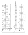
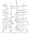
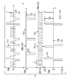
- FIGS. 6A , 7 , 9A , 9B , 10A , and 11A The feedback modulation of the phase of the counter-propagating lightwaves as imparted at the phase modulator 14 is depicted waveforms in FIGS. 6A , 7 , 9A , 9B , 10A , and 11A .
- This is an intermediate step to creating the resultant waveforms of the modulation of the difference between the phases of the two waves as they interfere with each other at the detector.
- FIGS. 6C , 9C , 10B , and 11B emphasis will be placed on describing this phase-difference modulation as well as the resultant detected optical power in FIGS. 12-14 .
- the prior art dual-staircase waveforms are shown in FIGS. 6A , 6B , and 6C and discussed in detail in U.S. patent 7505139 .
- the phase modulation is shown in FIG. 6A-6C for a particular rotation rate and therefore a particular rotation-rate induced phase shift. This rotation rate, and corresponding phase shift of about minus ⁇ /6, is selected for illustrative purposes, but it is not an atypical rate rotation rate.
- the bias phase-difference modulation waveform is shown in FIG. 6B signal 804.
- the phase difference that compensates for the rotation-rate phase difference is shown in FIG. 6B signal 802.
- the calibration phase difference waveform together with the readjustment phase-difference modulation is shown in FIG. 6B signal 803.
- the total phase difference modulation is shown in signal 801.
- the total phase modulation waveform applied to the waves at the phase modulator (701) becomes the modulation of the total phase-difference between the waves (801) as they interfere at the detector.
- digital values at the input of the feedback accumulator 30 correspond to the phase difference modulation, signal 801
- digital values at the output of the feedback accumulator 30 correspond to the phase modulation, signal 701.
- the phase-difference modulation waveform 801 is unchanged in FIGS. 6C and 9C .
- the component phase modulation waveforms are different however: waveform 805 in FIG. 9C is shifted in time compared to waveform 804 in FIG. 6C and the calibration phase modulation 807 uses the values of 0, plus 2 ⁇ , and minus 2 ⁇ instead of the values of plus ⁇ and minus ⁇ used in component waveform 803 FIG. 6C .
- This new way of displaying the component waveforms makes it easier to make the transition to the occasional calibration waveform shown in FIG. 10A , 10B , 11A , and 11B .
- the phase difference modulation waveforms 801, 808, and 810 are designed to accomplish four major tasks simultaneously, and can be understood as the sum of four separate waveforms.
- the first of these four waveforms is a bias modulation waveform 805 (See FIGS. 9B , 9C , 10B and 11C ) that enables the electronics to create a demodulated error signal that is linearly related to any additional phase differences over a limited range.
- the second is the RRFPDM 802 (See FIGS. 9B , 9C , 10B , and 11B ) that compensates for the phase difference due to rotation.
- the third waveform is the CFPDM 807 in FIG. 9C and 809 in FIG. 10B and 811 in FIG. 11B .
- These calibration phase difference modulations CFPDM all enable the measurement of the transfer function between the digital electronics and the phase difference modulation created via the phase modulator 14. They are distinctly different from the waveform 806 that adjusts the phase difference to keep it within a predetermined range. This is distinctly different from the prior art component waveform 803 in FIGS.
- the close-loop signal processing and digital-to-analog conversion electronics 13 is configured so that the variation in the demodulated error signal as a function of the difference in phase produced between the two waves in the neighborhood of i ⁇ is approximately linear, where i is an integer.
- This arrangement makes it possible to obtain a very high sensitivity of the variation in the demodulated error signal in the neighborhood of the i ⁇ in the phase difference. It is readily appreciated that without the bias modulation the dependency of the detected optical power on the phase difference is of cosine form, and the sensitivity in the i ⁇ neighborhood of the phase difference is very low.
- the preferred bias phase modulation signal is a square wave with period equal to 2 ⁇ and peak-to-peak amplitude ⁇ mbm . This creates a phase difference modulation with the same period 2 ⁇ , but with twice the amplitude alternating back and forth from + ⁇ mbm to - ⁇ mbm .
- the demodulated signal is of sine form that is linear in the neighborhood of i ⁇ , where i is any integer or zero.
- phase difference 802 that is equal and opposite the phase difference created by the rotation rate. That is to say that when the rotation rate introduces a phase difference between the two waves in the interferometer, this difference produces a variation in the signal emitted by the detector 11 provoking, via the signal processor 13 and the phase modulator 14, an action that is equally and oppositely directed to the phase shift produced initially, so that the sum of these two phase differences is brought back to the null value.
- signal processor 13 generates a staircase negative feedback signal 702. Each step has duration of ⁇ and a step height that is on average equal to the phase difference due to rotation rate.
- phase modulation waveform that is used to measure the transfer function between digital values and actual phase modulation.
- Signal processor 13 is configured to add this fourth waveform component (807 in FIG. 9C , 809 in FIG. 10B , and 811 in FIG. 11B ) that shifts the operating phase difference alternately between values of zero and 2 ⁇ in one direction for duration ⁇ and then 2 ⁇ in the other direction on a subsequent ⁇ and back to zero.
- the swing to minus 2 ⁇ occurs right after the swing to plus 2 ⁇ .
- the total phase difference, including the bias modulation, is then 2 ⁇ - ⁇ mbm or ⁇ mbm - 2 ⁇ .
- the four components of the phase modulation are synchronous with each other.
- the constant portions occur at the same time, and likewise the transitions from one constant value to another also coincide in time.
- FIG. 10A shows phase modulation 708 and phase modulation components 702, 705, 706 and 709. These correspond directly to FIG. 10B phase-difference modulation 808 and phase-difference modulation components 802, 805, 806 and 809.
- waveform 802 Yet summing waveforms 802, 803, and 804 yields the same waveform 801 as summing 802 plus 805 plus 806 plus 807.
- accumulating waveform 801 once per ⁇ gives waveform 701.
- accumulating waveform 808 once per ⁇ gives waveform 708.
- Waveform 708 is a sequence of 2 or more steps up, followed by a sequence of 2 or more steps down, in addition to sequences of back and forth of up-steps and down-steps.
- FIGS. 6A nd 9 accumulating waveform 801 once per ⁇ gives waveform 701.
- FIGS. 10A and 10B accumulating waveform 808 once per ⁇ gives waveform 708.
- Waveform 708 is a sequence of 2 or more steps up, followed by a sequence of 2 or more steps down, in addition to sequences of back and forth of up-steps and down-steps.
- the phase-modulation waveform 708 shown in FIG. 10A is designed to accomplish three main tasks: first it makes the interferometer sensitive to small changes in Sagnac phase difference due to rotating the gyroscope (this is commonly referred to as biasing the interferometer); second, it supplies a feedback phase difference to keep the interferometer sensitive to small changes in rotation rate; and third, it supplies the calibration modulation necessary to keep the digital electronics calibrated with respect to the Sagnac phase difference being measured.
- the calibration task is accomplished by the occasional dual-staircase waveform where two steps are taken in one direction and then two steps are taken in the other. In prior art, the dual-staircase sections of the waveform occur one after another. The prior art approach has led to an unacceptable amount of measurement error in some gyroscopes. Dispersing the dual-staircase sections as shown reduces this error.
- FIG. 12A-FIG. 12D there shown is a phase modulation waveform of the present invention ( FIG. 12A ) applied at the phase modulator together with the Sagnac phase difference becomes the total phase difference ( FIG. 12B ) as the two waves from the interferometer are brought together.
- the interferogram FIG. 12C ) shows how the phase difference is transformed into optical power vs. time ( FIG. 12D ).
- the phase difference modulation adds to the Sagnac phase difference to create the total phase difference between the counter-propagating waves at the detector, shown in FIG. 12B .
- the graph of optical power vs. phase difference between the interfering waves is shown in FIG. 12C and is known as the interferogram.
- the interferogram, FIG. 12C maps the total phase difference to detected optical power, and therefore it maps the total phase difference vs. time, FIG. 12B , into the detected optical power vs. time, FIG. 12D .
- FIG. 13A- FIG. 13C show how an error in the rotation-rate digital value will affect the total phase difference ( FIG. 13A ) and the detected optical power, ( FIG. 13C ).
- the rotation-rate demodulator will multiply the detector optical power by the square wave reference signal and will create the rotation-rate error signal that will be used by the rotation-rate accumulator to correct the rotation-rate digital value. Once the rotation-rate digital value is correct the power signal will be flat and the rotation-rate error signal will be zero.
- FIG. 14A- FIG. 14C show how an error in the 2 ⁇ DS will affect the total phase difference ( FIG. 14A ) and the detected optical power ( FIG. 14C ).
- the calibration demodulator will multiply the detector optical power by the calibration reference signal and will create the calibration error signal that will be used by the calibration accumulator to correct the 2 ⁇ DS.
- FIGS. 11A and 11B there shown is a modified sequence for a calibration waveform.
- the sequence may be modified to sometimes use 0, +2 ⁇ , -2 ⁇ , and 0 and other times use 0, -2 ⁇ , +2 ⁇ , and 0 in waveform 808 as shown in FIG. 11B . This can reduce total phase modulation required and thus reduce the voltage necessary to effect the modulation.
- a dual-staircase calibration phase-difference modulation is created within the calibration control loop.
- This new dual-staircase calibration phase-difference modulation can be described in terms of two sequences. Each sequence contains a series of phase-difference steps and each step has duration of ⁇ .
- a first sequence consists of one or more of a first group of phase-difference steps. The first group is a zero step followed by a 2 ⁇ step.
- a second sequence is one or more of a second group of steps. The second group consists of a minus 2 ⁇ step followed by a zero step.
- the calibration phase-difference modulation then consists of one after the other of first sequences followed by second sequences as shown in waveform 809 ( FIG. 10B ).
- Adding bias phase-difference modulation of waveform 805 and rotation-rate nulling phase difference waveform 802 to the dual-staircase calibration phase-difference modulation of waveform 809 and adjustment waveform 806 gives a dual-staircase total phase difference modulation of waveform 808. Passing this dual-staircase total phase difference modulation through the feedback accumulator 30 makes a dual staircase phase modulation of 708 ( FIG. 10A ).
- the calibration loop in the dual staircase approach determines a digital value that corresponds to a fixed phase shift.
- the calibration loop of the dual staircase approach measures the relationship between the digital values of the signal processing and a phase modulation of 2 ⁇ radians, but it does not impose a relationship as in a calibration loop of a prior art staircase-and-fall-back approach.
- the third sequence is added to the calibration phase difference modulation.
- the third sequence consists of pairs of null steps.
- the occasional-calibration-approach-calibration-phase-difference modulation consists of a first sequence, a second sequence and a third sequence.
- the calibration is accomplished by the first and second sequences.
- the third sequence can include a large number of pairs.
- the third sequence does not contribute any error to the rotation rate measurement that the first and second sequences might contribute.
- the occasional calibration waveform dual-staircase signal processing of the present invention is significantly better than the prior-art staircase-and-fall-back or dual staircase approaches.
- the prior art approaches have led to an unacceptable amount of measurement error in some gyroscopes.
- the occasional-calibration-dual-staircase approach is much better than the staircase-and-fallback approach because the feedback gain of the calibration loop is not proportional to the rotation rate.
- the occasional-calibration-dual-staircase approach is much better than the standard dual-staircase approach because by dispersing the dual-staircase sequences as shown, for example, in waveform 808 ( FIG. 10A ) and error present in some fiber optic gyroscopes (FOGs) is significantly reduced.
Landscapes
- Engineering & Computer Science (AREA)
- Physics & Mathematics (AREA)
- Power Engineering (AREA)
- Optics & Photonics (AREA)
- Electromagnetism (AREA)
- General Physics & Mathematics (AREA)
- Radar, Positioning & Navigation (AREA)
- Remote Sensing (AREA)
- Gyroscopes (AREA)
Claims (15)
- Procédé de modulation de la différence de phase entre une paire d'ondes optiques sortant d'une partie d'interféromètre de Sagnac d'un gyroscope à fibre optique, dans lequel un signal de modulation de phase (701) est appliqué à un modulateur de phase (14) afin de moduler la phase de ladite paire d'ondes pendant que ladite paire d'ondes se propage dans des directions opposées à travers le modulateur de phase (14) et en raison du fait que le modulateur de phase n'est pas au centre de la partie d'interféromètre de Sagnac d'un gyroscope à fibre optique, ladite modulation de phase provoque une modulation de la différence de phase entre les deux ondes lorsqu'elles sortent de la partie d'interféromètre de Sagnac d'un gyroscope à fibre optique et arrivent au niveau du détecteur (11), la modulation de différence de phase (801) étant une somme des composantes de différence de phase suivantes :(i) une composante de modulation de différence de phase de polarisation (805) ayant une amplitude de modulation de polarisation et une forme d'onde sélectionnées,(ii) une composante de modulation de différence de phase à rétroaction de vitesse de rotation (802),(iii) une composante de différence de phase d'ajustement de forme d'onde (806) qui prend des valeurs non nulles pendant les périodes temporelles d'ajustement afin de maintenir la modulation de phase dans une plage prédéterminée,
caractérisé en ce que la modulation de différence de phase comprend en outre :(iv) une composante de modulation de différence de phase à rétroaction d'étalonnage (807 ; 809 ; 811)et en ce que le procédé comprend l'activation de ladite composante de modulation de différence de phase à rétroaction d'étalonnage (807 ; 809 ; 811) pendant des premières périodes temporelles, et la désactivation de ladite composante de modulation de différence de phase à rétroaction d'étalonnage (807 ; 809 ; 811) pendant de secondes périodes temporelles pendant lesquelles ladite composante de modulation de différence de phase à rétroaction d'étalonnage est sensiblement nulle. - Procédé selon la revendication 1, dans lequel lesdites premières périodes temporelles ont lieu à des moments qui sont différents desdites périodes temporelles d'ajustement.
- Procédé selon la revendication 1, dans lequel la durée d'activation et la durée de désactivation sont sensiblement indépendantes de la vitesse de rotation.
- Procédé selon la revendication 1, dans lequel l'activation de ladite modulation de phase à rétroaction d'étalonnage coïncide avec les étapes du signal de composante d'ajustement de forme d'onde moins de 50 pour cent du temps.
- Procédé selon la revendication 1, dans lequel l'activation de ladite modulation de différence de phase à rétroaction d'étalonnage coïncide avec les étapes du signal de composante d'ajustement de forme d'onde moins de 25 pour cent du temps.
- Procédé selon la revendication 2, dans lequel le signal de composante de modulation d'étalonnage (809 ; 811) est activé moins de 10 pour cent de la période temporelle.
- Procédé selon la revendication 1, dans lequel la modulation de la phase d'ondes lumineuses dans la partie d'interféromètre de Sagnac d'un gyroscope à fibre optique est réalisée selon une forme d'onde de modulation de phase par rapport au temps (708) comprenant des valeurs constantes pour une durée temporelle et des transitions entre des valeurs constantes, et dans lequel une combinaison d'une transition et d'une valeur constante immédiatement après est appelée étape de modulation de phase ; et une étape de hausse de modulation de phase est une transition et une valeur constante dans lequel ladite transition se fait d'une valeur constante plus petite à une valeur constante plus grande, et une étape de diminution de modulation de phase comprend une transition et une valeur constante dans lequel ladite transition se fait d'une valeur plus grande à une valeur plus petite, et ladite forme d'onde de modulation de phase inclut trois séquences d'étapes de phase :i. une première séquence comprend une pluralité d'étapes de hausse les unes après les autres,ii. une deuxième séquence comprend une pluralité d'étapes de diminution les unes après les autres, etiii. une troisième séquence comprend à la fois des étapes de hausse et des étapes de diminution et alterne entre des étapes de hausse unique et des étapes de diminution unique, un exemple d'une troisième séquence est une série répétée d'une étape de hausse, suivie d'une étape de diminution.
- Procédé selon la revendication 7, dans lequel lesdites trois séquences sont toutes présentes pour mesurer une différence de phase de Sagnac non nulle donnée.
- Procédé selon la revendication 7, dans lequel une durée d'étape incluant une durée de transition plus la durée de la valeur constante est sensiblement égale à un τ, où τ est une différence temporelle de propagation d'onde optique entre des trajets courts et longs du modulateur de phase (14) au détecteur (11).
- Procédé selon la revendication 8, dans lequel une durée d'étape incluant une durée de transition et la durée de la valeur constante est sensiblement égale à un τ, où τ est une différence temporelle de propagation d'onde optique entre des trajets courts et longs du modulateur de phase (14) au détecteur (11).
- Procédé selon la revendication 1, dans lequel ledit signal de modulation de phase inclut des séquences d'étapes en phase, une séquence après l'autre, incluant :(i) une première séquence qui alterne entre des étapes de hausse de modulation de phase et des étapes de diminution de modulation de phase, une étape de hausse étant suivie d'une étape de diminution, où la séquence se répète de multiples fois,(ii) une deuxième séquence qui comprend deux étapes ou plus dans une direction, immédiatement suivies de deux étapes ou plus dans l'autre direction, deux étapes de hausse suivies de deux étapes de diminution, dans lequel une étape de hausse de modulation de phase est une transition et une valeur constante dans lequel ladite transition se fait d'une valeur constante plus petite à une valeur constante plus grande, et une étape de diminution de modulation de phase comprend une transition et une valeur constante dans lequel ladite transition se fait d'une valeur plus grande à une valeur plus petite.
- Procédé selon la revendication 11, dans lequel ledit signal de modulation de phase alterne entre lesdites premières séquences et lesdites deuxièmes séquences.
- Procédé selon la revendication 11, dans lequel la durée de chaque étape est approximativement égale à τ, où τ est une différence temporelle de propagation d'onde optique entre des trajets courts et longs du modulateur de phase (14) au détecteur (11).
- Procédé selon la revendication 13, dans lequel davantage de temps s'écoule pendant les premières séquences que pendant les deuxièmes séquences.
- Procédé selon la revendication 13, dans lequel le nombre total d'étapes dans les premières séquences est au moins dix fois le nombre total d'étapes dans les deuxièmes séquences.
Applications Claiming Priority (1)
| Application Number | Priority Date | Filing Date | Title |
|---|---|---|---|
| PCT/US2010/041949 WO2012008955A1 (fr) | 2010-07-14 | 2010-07-14 | Modulation de différence de phase d'étalonnage par intermittence pour interféromètre de sagnac |
Publications (3)
| Publication Number | Publication Date |
|---|---|
| EP2593749A1 EP2593749A1 (fr) | 2013-05-22 |
| EP2593749A4 EP2593749A4 (fr) | 2014-01-22 |
| EP2593749B1 true EP2593749B1 (fr) | 2015-10-07 |
Family
ID=45469727
Family Applications (1)
| Application Number | Title | Priority Date | Filing Date |
|---|---|---|---|
| EP10854823.1A Not-in-force EP2593749B1 (fr) | 2010-07-14 | 2010-07-14 | Modulation de différence de phase d'étalonnage par intermittence pour interféromètre de sagnac |
Country Status (3)
| Country | Link |
|---|---|
| US (1) | US8610995B2 (fr) |
| EP (1) | EP2593749B1 (fr) |
| WO (1) | WO2012008955A1 (fr) |
Families Citing this family (9)
| Publication number | Priority date | Publication date | Assignee | Title |
|---|---|---|---|---|
| US8497994B2 (en) | 2008-02-14 | 2013-07-30 | Ralph A. Bergh | Interferometer employing a multi-waveguide optical loop path and fiber optic rotation rate sensor employing same |
| US9518827B2 (en) | 2010-05-07 | 2016-12-13 | Ralph A. Bergh | Method and apparatus for multiplexing multiple Sagnac interferometers with single input for source light |
| FR2987111B1 (fr) * | 2012-02-21 | 2014-03-07 | Ixblue | Dispositif de mesure a fibre optique, gyrometre, centrale de navigation et de stabilisation inertielle |
| FR2990021B1 (fr) * | 2012-04-27 | 2014-05-09 | Ixblue | Dispositif de mesure a fibre optique, gyrometre, centrale de navigation et de stabilisation inertielle. |
| CN103940593B (zh) * | 2014-04-28 | 2016-05-25 | 浙江大学 | 一种基于数字锯齿波的光纤陀螺渡越时间快速测量方法 |
| US9495801B2 (en) | 2014-05-01 | 2016-11-15 | Microsoft Technology Licensing, Llc | Pose tracking an augmented reality device |
| ITUB20161106A1 (it) * | 2016-02-26 | 2016-05-26 | Civitanavi Systems S R L | Giroscopio in fibra ottica interferometrico I-FOG. |
| WO2019220410A1 (fr) * | 2018-05-17 | 2019-11-21 | Institut National De La Recherche Scientifique (Inrs) | Procédé et système d'échantillonnage et de débruitage d'une amplification de signal |
| CN111174773B (zh) * | 2019-12-30 | 2022-04-05 | 浙江大学 | 一种多相调制解调的光纤陀螺多闭环算法 |
Family Cites Families (13)
| Publication number | Priority date | Publication date | Assignee | Title |
|---|---|---|---|---|
| US4299490A (en) | 1978-12-07 | 1981-11-10 | Mcdonnell Douglas Corporation | Phase nulling optical gyro |
| US4634282A (en) | 1981-11-06 | 1987-01-06 | The Board Of Trustees Of The Leland Stanford Junior University | Multimode fiber optic rotation sensor |
| DE3426868A1 (de) | 1984-07-20 | 1986-01-30 | LITEF Litton Technische Werke der Hellige GmbH, 7800 Freiburg | Verfahren und einrichtung zur drehratenauslesung mittels eines passiven optischen resonators |
| US4869592A (en) * | 1988-01-27 | 1989-09-26 | Bergh Ralph A | Method and apparatus for obtaining a digital measure of absolute rotation |
| FR2654827B1 (fr) | 1989-11-17 | 1992-03-20 | Photonetics | Dispositif de mesure a fibre optique, gyrometre, centrale de navigation et de stabilisation. |
| FR2660996B1 (fr) * | 1990-04-17 | 1992-08-07 | Photonetics | Dispositif de mesure a fibre optique, gyrometre, centrale de navigation et de stabilisation, capteur de courant. |
| DE59307220D1 (de) * | 1993-10-28 | 1997-10-02 | Litef Gmbh | Faseroptisches Sagnac-Interferometer zur Drehratenmessung mit wellenlängenstabilisierter Lichtquelle |
| US6539151B2 (en) | 2000-08-21 | 2003-03-25 | Corning, Incorporated | Method for making separable multiple core optical fibers, the resulting fiber structures, and uses thereof |
| US6826343B2 (en) | 2001-03-16 | 2004-11-30 | Cidra Corporation | Multi-core waveguide |
| US6744519B2 (en) * | 2002-04-30 | 2004-06-01 | Honeywell International Inc. | Methods and apparatus for fiber optic gyroscope dead band error suppression modulation |
| US7167250B2 (en) * | 2002-04-30 | 2007-01-23 | Honeywell International, Inc. | System and method for reducing fiber optic gyroscope color noise |
| US7664347B2 (en) | 2006-06-07 | 2010-02-16 | Baker Hughes Incorporated | Multi-core optical fiber sensor |
| US7505139B2 (en) | 2007-03-06 | 2009-03-17 | Bergh Ralph A | Signal processing for a Sagnac interferometer |
-
2010
- 2010-07-14 EP EP10854823.1A patent/EP2593749B1/fr not_active Not-in-force
- 2010-07-14 WO PCT/US2010/041949 patent/WO2012008955A1/fr not_active Ceased
- 2010-07-14 US US13/388,924 patent/US8610995B2/en active Active
Also Published As
| Publication number | Publication date |
|---|---|
| EP2593749A1 (fr) | 2013-05-22 |
| EP2593749A4 (fr) | 2014-01-22 |
| US8610995B2 (en) | 2013-12-17 |
| US20120134005A1 (en) | 2012-05-31 |
| WO2012008955A1 (fr) | 2012-01-19 |
Similar Documents
| Publication | Publication Date | Title |
|---|---|---|
| EP2593749B1 (fr) | Modulation de différence de phase d'étalonnage par intermittence pour interféromètre de sagnac | |
| JP2878441B2 (ja) | ファイバー光測定装置、ジャイロメータ、セントラルナビゲーション、及び安定化システム | |
| US7505139B2 (en) | Signal processing for a Sagnac interferometer | |
| US5181078A (en) | Fiber optic measuring device, rate gyro, navigation and stabilization system, and current sensor | |
| JP4130730B2 (ja) | 光ファイバジャイロスコープ | |
| US7038783B2 (en) | Eigen frequency detector for Sagnac interferometers | |
| JP3990450B2 (ja) | 光ファイバ感知コイル用の固有周波数トラッカ | |
| JPH047931B2 (fr) | ||
| JP5362180B2 (ja) | 光ファイバ・ジャイロスコープの非同期復調 | |
| WO1998058235A1 (fr) | Compensateur d'erreurs de vibrations pour un gyroscope a fibres optiques | |
| US5530545A (en) | Method for reducing random walk in fiber optic gyroscopes | |
| US4872754A (en) | Constant frequency digital closed-loop optical fiber gyro | |
| RU2620933C1 (ru) | Волоконно-оптический гироскоп с большим динамическим диапазоном измерения угловых скоростей | |
| JP3266318B2 (ja) | 光ファイバ測定装置、ジャイロメータ、航法及び安定化用中央ユニット | |
| US5278631A (en) | Closed loop fiber optic gyroscope with signal processing arrangement for improved performance | |
| JP3343767B2 (ja) | 光ファイバジャイロ | |
| US5650849A (en) | Optical rate sensor having modulated clockwise and counterclockwise beams | |
| JPS63250513A (ja) | 光フアイバジヤイロ | |
| RU2627020C1 (ru) | Способ повышения точности волоконно-оптических гироскопов при воздействии вибраций | |
| JP3245796B2 (ja) | 光ファイバジャイロ | |
| JP2000155031A (ja) | 光ファイバジャイロ | |
| JP3923077B2 (ja) | 光ファイバ・ジャイロスコープのランダム・ウオークを減少する方法 | |
| JPH0942974A (ja) | 光ファイバジャイロ | |
| JPH0545114A (ja) | 干渉計における位相推移の測定装置 | |
| GB2282879A (en) | Optical gyroscopes |
Legal Events
| Date | Code | Title | Description |
|---|---|---|---|
| PUAI | Public reference made under article 153(3) epc to a published international application that has entered the european phase |
Free format text: ORIGINAL CODE: 0009012 |
|
| 17P | Request for examination filed |
Effective date: 20130214 |
|
| AK | Designated contracting states |
Kind code of ref document: A1 Designated state(s): AL AT BE BG CH CY CZ DE DK EE ES FI FR GB GR HR HU IE IS IT LI LT LU LV MC MK MT NL NO PL PT RO SE SI SK SM TR |
|
| DAX | Request for extension of the european patent (deleted) | ||
| A4 | Supplementary search report drawn up and despatched |
Effective date: 20140107 |
|
| RIC1 | Information provided on ipc code assigned before grant |
Ipc: G01C 19/72 20060101AFI20131219BHEP Ipc: G01C 19/64 20060101ALI20131219BHEP Ipc: G02B 6/26 20060101ALI20131219BHEP |
|
| GRAP | Despatch of communication of intention to grant a patent |
Free format text: ORIGINAL CODE: EPIDOSNIGR1 |
|
| INTG | Intention to grant announced |
Effective date: 20150320 |
|
| GRAS | Grant fee paid |
Free format text: ORIGINAL CODE: EPIDOSNIGR3 |
|
| GRAR | Information related to intention to grant a patent recorded |
Free format text: ORIGINAL CODE: EPIDOSNIGR71 |
|
| GRAA | (expected) grant |
Free format text: ORIGINAL CODE: 0009210 |
|
| INTG | Intention to grant announced |
Effective date: 20150827 |
|
| AK | Designated contracting states |
Kind code of ref document: B1 Designated state(s): AL AT BE BG CH CY CZ DE DK EE ES FI FR GB GR HR HU IE IS IT LI LT LU LV MC MK MT NL NO PL PT RO SE SI SK SM TR |
|
| REG | Reference to a national code |
Ref country code: GB Ref legal event code: FG4D |
|
| REG | Reference to a national code |
Ref country code: AT Ref legal event code: REF Ref document number: 754014 Country of ref document: AT Kind code of ref document: T Effective date: 20151015 Ref country code: CH Ref legal event code: EP |
|
| REG | Reference to a national code |
Ref country code: IE Ref legal event code: FG4D |
|
| REG | Reference to a national code |
Ref country code: DE Ref legal event code: R096 Ref document number: 602010028146 Country of ref document: DE |
|
| REG | Reference to a national code |
Ref country code: NL Ref legal event code: MP Effective date: 20151007 |
|
| REG | Reference to a national code |
Ref country code: AT Ref legal event code: MK05 Ref document number: 754014 Country of ref document: AT Kind code of ref document: T Effective date: 20151007 |
|
| REG | Reference to a national code |
Ref country code: LT Ref legal event code: MG4D |
|
| PG25 | Lapsed in a contracting state [announced via postgrant information from national office to epo] |
Ref country code: LT Free format text: LAPSE BECAUSE OF FAILURE TO SUBMIT A TRANSLATION OF THE DESCRIPTION OR TO PAY THE FEE WITHIN THE PRESCRIBED TIME-LIMIT Effective date: 20151007 Ref country code: IS Free format text: LAPSE BECAUSE OF FAILURE TO SUBMIT A TRANSLATION OF THE DESCRIPTION OR TO PAY THE FEE WITHIN THE PRESCRIBED TIME-LIMIT Effective date: 20160207 Ref country code: NO Free format text: LAPSE BECAUSE OF FAILURE TO SUBMIT A TRANSLATION OF THE DESCRIPTION OR TO PAY THE FEE WITHIN THE PRESCRIBED TIME-LIMIT Effective date: 20160107 Ref country code: IT Free format text: LAPSE BECAUSE OF FAILURE TO SUBMIT A TRANSLATION OF THE DESCRIPTION OR TO PAY THE FEE WITHIN THE PRESCRIBED TIME-LIMIT Effective date: 20151007 Ref country code: ES Free format text: LAPSE BECAUSE OF FAILURE TO SUBMIT A TRANSLATION OF THE DESCRIPTION OR TO PAY THE FEE WITHIN THE PRESCRIBED TIME-LIMIT Effective date: 20151007 Ref country code: HR Free format text: LAPSE BECAUSE OF FAILURE TO SUBMIT A TRANSLATION OF THE DESCRIPTION OR TO PAY THE FEE WITHIN THE PRESCRIBED TIME-LIMIT Effective date: 20151007 Ref country code: NL Free format text: LAPSE BECAUSE OF FAILURE TO SUBMIT A TRANSLATION OF THE DESCRIPTION OR TO PAY THE FEE WITHIN THE PRESCRIBED TIME-LIMIT Effective date: 20151007 |
|
| PG25 | Lapsed in a contracting state [announced via postgrant information from national office to epo] |
Ref country code: PT Free format text: LAPSE BECAUSE OF FAILURE TO SUBMIT A TRANSLATION OF THE DESCRIPTION OR TO PAY THE FEE WITHIN THE PRESCRIBED TIME-LIMIT Effective date: 20160208 Ref country code: AT Free format text: LAPSE BECAUSE OF FAILURE TO SUBMIT A TRANSLATION OF THE DESCRIPTION OR TO PAY THE FEE WITHIN THE PRESCRIBED TIME-LIMIT Effective date: 20151007 Ref country code: GR Free format text: LAPSE BECAUSE OF FAILURE TO SUBMIT A TRANSLATION OF THE DESCRIPTION OR TO PAY THE FEE WITHIN THE PRESCRIBED TIME-LIMIT Effective date: 20160108 Ref country code: LV Free format text: LAPSE BECAUSE OF FAILURE TO SUBMIT A TRANSLATION OF THE DESCRIPTION OR TO PAY THE FEE WITHIN THE PRESCRIBED TIME-LIMIT Effective date: 20151007 Ref country code: PL Free format text: LAPSE BECAUSE OF FAILURE TO SUBMIT A TRANSLATION OF THE DESCRIPTION OR TO PAY THE FEE WITHIN THE PRESCRIBED TIME-LIMIT Effective date: 20151007 Ref country code: SE Free format text: LAPSE BECAUSE OF FAILURE TO SUBMIT A TRANSLATION OF THE DESCRIPTION OR TO PAY THE FEE WITHIN THE PRESCRIBED TIME-LIMIT Effective date: 20151007 Ref country code: FI Free format text: LAPSE BECAUSE OF FAILURE TO SUBMIT A TRANSLATION OF THE DESCRIPTION OR TO PAY THE FEE WITHIN THE PRESCRIBED TIME-LIMIT Effective date: 20151007 |
|
| REG | Reference to a national code |
Ref country code: FR Ref legal event code: PLFP Year of fee payment: 7 |
|
| REG | Reference to a national code |
Ref country code: DE Ref legal event code: R097 Ref document number: 602010028146 Country of ref document: DE |
|
| PG25 | Lapsed in a contracting state [announced via postgrant information from national office to epo] |
Ref country code: CZ Free format text: LAPSE BECAUSE OF FAILURE TO SUBMIT A TRANSLATION OF THE DESCRIPTION OR TO PAY THE FEE WITHIN THE PRESCRIBED TIME-LIMIT Effective date: 20151007 |
|
| PLBE | No opposition filed within time limit |
Free format text: ORIGINAL CODE: 0009261 |
|
| STAA | Information on the status of an ep patent application or granted ep patent |
Free format text: STATUS: NO OPPOSITION FILED WITHIN TIME LIMIT |
|
| PG25 | Lapsed in a contracting state [announced via postgrant information from national office to epo] |
Ref country code: SK Free format text: LAPSE BECAUSE OF FAILURE TO SUBMIT A TRANSLATION OF THE DESCRIPTION OR TO PAY THE FEE WITHIN THE PRESCRIBED TIME-LIMIT Effective date: 20151007 Ref country code: SM Free format text: LAPSE BECAUSE OF FAILURE TO SUBMIT A TRANSLATION OF THE DESCRIPTION OR TO PAY THE FEE WITHIN THE PRESCRIBED TIME-LIMIT Effective date: 20151007 Ref country code: RO Free format text: LAPSE BECAUSE OF FAILURE TO SUBMIT A TRANSLATION OF THE DESCRIPTION OR TO PAY THE FEE WITHIN THE PRESCRIBED TIME-LIMIT Effective date: 20151007 Ref country code: DK Free format text: LAPSE BECAUSE OF FAILURE TO SUBMIT A TRANSLATION OF THE DESCRIPTION OR TO PAY THE FEE WITHIN THE PRESCRIBED TIME-LIMIT Effective date: 20151007 Ref country code: EE Free format text: LAPSE BECAUSE OF FAILURE TO SUBMIT A TRANSLATION OF THE DESCRIPTION OR TO PAY THE FEE WITHIN THE PRESCRIBED TIME-LIMIT Effective date: 20151007 |
|
| 26N | No opposition filed |
Effective date: 20160708 |
|
| PGFP | Annual fee paid to national office [announced via postgrant information from national office to epo] |
Ref country code: DE Payment date: 20160705 Year of fee payment: 7 |
|
| PG25 | Lapsed in a contracting state [announced via postgrant information from national office to epo] |
Ref country code: SI Free format text: LAPSE BECAUSE OF FAILURE TO SUBMIT A TRANSLATION OF THE DESCRIPTION OR TO PAY THE FEE WITHIN THE PRESCRIBED TIME-LIMIT Effective date: 20151007 |
|
| PG25 | Lapsed in a contracting state [announced via postgrant information from national office to epo] |
Ref country code: BE Free format text: LAPSE BECAUSE OF FAILURE TO SUBMIT A TRANSLATION OF THE DESCRIPTION OR TO PAY THE FEE WITHIN THE PRESCRIBED TIME-LIMIT Effective date: 20151007 |
|
| REG | Reference to a national code |
Ref country code: CH Ref legal event code: PL |
|
| PG25 | Lapsed in a contracting state [announced via postgrant information from national office to epo] |
Ref country code: MC Free format text: LAPSE BECAUSE OF FAILURE TO SUBMIT A TRANSLATION OF THE DESCRIPTION OR TO PAY THE FEE WITHIN THE PRESCRIBED TIME-LIMIT Effective date: 20151007 |
|
| PG25 | Lapsed in a contracting state [announced via postgrant information from national office to epo] |
Ref country code: LI Free format text: LAPSE BECAUSE OF NON-PAYMENT OF DUE FEES Effective date: 20160731 Ref country code: CH Free format text: LAPSE BECAUSE OF NON-PAYMENT OF DUE FEES Effective date: 20160731 |
|
| REG | Reference to a national code |
Ref country code: IE Ref legal event code: MM4A |
|
| REG | Reference to a national code |
Ref country code: FR Ref legal event code: PLFP Year of fee payment: 8 |
|
| PG25 | Lapsed in a contracting state [announced via postgrant information from national office to epo] |
Ref country code: IE Free format text: LAPSE BECAUSE OF NON-PAYMENT OF DUE FEES Effective date: 20160714 |
|
| PG25 | Lapsed in a contracting state [announced via postgrant information from national office to epo] |
Ref country code: LU Free format text: LAPSE BECAUSE OF NON-PAYMENT OF DUE FEES Effective date: 20160714 |
|
| PGFP | Annual fee paid to national office [announced via postgrant information from national office to epo] |
Ref country code: GB Payment date: 20170719 Year of fee payment: 8 Ref country code: FR Payment date: 20170728 Year of fee payment: 8 |
|
| REG | Reference to a national code |
Ref country code: DE Ref legal event code: R119 Ref document number: 602010028146 Country of ref document: DE |
|
| PG25 | Lapsed in a contracting state [announced via postgrant information from national office to epo] |
Ref country code: DE Free format text: LAPSE BECAUSE OF NON-PAYMENT OF DUE FEES Effective date: 20180201 |
|
| PG25 | Lapsed in a contracting state [announced via postgrant information from national office to epo] |
Ref country code: HU Free format text: LAPSE BECAUSE OF FAILURE TO SUBMIT A TRANSLATION OF THE DESCRIPTION OR TO PAY THE FEE WITHIN THE PRESCRIBED TIME-LIMIT; INVALID AB INITIO Effective date: 20100714 Ref country code: CY Free format text: LAPSE BECAUSE OF FAILURE TO SUBMIT A TRANSLATION OF THE DESCRIPTION OR TO PAY THE FEE WITHIN THE PRESCRIBED TIME-LIMIT Effective date: 20151007 |
|
| PG25 | Lapsed in a contracting state [announced via postgrant information from national office to epo] |
Ref country code: MK Free format text: LAPSE BECAUSE OF FAILURE TO SUBMIT A TRANSLATION OF THE DESCRIPTION OR TO PAY THE FEE WITHIN THE PRESCRIBED TIME-LIMIT Effective date: 20151007 Ref country code: MT Free format text: LAPSE BECAUSE OF NON-PAYMENT OF DUE FEES Effective date: 20160731 Ref country code: TR Free format text: LAPSE BECAUSE OF FAILURE TO SUBMIT A TRANSLATION OF THE DESCRIPTION OR TO PAY THE FEE WITHIN THE PRESCRIBED TIME-LIMIT Effective date: 20151007 |
|
| PG25 | Lapsed in a contracting state [announced via postgrant information from national office to epo] |
Ref country code: BG Free format text: LAPSE BECAUSE OF FAILURE TO SUBMIT A TRANSLATION OF THE DESCRIPTION OR TO PAY THE FEE WITHIN THE PRESCRIBED TIME-LIMIT Effective date: 20151007 |
|
| PG25 | Lapsed in a contracting state [announced via postgrant information from national office to epo] |
Ref country code: AL Free format text: LAPSE BECAUSE OF FAILURE TO SUBMIT A TRANSLATION OF THE DESCRIPTION OR TO PAY THE FEE WITHIN THE PRESCRIBED TIME-LIMIT Effective date: 20151007 |
|
| GBPC | Gb: european patent ceased through non-payment of renewal fee |
Effective date: 20180714 |
|
| PG25 | Lapsed in a contracting state [announced via postgrant information from national office to epo] |
Ref country code: GB Free format text: LAPSE BECAUSE OF NON-PAYMENT OF DUE FEES Effective date: 20180714 Ref country code: FR Free format text: LAPSE BECAUSE OF NON-PAYMENT OF DUE FEES Effective date: 20180731 |