EP2597680A2 - Halbleiterbauelement - Google Patents
Halbleiterbauelement Download PDFInfo
- Publication number
- EP2597680A2 EP2597680A2 EP12193092.9A EP12193092A EP2597680A2 EP 2597680 A2 EP2597680 A2 EP 2597680A2 EP 12193092 A EP12193092 A EP 12193092A EP 2597680 A2 EP2597680 A2 EP 2597680A2
- Authority
- EP
- European Patent Office
- Prior art keywords
- region
- type
- buried
- main surface
- semiconductor substrate
- Prior art date
- Legal status (The legal status is an assumption and is not a legal conclusion. Google has not performed a legal analysis and makes no representation as to the accuracy of the status listed.)
- Withdrawn
Links
Images












Classifications
-
- H—ELECTRICITY
- H10—SEMICONDUCTOR DEVICES; ELECTRIC SOLID-STATE DEVICES NOT OTHERWISE PROVIDED FOR
- H10D—INORGANIC ELECTRIC SEMICONDUCTOR DEVICES
- H10D30/00—Field-effect transistors [FET]
- H10D30/60—Insulated-gate field-effect transistors [IGFET]
- H10D30/64—Double-diffused metal-oxide semiconductor [DMOS] FETs
- H10D30/65—Lateral DMOS [LDMOS] FETs
-
- H—ELECTRICITY
- H10—SEMICONDUCTOR DEVICES; ELECTRIC SOLID-STATE DEVICES NOT OTHERWISE PROVIDED FOR
- H10D—INORGANIC ELECTRIC SEMICONDUCTOR DEVICES
- H10D30/00—Field-effect transistors [FET]
- H10D30/01—Manufacture or treatment
- H10D30/021—Manufacture or treatment of FETs having insulated gates [IGFET]
- H10D30/0221—Manufacture or treatment of FETs having insulated gates [IGFET] having asymmetry in the channel direction, e.g. lateral high-voltage MISFETs having drain offset region or extended-drain MOSFETs [EDMOS]
-
- H—ELECTRICITY
- H10—SEMICONDUCTOR DEVICES; ELECTRIC SOLID-STATE DEVICES NOT OTHERWISE PROVIDED FOR
- H10D—INORGANIC ELECTRIC SEMICONDUCTOR DEVICES
- H10D30/00—Field-effect transistors [FET]
- H10D30/60—Insulated-gate field-effect transistors [IGFET]
- H10D30/601—Insulated-gate field-effect transistors [IGFET] having lightly-doped drain or source extensions, e.g. LDD IGFETs or DDD IGFETs
- H10D30/603—Insulated-gate field-effect transistors [IGFET] having lightly-doped drain or source extensions, e.g. LDD IGFETs or DDD IGFETs having asymmetry in the channel direction, e.g. lateral high-voltage MISFETs having drain offset region or extended drain IGFETs [EDMOS]
-
- H—ELECTRICITY
- H10—SEMICONDUCTOR DEVICES; ELECTRIC SOLID-STATE DEVICES NOT OTHERWISE PROVIDED FOR
- H10D—INORGANIC ELECTRIC SEMICONDUCTOR DEVICES
- H10D62/00—Semiconductor bodies, or regions thereof, of devices having potential barriers
- H10D62/10—Shapes, relative sizes or dispositions of the regions of the semiconductor bodies; Shapes of the semiconductor bodies
- H10D62/113—Isolations within a component, i.e. internal isolations
- H10D62/115—Dielectric isolations, e.g. air gaps
-
- H—ELECTRICITY
- H10—SEMICONDUCTOR DEVICES; ELECTRIC SOLID-STATE DEVICES NOT OTHERWISE PROVIDED FOR
- H10D—INORGANIC ELECTRIC SEMICONDUCTOR DEVICES
- H10D62/00—Semiconductor bodies, or regions thereof, of devices having potential barriers
- H10D62/10—Shapes, relative sizes or dispositions of the regions of the semiconductor bodies; Shapes of the semiconductor bodies
- H10D62/17—Semiconductor regions connected to electrodes not carrying current to be rectified, amplified or switched, e.g. channel regions
- H10D62/351—Substrate regions of field-effect devices
- H10D62/357—Substrate regions of field-effect devices of FETs
- H10D62/364—Substrate regions of field-effect devices of FETs of IGFETs
- H10D62/371—Inactive supplementary semiconductor regions, e.g. for preventing punch-through, improving capacity effect or leakage current
-
- H—ELECTRICITY
- H10—SEMICONDUCTOR DEVICES; ELECTRIC SOLID-STATE DEVICES NOT OTHERWISE PROVIDED FOR
- H10D—INORGANIC ELECTRIC SEMICONDUCTOR DEVICES
- H10D62/00—Semiconductor bodies, or regions thereof, of devices having potential barriers
- H10D62/10—Shapes, relative sizes or dispositions of the regions of the semiconductor bodies; Shapes of the semiconductor bodies
- H10D62/17—Semiconductor regions connected to electrodes not carrying current to be rectified, amplified or switched, e.g. channel regions
- H10D62/393—Body regions of DMOS transistors or IGBTs
-
- H—ELECTRICITY
- H10—SEMICONDUCTOR DEVICES; ELECTRIC SOLID-STATE DEVICES NOT OTHERWISE PROVIDED FOR
- H10D—INORGANIC ELECTRIC SEMICONDUCTOR DEVICES
- H10D84/00—Integrated devices formed in or on semiconductor substrates that comprise only semiconducting layers, e.g. on Si wafers or on GaAs-on-Si wafers
- H10D84/01—Manufacture or treatment
- H10D84/0123—Integrating together multiple components covered by H10D12/00 or H10D30/00, e.g. integrating multiple IGBTs
- H10D84/0126—Integrating together multiple components covered by H10D12/00 or H10D30/00, e.g. integrating multiple IGBTs the components including insulated gates, e.g. IGFETs
- H10D84/013—Manufacturing their source or drain regions, e.g. silicided source or drain regions
-
- H—ELECTRICITY
- H10—SEMICONDUCTOR DEVICES; ELECTRIC SOLID-STATE DEVICES NOT OTHERWISE PROVIDED FOR
- H10D—INORGANIC ELECTRIC SEMICONDUCTOR DEVICES
- H10D84/00—Integrated devices formed in or on semiconductor substrates that comprise only semiconducting layers, e.g. on Si wafers or on GaAs-on-Si wafers
- H10D84/01—Manufacture or treatment
- H10D84/02—Manufacture or treatment characterised by using material-based technologies
- H10D84/03—Manufacture or treatment characterised by using material-based technologies using Group IV technology, e.g. silicon technology or silicon-carbide [SiC] technology
- H10D84/038—Manufacture or treatment characterised by using material-based technologies using Group IV technology, e.g. silicon technology or silicon-carbide [SiC] technology using silicon technology, e.g. SiGe
-
- H—ELECTRICITY
- H10—SEMICONDUCTOR DEVICES; ELECTRIC SOLID-STATE DEVICES NOT OTHERWISE PROVIDED FOR
- H10W—GENERIC PACKAGES, INTERCONNECTIONS, CONNECTORS OR OTHER CONSTRUCTIONAL DETAILS OF DEVICES COVERED BY CLASS H10
- H10W10/00—Isolation regions in semiconductor bodies between components of integrated devices
- H10W10/01—Manufacture or treatment
- H10W10/031—Manufacture or treatment of isolation regions comprising PN junctions
-
- H—ELECTRICITY
- H10—SEMICONDUCTOR DEVICES; ELECTRIC SOLID-STATE DEVICES NOT OTHERWISE PROVIDED FOR
- H10W—GENERIC PACKAGES, INTERCONNECTIONS, CONNECTORS OR OTHER CONSTRUCTIONAL DETAILS OF DEVICES COVERED BY CLASS H10
- H10W10/00—Isolation regions in semiconductor bodies between components of integrated devices
- H10W10/30—Isolation regions comprising PN junctions
-
- H—ELECTRICITY
- H10—SEMICONDUCTOR DEVICES; ELECTRIC SOLID-STATE DEVICES NOT OTHERWISE PROVIDED FOR
- H10D—INORGANIC ELECTRIC SEMICONDUCTOR DEVICES
- H10D62/00—Semiconductor bodies, or regions thereof, of devices having potential barriers
- H10D62/10—Shapes, relative sizes or dispositions of the regions of the semiconductor bodies; Shapes of the semiconductor bodies
- H10D62/113—Isolations within a component, i.e. internal isolations
- H10D62/115—Dielectric isolations, e.g. air gaps
- H10D62/116—Dielectric isolations, e.g. air gaps adjoining the input or output regions of field-effect devices, e.g. adjoining source or drain regions
-
- H—ELECTRICITY
- H10—SEMICONDUCTOR DEVICES; ELECTRIC SOLID-STATE DEVICES NOT OTHERWISE PROVIDED FOR
- H10D—INORGANIC ELECTRIC SEMICONDUCTOR DEVICES
- H10D62/00—Semiconductor bodies, or regions thereof, of devices having potential barriers
- H10D62/10—Shapes, relative sizes or dispositions of the regions of the semiconductor bodies; Shapes of the semiconductor bodies
- H10D62/124—Shapes, relative sizes or dispositions of the regions of semiconductor bodies or of junctions between the regions
- H10D62/126—Top-view geometrical layouts of the regions or the junctions
-
- H—ELECTRICITY
- H10—SEMICONDUCTOR DEVICES; ELECTRIC SOLID-STATE DEVICES NOT OTHERWISE PROVIDED FOR
- H10D—INORGANIC ELECTRIC SEMICONDUCTOR DEVICES
- H10D62/00—Semiconductor bodies, or regions thereof, of devices having potential barriers
- H10D62/10—Shapes, relative sizes or dispositions of the regions of the semiconductor bodies; Shapes of the semiconductor bodies
- H10D62/13—Semiconductor regions connected to electrodes carrying current to be rectified, amplified or switched, e.g. source or drain regions
- H10D62/149—Source or drain regions of field-effect devices
- H10D62/151—Source or drain regions of field-effect devices of IGFETs
-
- H—ELECTRICITY
- H10—SEMICONDUCTOR DEVICES; ELECTRIC SOLID-STATE DEVICES NOT OTHERWISE PROVIDED FOR
- H10D—INORGANIC ELECTRIC SEMICONDUCTOR DEVICES
- H10D62/00—Semiconductor bodies, or regions thereof, of devices having potential barriers
- H10D62/10—Shapes, relative sizes or dispositions of the regions of the semiconductor bodies; Shapes of the semiconductor bodies
- H10D62/17—Semiconductor regions connected to electrodes not carrying current to be rectified, amplified or switched, e.g. channel regions
- H10D62/351—Substrate regions of field-effect devices
- H10D62/357—Substrate regions of field-effect devices of FETs
- H10D62/364—Substrate regions of field-effect devices of FETs of IGFETs
- H10D62/378—Contact regions to the substrate regions
-
- H—ELECTRICITY
- H10—SEMICONDUCTOR DEVICES; ELECTRIC SOLID-STATE DEVICES NOT OTHERWISE PROVIDED FOR
- H10D—INORGANIC ELECTRIC SEMICONDUCTOR DEVICES
- H10D64/00—Electrodes of devices having potential barriers
- H10D64/20—Electrodes characterised by their shapes, relative sizes or dispositions
- H10D64/27—Electrodes not carrying the current to be rectified, amplified, oscillated or switched, e.g. gates
- H10D64/311—Gate electrodes for field-effect devices
- H10D64/411—Gate electrodes for field-effect devices for FETs
- H10D64/511—Gate electrodes for field-effect devices for FETs for IGFETs
- H10D64/517—Gate electrodes for field-effect devices for FETs for IGFETs characterised by the conducting layers
- H10D64/519—Gate electrodes for field-effect devices for FETs for IGFETs characterised by the conducting layers characterised by their top-view geometrical layouts
-
- H—ELECTRICITY
- H10—SEMICONDUCTOR DEVICES; ELECTRIC SOLID-STATE DEVICES NOT OTHERWISE PROVIDED FOR
- H10D—INORGANIC ELECTRIC SEMICONDUCTOR DEVICES
- H10D84/00—Integrated devices formed in or on semiconductor substrates that comprise only semiconducting layers, e.g. on Si wafers or on GaAs-on-Si wafers
- H10D84/80—Integrated devices formed in or on semiconductor substrates that comprise only semiconducting layers, e.g. on Si wafers or on GaAs-on-Si wafers characterised by the integration of at least one component covered by groups H10D12/00 or H10D30/00, e.g. integration of IGFETs
- H10D84/82—Integrated devices formed in or on semiconductor substrates that comprise only semiconducting layers, e.g. on Si wafers or on GaAs-on-Si wafers characterised by the integration of at least one component covered by groups H10D12/00 or H10D30/00, e.g. integration of IGFETs of only field-effect components
- H10D84/83—Integrated devices formed in or on semiconductor substrates that comprise only semiconducting layers, e.g. on Si wafers or on GaAs-on-Si wafers characterised by the integration of at least one component covered by groups H10D12/00 or H10D30/00, e.g. integration of IGFETs of only field-effect components of only insulated-gate FETs [IGFET]
Definitions
- the present invention relates to a semiconductor device, in particular to a semiconductor device having a lateral element.
- a general structure of a lateral high-voltage MOS (Metal Oxide Semiconductor) transistor (LDMOS transistor) formed over a p - epitaxial substrate is the structure of a RESURF (REduced SURface Field) type MOS transistor (refer to Fig. 1 in Non-patent Literature 1).
- RESURF REduced SURface Field
- a depletion layer expands even to a junction between the n-type drift region and a p- epitaxial region thereunder when a reverse bias is applied and a high breakdown voltage can be obtained.
- structures usable even as a high-side element there are two types of structures each of which has an n-type isolation region for electrically isolating a p - epitaxial region from a source electrode.
- the first type has a configuration of forming an n-type isolation region stated above and then short-circuiting the n-type isolation region to a cathode region (refer to Fig. 1 in Patent Literature 1).
- the second type has a configuration of forming an n-type isolation region stated above and then forming a p-type buried diffusion layer having a p-type impurity concentration higher than that of a p - diffusion region so as to be in contact with the n-type isolation region (refer to Fig. 1 in Patent Literature 2).
- an n-type isolation region takes a cathode potential
- a reverse bias is applied, a depletion layer formed at a junction between the n-type isolation region and a p - epitaxial region and a depletion layer formed at a junction between the p - epitaxial region and an n-type drift region punch through in advance and potential difference is generated between the n-type isolation region and an anode region.
- the problem here is that electric field concentration is caused in the vicinity of a junction between a p-type body region and the n-type drift region and the breakdown voltage comes to be lower than that of a RESURF structure not having an n-type isolation region stated earlier.
- an on-breakdown-voltage may possibly lower.
- the present invention has been established in view of the above problems and a preferred aim thereof is to provide a semiconductor device having fewer malfunctions and being capable of maintaining both an on-breakdown-voltage and an off-breakdown-voltage at high levels even when it is used as a high-side element.
- a semiconductor device has: a semiconductor substrate; first, second, fourth, and sixth regions of a first conductivity type; and third and fifth regions and a drain region of a second conductivity type.
- the semiconductor substrate has a main surface.
- the first region is formed in the semiconductor substrate.
- the second region is formed on the main surface side of the first region in the semiconductor substrate.
- the third region is formed on the main surface side of the second region in the semiconductor substrate and configures a p-n junction with the second region.
- the fourth region is formed on the main surface side of the second region in the semiconductor substrate so as to be in contact with the second region and be adjacent to the third region and has a first conductivity type impurity concentration higher than that of the second region.
- the fifth region is formed in the semiconductor substrate between the first region and the second region so as to electrically isolate the first region from the second region.
- the sixth region is formed in the semiconductor substrate between the fifth region and the second region and has a first conductivity type impurity concentration higher than that of the second region.
- the drain region is formed over the main surface so as to be in contact with the third region and has a second conductivity type impurity concentration higher than that of the third region.
- the sixth region is located at least immediately under a junction between the third region and the fourth region so as to avoid a site immediately under the drain region.
- the first region and second region of the first conductivity type are electrically isolated from each other by the fifth region of the second conductivity type. Consequently, it is possible to reduce malfunctions even when the semiconductor device is used as a high-side element.
- the sixth region having an impurity concentration higher than that of the second region is formed between the fifth region and the second region.
- a depletion layer expanding from the p-n junction between the third region and the second region toward the second region side when a reverse bias is applied is inhibited from coupling with a depletion layer formed at a p-n junction between the fifth region and the sixth region. Consequently, punch through is inhibited from occurring, the concentration of an electric field at a junction between the third region and the fourth region can be alleviated, and resultantly an off-breakdown-voltage can be maintained at a high level.
- the sixth region can be located at a position least distant from the junction between the third region and the fourth region and hence the above effect can be enhanced further.
- an on-breakdown-voltage can be inhibited from deteriorating.
- a semiconductor device has an LDMOS transistor (lateral insulation gate type field effect transistor) for example.
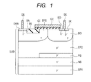
- the semiconductor device mostly has a semiconductor substrate SUB, a p - epitaxial region (first region) EP1, an n + buried region (fifth region) NB, a p + buried region (sixth region) PB, a p - epitaxial region (second region) EP2, an n-type drift region (third region) DRI, a p-type body region (fourth region) BO, an n + drain region (drain region) DRA, an n + source region SO, a gate insulation film GI, a gate electrode layer GE, and an STI structure TR and BI.
- the semiconductor substrate SUB includes silicon for example.
- the semiconductor substrate SUB has a main surface (a plane on the upper side in the figure).
- the p - epitaxial region EP1 is formed in the semiconductor substrate SUB.
- the p - epitaxial region EP2 is formed on the main surface side of the p- epitaxial region EP1 in the semiconductor substrate SUB.
- the n-type drift region DRI is formed on the main surface side of the p - epitaxial region EP2 in the semiconductor substrate SUB.
- the n-type drift region DRI configures a p-n junction extending in the direction along the main surface with the p - epitaxial region EP2.
- the p-type body region BO is formed on the main surface side of the p - epitaxial region EP2 in the semiconductor substrate SUB.
- the p-type body region BO is formed so as to be in contact with the p - epitaxial region EP2, configure a p-n junction with the n-type drift region DRI, and be adjacent to the n-type drift region DRI.
- the p-type body region BO has a p-type impurity concentration higher than that of the p - epitaxial region EP2.
- the STI structure TR and BI has a trench TR and an buried insulation film BI.
- the trench TR is formed in the n-type drift region DRI over the main surface of the semiconductor substrate SUB.
- the buried insulation film BI is formed so as to be buried into the trench TR.
- the n + drain region DRA is formed over the main surface of the semiconductor substrate SUB so as to be in contact with the n-type drift region DRI and has an n-type impurity concentration higher than that of the n-type drift region DRI.
- the n + drain region DRA is located on the side of the STI structure TR and BI opposite to the p-type body region BO and formed so as to be adjacent to the STI structure TR and BI.
- a drain electrode DE is formed over the main surface of the semiconductor substrate SUB so as to be electrically coupled to the n + drain region DRA.
- the n + source region SO is formed over the main surface of the semiconductor substrate SUB so as to configure a p-n junction with the p-type body region BO. Further, a p + impurity region IR which is in contact with the n + source region SO and having a p-type impurity concentration higher than that of the p-type body region BO is formed over the main surface of the semiconductor substrate SUB. A source electrode SE is formed over the main surface of the semiconductor substrate SUB so as to be electrically coupled to both the n + source region SO and the p + impurity region IR.
- the gate electrode layer GE is formed over the p-type body region BO and the n-type drift region DRI interposed between the n + drain region DRA and the n + source region SO through the gate insulation film GI. A part of the gate electrode layer GE hangs over the STI structures TR and BI.
- the n + buried region NB is formed between the p - epitaxial region EP1 and the p- epitaxial region EP2.
- the n + buried region NB is formed so as to configure a p-n junction with the p - epitaxial region EP1 and electrically isolate the p - epitaxial region EP1 from the p - epitaxial region EP2.
- the p + buried region PB is formed between the n + buried region NB and the p- epitaxial region EP2.
- the p + buried region PB has a p-type impurity concentration higher than that of the p - epitaxial region EP2.
- the n + buried region NB configures a p-n junction with the p + buried region PB and also configures a p-n junction with the p - epitaxial region EP2.
- the p + buried region PB is located at least immediately under a junction between the n-type drift region DRI and the p-type body region BO so as to avoid a site immediately under the drain electrode DE. That is, the p + buried region PB is not allocated immediately under the drain electrode DE and the n + buried region NB and the p- epitaxial region EP2 are allocated so as to be in contact with each other. As long as the above conditions are satisfied, the p + buried region PB may be allocated also immediately under the source electrode SE as shown in Fig. 1 for example.
- the LDMOS transistor has an n-type drift region DRI, a p-type body region BO, an n + drain region DRA, an n + source region SO, a gate insulation film GI, and a gate electrode layer GE.
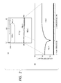
- Fig. 2A shows a diffusion state of impurities in a region in the vicinity of a boundary between a region where a p + buried region PB is allocated so as to be in contact with an n + buried region NB and a region where a p + buried region PB is not allocated particularly in the structure shown in Fig. 1 and Fig. 2B shows a one-dimensional profile of an impurity concentration distribution in the region in the vicinity of the boundary.
- the curved line shown with the solid line in Fig. 2B shows the impurity concentration distribution in the region shown with the dashed-dotted line in Fig. 2A .
- the vertical axis of Fig. 2B represents a logarithmic value of Net Doping and the horizontal axis represents a position in a semiconductor substrate SUB.
- the region where the p + buried region PB is formed has a p-type impurity concentration of about 1x10 16 cm -3 for example. Further, an inflection point where the impurity concentration is very low (about 1x10 14 cm -3 ) in comparison with other regions exists at a boundary between a region where the p + buried region PB is allocated and a region where the p + buried region PB is not allocated.
- a region of a high p-type impurity concentration including the p + buried region PB exists on the right side in the figure and a region of a high n-type impurity concentration caused by the diffusion formed so that an n + buried region NB may build up on the side of the drain electrode DE (on the upper side in the figure) exists on the left side in the figure. Consequently, the curved line of the impurity concentration takes such a shape as shown in the figure.
- the reason why an inflection point having a low impurity concentration appears at a boundary between a region where a p + buried region PB is allocated so as to be in contact with an n + buried region NB and a region where a p + buried region PB is not allocated is that n-type impurities in the n + buried region NB and p-type impurities in the p + buried region PB are compensated with each other.
- the position of an end of a p + buried region PB immediately under a drain region can be identified from the position of the inflection point.
- the inflection point is located on the side of a position immediately under a junction between an n-type drift region DRI and a p-type body region BO rather than a region immediately under a drain region DRA.
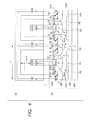
- FIG. 1 An array of LDMOS transistors one of which is shown in Fig. 1 is hereunder explained in reference to Figs. 3A, 3B , 4A, and 4B .
- n + drain region DRA is surrounded by a gate electrode GE over the main surface of a semiconductor substrate SUB and n + source regions SO are allocated on both the sides of the n + drain region DRA.
- the region I surrounded by the dotted line in Figs. 3A and 3B corresponds to the configuration of Fig. 1 .
- n + source regions SO is surrounded by a gate electrode GE and an n + drain region DRA over the main surface of a semiconductor substrate SUB.
- the region I surrounded by the dotted line in Figs. 4A and 4B corresponds to the configuration of Fig. 1 .
- an array is configured by repeating the configuration in the range shown by the pitch P in each of the figures several times in the direction parallel with the main surface.
- a manufacturing method according to the present embodiment is hereunder explained in reference to Figs. 5 to 11 and Fig. 1 .
- a p - epitaxial region EP1 is formed in a semiconductor substrate SUB by epitaxial growth.
- n-type ions are implanted through the surface of the p - epitaxial region EP1 by an ion implantation method.
- an n + buried region NB is formed over the surface of the p - epitaxial region EP1 by applying annealing and diffusing the n-type ions implanted into the p - epitaxial region EP1.
- a photoresist pattern PHR is formed over the surface of the n + buried region NB by an ordinary photoengraving technology.
- p-type ions are implanted through the surface of the n + buried region NB by an ion implantation method with the photoresist pattern PHR as a mask.
- the p-type ions are implanted only in a region RA selectively to the surface of the n + buried region with the photoresist pattern PHR.
- the photoresist PHR is removed by ashing or the like for example.
- a p + buried region PB is formed over the surface of the n + buried region NB by implanting p-type ions or the like. Specifically, a p + buried region PB is not formed in a region RB covered with the photoresist pattern PHR but is formed in the region RA where the photoresist pattern PHR is not formed.
- a p - epitaxial region EP2 is formed over the p + buried region PB and the n + buried region NB by epitaxial growth.
- the p- epitaxial region EP2 is formed so as to surround the side of the p + buried region PB.
- an n-type drift region DRI, a p-type body region BO, an n + drain region DRA, an n + source region SO, a p + impurity region IR, an STI structure TR and BI, a gate insulation film GI, a gate electrode GE, etc. are formed.
- a drain electrode DE and a source electrode SE are formed and a semiconductor device according to the present embodiment shown in Fig. 1 is manufactured.
- Comparative Example 1 shown in Fig. 12 has a configuration formed by omitting an n + buried region NB and a p + buried region PB from the configuration of the present embodiment shown in Fig. 1 .
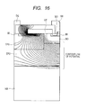
- Comparative Example 1 has a RESURF structure by bringing an n-type drift region DRI into contact with a p - epitaxial region EP from above. Consequently, in the state where a reverse bias is applied to the p - epitaxial region EP and the n-type drift region DRI and breakdown occurs (hereunder referred to merely as a breakdown state), a depletion layer expands in the p - epitaxial region EP under the n-type drift region DRI as shown in Fig.
- a plurality of curved lines shown in Fig. 13 are contour lines of potential (electric potential) in a depletion layer and a plurality of curved lines shown in Fig. 16 are the same.
- a region where contour lines of potential expand means that a depletion layer expands.
- a problem in the configuration of Comparative Example 1 is that a source electrode SE (or a p-type body region BO) is not electrically isolated from a p - epitaxial region EP and hence the configuration is hardly usable as a high-side element.
- a transistor of Comparative Example 1 shown in Fig. 12 when a power supply potential Vdd of 45 V for example is applied to a drain of the transistor TR H , a potential of about 44 V is applied to a source.
- a source electrode SE or a p-type body region BO
- a ground potential (GND) that is the potential of a substrate electrically coupled to the p - epitaxial region EP is destabilized.
- the potential of a source (back gate) that is the ground potential of a low-side element TR L shown in Fig. 14 is also destabilized and the low-side element TR L malfunctions.
- Comparative Example 2 shown in Fig. 15 has a configuration of forming an n + buried region NB as an n-type isolation region.
- a depletion layer formed at a junction between an n + buried region NB and a p- epitaxial region EP2 and a depletion layer formed at a junction between the p - epitaxial region EP2 and an n-type drift region DRI may cause punch through in advance in some cases as shown in Fig. 16 .
- potential difference is caused between the n + buried region NB and an n + source region SO.
- electric field concentration is caused in the vicinity of a junction between a p-type body region BO and the n-type drift region DRI and hence breakdown voltage of Comparative Example 2 is lower than that of Comparative Example 1.
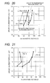
- W DRI (refer to Figs. 3A, 3B and 4A, 4B ) that is the width of a region particularly contributing to electric current between an n + source region SO and an n + drain region DRA in an n-type drift region DRI of Fig. 15 increases, a specific on-resistance increases and an off-breakdown-voltage also increases. That is, they are in the relationship of trade-off.
- an off-breakdown-voltage exceeds a prescribed value (about 90 V for example) however, even though the width of an n-type drift region DRI is expanded, the off-breakdown-voltage does not increase much and the increase of a specific on-resistance comes to be conspicuous. Because the specific on-resistance increases excessively to the off-voltage, the off-breakdown-voltage hardly increases anymore. The reason why an off-breakdown-voltage cannot increase is as follows.
- a depletion layer formed at a junction between an n + buried region NB and a p- epitaxial region EP2 and a depletion layer formed at a junction between the p - epitaxial region EP2 and an n-type drift region DRI may cause punch through in some cases.
- the depletion layers extending in the p - epitaxial region EP2 collide with each other the depletion layers cannot extend anymore and breakdown voltage cannot be increased further.
- the increase of off-breakdown-voltage is suppressed and electric field concentration is caused in the vicinity of a junction between a p-type body region BO and the n-type drift region DRI.
- Comparative Example 3 shown in Fig. 18 has a configuration formed by adding an n + buried region NB similar to Comparative Example 2 in Fig. 15 and a p + buried region PB formed so as to be in contact with the top face of the n + buried region NB to the configuration of Comparative Example 1 shown in Fig. 12 .
- the p + buried region PB has a p-type impurity concentration higher than that of a p - epitaxial region EP2
- a high electric field region is caused in the vicinity of a junction between the p + buried region PB and the n + buried region NB.
- a junction between a p + buried region PB and an n + buried region NB in Fig. 18 shifts to the side lower than a junction between a p - epitaxial region EP2 and an n + buried region NB (to the side of a p - epitaxial region EP1) in Fig. 15 for example. Consequently, a distance allowing a depletion layer caused at a junction between the n + buried region NB and a p - epitaxial region EP2 (p + buried region PB) to extend increases and an off-breakdown-voltage can be increased.
- Fig. 15 Distributions of electric field strengths at breakdown in the structure of Fig. 15 (Comparative Example 2) and the structure of Fig. 18 (Comparative Example 3) are investigated.
- the result in the structure of Fig. 15 is shown in Fig. 19A and the result in the structure of Fig. 18 is shown in Fig. 19B , respectively.
- contour lines of potential at breakdown in the structure of Fig. 15 (Comparative Example 2) and the structure of Fig. 18 (Comparative Example 3) are shown in Figs. 19C and 19D .
- a specific on-resistance in Comparative Example 3 shown in Fig. 18 is about 1.2 m ⁇ cm 2 and decreases by about 30% from about 1.8 m ⁇ cm 2 in Comparative Example 2 shown in Fig. 15 .
- the off-breakdown-voltage is about 92 V in Comparative Example 2 of Fig. 15
- the off-breakdown-voltage is about 97 V in Comparative Example 3 shown in Fig. 18 and increases about 5 V from Comparative Example 2.
- the present inventors have investigated the relationship between an on-breakdown-voltage and a specific on-resistance in the structure of Fig. 15 (Comparative Example 2) and the structure of Fig. 18 (Comparative Example 3). The results are shown in Fig. 21 .
- Fig. 22 the specific on-resistance in the structure showing the results of Fig. 22 is 1.4 m ⁇ cm 2 and the gate voltage in the structure is 5 V.
- the present inventors have comparatively studied the state of applying a high bias to a drain at on-operation in each of the structures of Figs. 15 and 18 .
- a current distribution and impact ionization rates are simulated in an on-state, namely under the condition of a gate voltage of 5 V and a drain voltage Vd of 75 V.
- the results of the impact ionization rates are shown in Figs. 23A and 23B and the current distributions are shown in Figs. 23C and 23D .
- the distributions of hole currents under the condition of the same on-state are shown in Figs. 24A and 24B .
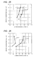
- Figs. 25, 26 , and 27 those are the figures of the cases where corresponding data in the structure of Fig. 1 according to the present embodiment are added to the data shown in Figs. 20, 21 , and 22 , respectively.
- the data added in relation to Fig. 1 are obtained by simulation under the condition of a specific on-resistance of 1.4 m ⁇ cm 2 .
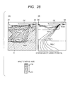
- Fig. 28A Impact ionization rates in an on-state in the structure of Fig. 1 (Embodiment 1) are shown in Fig. 28A and an electric current distribution is shown in Fig. 28B .
- a p - epitaxial region EP1 is electrically isolated from a p - epitaxial region EP2 by an n + buried region NB to which a potential identical to a drain potential is applied, it is possible to reduce malfunctions even when a semiconductor device is used as a high-side element.
- a p + buried region PB coupled to an n + buried region NB is allocated at least immediately under a junction between an n-type drift region DRI and a p-type body region BO.
- the effect of dispersing the concentration of an electric field increases at the junction between the n-type drift region DRI and the p-type body region BO.
- the distance from the junction between the n-type drift region DRI and the p-type body region BO to the p + buried region PB is the shortest. Consequently, by allocating a p + buried region PB immediately under a junction between an n-type drift region DRI and a p-type body region BO, the effect of dispersing a strong electric field strength increases at the junction between the n-type drift region DRI and the p-type body region BO. As a result, the effect of improving the off-breakdown-voltage of a semiconductor device increases.
- a p + buried region PB is not formed so as to be in contact with the whole plane of an n + buried region NB and the p + buried region PB is not allocated immediately under a drain electrode DE.
- the impact ionization rates in the region H in Fig. 28A are lower than those in the region E of Fig. 23B , it is possible to inhibit the impact ionization rates from increasing. This is because, by not allocating a p + buried region PB immediately under a drain electrode DE like Fig.
- a semiconductor device in reference to Fig 30A , basically has a configuration similar to that of Fig. 1 according to Embodiment 1 but further has an n-type region (seventh region) NR.
- An n-type region NR is formed in a semiconductor substrate SUB so as to reach an n + buried region NB from the main surface of the semiconductor substrate SUB.
- the n-type region NR has an n-type diffusion region DNW extending from the main surface side so as to reach the n + buried region NB and an n-type contact region NCR being formed over the main surface and having an n-type impurity concentration higher than that in the n-type diffusion region DNW.
- An electrode DE to which a drain potential is applied is formed over the main surface of the semiconductor substrate SUB so as to be electrically coupled to the n-type contact region NCR. In this way, the n-type region NR and the n + buried region NB are configured so that a drain potential identical to an n + drain region DRA is applied.
- An STI structure TR and BI is formed over the main surface of the semiconductor substrate SUB between the n-type contact region NCR and a p + impurity region IR.
- a p + buried region PB is formed so as not to directly be in contact with the n-type diffusion region DNW by interposing a p - epitaxial region EP2 between the p + buried region PB and the n-type diffusion region DNW.
- the p + buried region PB is formed so as to be in contact with both the n + buried region NB and the p - epitaxial region EP2.
- the curved line shown by the solid line in the figure shows an impurity concentration distribution in the region shown by the dashed-dotted line in Fig. 30A , namely the parts of the p + buried region PB, the p - epitaxial region EP2, and the n-type diffusion region DNW.
- the vertical axis in Fig. 30B represents a logarithmic value of Net Doping and the horizontal axis represents a position (on the dashed-dotted line XXXB-XXXB) in the semiconductor substrate SUB.
- the concentration of p-type impurities in the p + buried region PB is higher than that contained in the p - epitaxial region EP2.
- the p-type impurity concentration in the p + buried region PB is about 1x10 16 cm -3 for example and the p-type impurity concentration in the p - epitaxial region EP2 is 1x10 15 cm -3 for example.
- the array of the LDMOS transistors is basically the same as the array of the first example according to Embodiment 1 shown in Figs. 3A and 3B but, by allocating an n-type diffusion region DNW as shown in the figure, the configuration in the range of the pitch P1 in the figure is repeated in the direction along the main surface.
- Fig. 30A represents a sectional view of the region XXX surrounded by the dotted line in Figs. 31A and 31B .
- an n-type diffusion region DNW is coupled to an n-type drift region DRI and an n + contact region formed on the main surface side of the n-type diffusion region DNW is integrated with an n + drain region DRA.
- the array of the LDMOS transistors of the second example is basically the same as the array of the second example according to Embodiment 1 shown in Figs. 4A and 4B but, by allocating an n-type diffusion region DNW as shown in the figure, the configuration in the range of the pitch P2 in the figure is repeated in the direction along the main surface.
- Fig. 32 represents a sectional view of the region XXXII surrounded by the dotted line in Figs. 33A and 33B .
- an n-type diffusion region DNW can be coupled to an n-type drift region DRI and it is not necessary to install an STI structure TR and BI for electrically separating the n-type diffusion region DNW from a p + impurity region IR unlike the array of the first example shown in Figs. 30A and 30B . Consequently, the pitch P2 in the array of the second example can be smaller than the pitch P1 in the array of the first example. In the array of the first example shown in Figs. 30A and 30B in contrast, since a gate electrode GE is allocated so as to surround the outer circumference of an n + drain region DRA over the main surface, it is possible to inhibit: a depletion layer from expanding outward; and breakdown voltage from decreasing.
- An n-type diffusion region DNW according to the present embodiment may also be formed so as to be in contact with an n + buried region NB by implanting n-type impurities in the vicinity of the main surface of a semiconductor substrate SUB at a high concentration and successively dispersing them through annealing treatment at a high temperature for a long time. Otherwise, an n-type diffusion region DNW may also be formed so as to be in contact with an n + buried region NB by implanting n-type impurities into a deep site of a p - epitaxial region EP2 by high energy implantation and successively dispersing them through annealing treatment.
- an LDMOS transistor like Embodiment 1 is sometimes formed over one chip through a process identical to the process of a CMOS (Complementary MOS), a bipolar transistor, a diode, a memory device, etc.
- CMOS Complementary MOS
- a transistor according to Embodiment 1 is laid out over such a chip, it is necessary to electrically isolate the transistor from other elements.
- a structure for electrical isolation is explained in reference to Figs. 34 and 35 .
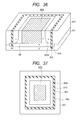
- an n-type diffusion region DNW (seventh region) is formed so as to surround the circumference of a region ARA where an array (lateral elements) in which the layout of LDMOS transistors shown in Figs. 3A and 3B for example is repeated is allocated in a planar view.
- the n-type diffusion region DNW is formed in a semiconductor substrate SUB so as to reach an n + buried region NB from the main surface of the semiconductor substrate SUB in the manner of configuring a p-n junction with a p - epitaxial region EP2.
- the array of LDMOS transistors is electrically isolated from other elements by the n-type diffusion region DNW.
- a potential identical to a drain electrode DE (refer to Figs. 30A and 30B ) is applied to the n-type diffusion region DNW as the isolation region and the n + buried region NB.
- the n-type diffusion region DNW in Figs. 34 and 35 may also be the n-type diffusion region DNW in Figs. 32 , 33A and 33B .
- the array of LDMOS transistors formed inside the n-type diffusion region DNW in Figs. 33A and 33B is electrically isolated from other elements by the n-type diffusion region DNW in Figs. 33A and 33B .
- n-type impurities in an n-type diffusion region DNW diffuse up to an array region ARA of LDMOS transistors, the transistor performance is influenced. Consequently, it is necessary to design the interval X1 between an n-type diffusion region DNW and an array region ARA so as to be a width not influencing transistor performance.
- the interval X1 corresponds to the interval X1 in Figs. 31A and 31B when the n-type diffusion region DNW in Figs. 31A and 31B corresponds to the n-type diffusion region DNW in Fig. 34 for example.
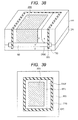
- a trench isolation for electrically isolating an array region ARA of LDMOS transistors from other elements is formed.
- the trench isolation has an isolation trench TRS and a filled insulation layer BIS.
- the isolation trench TRS surrounds the circumference of the array region ARA of LDMOS transistors in a planar view.
- the isolation trench TRS reaches a p - epitaxial region EP1 passing from the main surface of a semiconductor substrate SUB through an n + buried region NB. In this way, it is possible to inhibit electrical coupling between an array region ARA and another element adjacent to the array region for example caused by the n + buried region NB.
- the filled insulation layer BIS is formed so as to fill the interior of the isolation trench TRS.
- a trench isolation is used for electrically isolating an array region ARA from other elements, it is unnecessary to take the influence of the diffusion of n-type impurities on a transistor into consideration unlike the case of installing an n-type diffusion region DNW in Embodiment 3.
- an n-type diffusion region DNW in Embodiment 4 is formed only on one side (on the right side in the figures) of the circumference of a region ARA in a planar view and the other part of the configuration is the same as the configuration of Embodiment 4.
- an array region ARA is electrically isolated from other elements by a trench isolation. Consequently, an n-type diffusion region DNW is formed exclusively for applying a potential identical to a potential applied to a drain electrode DE (refer to Figs. 30A and 30B ) to an n + buried region NB. Consequently, an n-type diffusion region DNW may be formed only at a part of the circumference of an array region ARA on a main surface. In this way, it is possible to: reduce a semiconductor device forming area on a main surface to the extent that the region where an n-type diffusion region DNW is formed reduces; and obtain a chip area reduction effect.
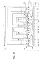
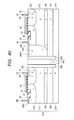
- an LDMOS transistor shown on the left side in Fig. 40 for example as another element electrically isolated from an array region ARA in Embodiments 2 to 5.
- the LDMOS transistor shown on the left side in Fig. 40 has a structure of Comparative Example 3 in Fig. 18 but may also have a structure of Comparative Example 1 in Fig. 12 or Comparative Example 2 in Fig. 15 for example.
- the LDMOS transistor shown on the left side in Fig. 40 is only an example and a diode, an IGBT (Insulated Gate Bipolar Transistor), etc. may be formed.
- the LDMOS transistor shown on the left side in Fig. 40 is formed as a layer identical to the layer of an LDMOS transistor having the structure of Figs. 3A and 3B shown on the right side in Fig. 40 .
- the present invention can be applied to a semiconductor device having a lateral element particularly advantageously.
Landscapes
- Insulated Gate Type Field-Effect Transistor (AREA)
Applications Claiming Priority (1)
| Application Number | Priority Date | Filing Date | Title |
|---|---|---|---|
| JP2011258570A JP5898473B2 (ja) | 2011-11-28 | 2011-11-28 | 半導体装置 |
Publications (2)
| Publication Number | Publication Date |
|---|---|
| EP2597680A2 true EP2597680A2 (de) | 2013-05-29 |
| EP2597680A3 EP2597680A3 (de) | 2013-12-18 |
Family
ID=47594287
Family Applications (1)
| Application Number | Title | Priority Date | Filing Date |
|---|---|---|---|
| EP12193092.9A Withdrawn EP2597680A3 (de) | 2011-11-28 | 2012-11-16 | Halbleiterbauelement |
Country Status (4)
| Country | Link |
|---|---|
| US (2) | US8890243B2 (de) |
| EP (1) | EP2597680A3 (de) |
| JP (1) | JP5898473B2 (de) |
| CN (1) | CN103137703B (de) |
Families Citing this family (18)
| Publication number | Priority date | Publication date | Assignee | Title |
|---|---|---|---|---|
| JP5898473B2 (ja) * | 2011-11-28 | 2016-04-06 | ルネサスエレクトロニクス株式会社 | 半導体装置 |
| US9076863B2 (en) * | 2013-07-17 | 2015-07-07 | Texas Instruments Incorporated | Semiconductor structure with a doped region between two deep trench isolation structures |
| CN104347420B (zh) * | 2013-08-07 | 2018-06-01 | 中芯国际集成电路制造(北京)有限公司 | Ldmos器件及其形成方法 |
| CN104600111A (zh) * | 2013-10-31 | 2015-05-06 | 上海华虹宏力半导体制造有限公司 | Ldmos器件 |
| CN104766885B (zh) * | 2014-01-08 | 2018-04-13 | 无锡华润上华科技有限公司 | 一种对称隔离ldmos器件及其制造方法 |
| US9660074B2 (en) * | 2014-08-07 | 2017-05-23 | Texas Instruments Incorporated | Methods and apparatus for LDMOS devices with cascaded RESURF implants and double buffers |
| JP6509665B2 (ja) * | 2015-07-23 | 2019-05-08 | ルネサスエレクトロニクス株式会社 | 半導体装置 |
| US9911845B2 (en) * | 2015-12-10 | 2018-03-06 | Taiwan Semiconductor Manufacturing Company, Ltd. | High voltage LDMOS transistor and methods for manufacturing the same |
| JP6591312B2 (ja) * | 2016-02-25 | 2019-10-16 | ルネサスエレクトロニクス株式会社 | 半導体装置 |
| CN107146814B (zh) * | 2016-03-01 | 2020-09-11 | 世界先进积体电路股份有限公司 | 高压半导体装置及其制造方法 |
| CN107437563B (zh) * | 2016-05-27 | 2020-03-10 | 中芯国际集成电路制造(上海)有限公司 | Ldmos晶体管及其形成方法、以及esd器件及其形成方法 |
| WO2018074228A1 (ja) * | 2016-10-18 | 2018-04-26 | 株式会社デンソー | 半導体装置およびその製造方法 |
| JP6677672B2 (ja) | 2017-03-24 | 2020-04-08 | 株式会社東芝 | 半導体装置 |
| CN109216453B (zh) * | 2017-07-04 | 2022-02-15 | 世界先进积体电路股份有限公司 | 高压半导体装置及其制造方法 |
| US10128331B1 (en) * | 2017-08-01 | 2018-11-13 | Vanguard International Semiconductor Corporation | High-voltage semiconductor device and method for manufacturing the same |
| JP7195167B2 (ja) * | 2019-02-08 | 2022-12-23 | ルネサスエレクトロニクス株式会社 | 半導体装置及び半導体装置の製造方法 |
| JP7623267B2 (ja) * | 2021-11-05 | 2025-01-28 | ルネサスエレクトロニクス株式会社 | 半導体装置の製造方法 |
| CN116799033A (zh) * | 2023-03-07 | 2023-09-22 | 上海华虹宏力半导体制造有限公司 | 高压ldmos |
Citations (2)
| Publication number | Priority date | Publication date | Assignee | Title |
|---|---|---|---|---|
| US7095092B2 (en) | 2004-04-30 | 2006-08-22 | Freescale Semiconductor, Inc. | Semiconductor device and method of forming the same |
| JP2006237223A (ja) | 2005-02-24 | 2006-09-07 | Sanyo Electric Co Ltd | 半導体装置 |
Family Cites Families (15)
| Publication number | Priority date | Publication date | Assignee | Title |
|---|---|---|---|---|
| US5386136A (en) * | 1991-05-06 | 1995-01-31 | Siliconix Incorporated | Lightly-doped drain MOSFET with improved breakdown characteristics |
| DE10234677A1 (de) * | 2002-07-30 | 2004-02-12 | Infineon Technologies Ag | Feldeffekttransistor, Verfahren zum Herstellen eines Feldeffekttransistors und Verfahren zum Betreiben eines Feldeffekttransistors |
| KR100948139B1 (ko) * | 2003-04-09 | 2010-03-18 | 페어차일드코리아반도체 주식회사 | 높은 브레이크다운 전압 및 낮은 온 저항을 위한 다중전류 이동 경로를 갖는 수평형 이중-확산 모스 트랜지스터 |
| US8253197B2 (en) * | 2004-01-29 | 2012-08-28 | Enpirion, Inc. | Integrated circuit with a laterally diffused metal oxide semiconductor device and method of forming the same |
| US7468537B2 (en) * | 2004-12-15 | 2008-12-23 | Texas Instruments Incorporated | Drain extended PMOS transistors and methods for making the same |
| US7791161B2 (en) * | 2005-08-25 | 2010-09-07 | Freescale Semiconductor, Inc. | Semiconductor devices employing poly-filled trenches |
| US7538396B2 (en) * | 2007-01-19 | 2009-05-26 | Episil Technologies Inc. | Semiconductor device and complementary metal-oxide-semiconductor field effect transistor |
| US20080237702A1 (en) * | 2007-03-26 | 2008-10-02 | Chih-Hua Lee | Ldmos transistor and method of making the same |
| JP4595002B2 (ja) * | 2008-07-09 | 2010-12-08 | 株式会社東芝 | 半導体装置 |
| JP2010245369A (ja) * | 2009-04-08 | 2010-10-28 | Toyota Motor Corp | Ldmosトランジスタ及びその製造方法 |
| JP5534298B2 (ja) * | 2009-06-16 | 2014-06-25 | ルネサスエレクトロニクス株式会社 | 半導体装置 |
| JP5729745B2 (ja) * | 2009-09-15 | 2015-06-03 | ルネサスエレクトロニクス株式会社 | 半導体装置およびその製造方法 |
| JP2011100847A (ja) * | 2009-11-05 | 2011-05-19 | Sharp Corp | 半導体装置及びその製造方法 |
| KR101681494B1 (ko) * | 2010-03-03 | 2016-12-01 | 삼성전자 주식회사 | 반도체 장치 |
| JP5898473B2 (ja) * | 2011-11-28 | 2016-04-06 | ルネサスエレクトロニクス株式会社 | 半導体装置 |
-
2011
- 2011-11-28 JP JP2011258570A patent/JP5898473B2/ja not_active Expired - Fee Related
-
2012
- 2012-11-16 EP EP12193092.9A patent/EP2597680A3/de not_active Withdrawn
- 2012-11-27 US US13/686,900 patent/US8890243B2/en active Active
- 2012-11-28 CN CN201210495284.7A patent/CN103137703B/zh active Active
-
2014
- 2014-10-27 US US14/524,863 patent/US20150145035A1/en not_active Abandoned
Patent Citations (2)
| Publication number | Priority date | Publication date | Assignee | Title |
|---|---|---|---|---|
| US7095092B2 (en) | 2004-04-30 | 2006-08-22 | Freescale Semiconductor, Inc. | Semiconductor device and method of forming the same |
| JP2006237223A (ja) | 2005-02-24 | 2006-09-07 | Sanyo Electric Co Ltd | 半導体装置 |
Non-Patent Citations (1)
| Title |
|---|
| R. ZHU ET AL.: "A 65V, 0.56 m?.cm2 Resurf LDMOS in a 0.35 µm CMOS Process", IEEE ISPSD2000, pages 335 - 338 |
Also Published As
| Publication number | Publication date |
|---|---|
| JP5898473B2 (ja) | 2016-04-06 |
| EP2597680A3 (de) | 2013-12-18 |
| US20150145035A1 (en) | 2015-05-28 |
| JP2013115166A (ja) | 2013-06-10 |
| US20130134510A1 (en) | 2013-05-30 |
| CN103137703B (zh) | 2017-06-09 |
| CN103137703A (zh) | 2013-06-05 |
| US8890243B2 (en) | 2014-11-18 |
Similar Documents
| Publication | Publication Date | Title |
|---|---|---|
| US8890243B2 (en) | Semiconductor device | |
| US10014404B2 (en) | MOS-gated power devices, methods, and integrated circuits | |
| JP5491723B2 (ja) | 電力用半導体装置 | |
| JP6713453B2 (ja) | カスケードされたリサーフ注入及び二重バッファを備えるldmosデバイスのための方法及び装置 | |
| US8866252B2 (en) | Power semiconductor devices and fabrication methods | |
| US8541862B2 (en) | Semiconductor device with self-biased isolation | |
| US10032904B2 (en) | Semiconductor device with non-isolated power transistor with integrated diode protection | |
| KR101941295B1 (ko) | 반도체 소자 | |
| US8791511B2 (en) | Semiconductor device and manufacturing method thereof | |
| US10366981B2 (en) | Power semiconductor devices | |
| WO2006020064A2 (en) | Asymmetric hetero-doped high-voltage mosfet (ah2mos) | |
| US20090321822A1 (en) | High-voltage transistor with improved high stride performance | |
| JP6277785B2 (ja) | 半導体装置 | |
| JP2007042892A (ja) | トレンチ型misfet | |
| US9293525B2 (en) | Semiconductor device and method of manufacturing semiconductor device | |
| JP5038885B2 (ja) | 高電圧pmosトランジスタの製造方法 | |
| KR100825466B1 (ko) | 고전압 nmos 트랜지스터 및 그것의 제조 방법 | |
| KR20110078621A (ko) | 반도체 소자 및 그 제조 방법 | |
| KR20100046354A (ko) | Ldmos 트랜지스터 및 그의 제조 방법 | |
| JP2008060152A (ja) | 半導体装置及びその製造方法 | |
| CN115064586B (zh) | Ldmos器件及其制备方法 | |
| KR20150101043A (ko) | 반도체 소자의 제조 방법 |
Legal Events
| Date | Code | Title | Description |
|---|---|---|---|
| PUAI | Public reference made under article 153(3) epc to a published international application that has entered the european phase |
Free format text: ORIGINAL CODE: 0009012 |
|
| AK | Designated contracting states |
Kind code of ref document: A2 Designated state(s): AL AT BE BG CH CY CZ DE DK EE ES FI FR GB GR HR HU IE IS IT LI LT LU LV MC MK MT NL NO PL PT RO RS SE SI SK SM TR |
|
| AX | Request for extension of the european patent |
Extension state: BA ME |
|
| PUAL | Search report despatched |
Free format text: ORIGINAL CODE: 0009013 |
|
| AK | Designated contracting states |
Kind code of ref document: A3 Designated state(s): AL AT BE BG CH CY CZ DE DK EE ES FI FR GB GR HR HU IE IS IT LI LT LU LV MC MK MT NL NO PL PT RO RS SE SI SK SM TR |
|
| AX | Request for extension of the european patent |
Extension state: BA ME |
|
| RIC1 | Information provided on ipc code assigned before grant |
Ipc: H01L 29/10 20060101ALI20131112BHEP Ipc: H01L 29/78 20060101AFI20131112BHEP Ipc: H01L 29/06 20060101ALI20131112BHEP |
|
| STAA | Information on the status of an ep patent application or granted ep patent |
Free format text: STATUS: THE APPLICATION IS DEEMED TO BE WITHDRAWN |
|
| 18D | Application deemed to be withdrawn |
Effective date: 20140619 |