EP2600399A2 - Leistungshalbleiterbauelement - Google Patents
Leistungshalbleiterbauelement Download PDFInfo
- Publication number
- EP2600399A2 EP2600399A2 EP12195144.6A EP12195144A EP2600399A2 EP 2600399 A2 EP2600399 A2 EP 2600399A2 EP 12195144 A EP12195144 A EP 12195144A EP 2600399 A2 EP2600399 A2 EP 2600399A2
- Authority
- EP
- European Patent Office
- Prior art keywords
- base
- semiconductor device
- power semiconductor
- protruding portion
- set forth
- Prior art date
- Legal status (The legal status is an assumption and is not a legal conclusion. Google has not performed a legal analysis and makes no representation as to the accuracy of the status listed.)
- Granted
Links
Images


Classifications
-
- H—ELECTRICITY
- H10—SEMICONDUCTOR DEVICES; ELECTRIC SOLID-STATE DEVICES NOT OTHERWISE PROVIDED FOR
- H10W—GENERIC PACKAGES, INTERCONNECTIONS, CONNECTORS OR OTHER CONSTRUCTIONAL DETAILS OF DEVICES COVERED BY CLASS H10
- H10W40/00—Arrangements for thermal protection or thermal control
- H10W40/40—Arrangements for thermal protection or thermal control involving heat exchange by flowing fluids
- H10W40/47—Arrangements for thermal protection or thermal control involving heat exchange by flowing fluids by flowing liquids, e.g. forced water cooling
-
- H—ELECTRICITY
- H10—SEMICONDUCTOR DEVICES; ELECTRIC SOLID-STATE DEVICES NOT OTHERWISE PROVIDED FOR
- H10W—GENERIC PACKAGES, INTERCONNECTIONS, CONNECTORS OR OTHER CONSTRUCTIONAL DETAILS OF DEVICES COVERED BY CLASS H10
- H10W40/00—Arrangements for thermal protection or thermal control
-
- H—ELECTRICITY
- H10—SEMICONDUCTOR DEVICES; ELECTRIC SOLID-STATE DEVICES NOT OTHERWISE PROVIDED FOR
- H10W—GENERIC PACKAGES, INTERCONNECTIONS, CONNECTORS OR OTHER CONSTRUCTIONAL DETAILS OF DEVICES COVERED BY CLASS H10
- H10W40/00—Arrangements for thermal protection or thermal control
- H10W40/20—Arrangements for cooling
- H10W40/25—Arrangements for cooling characterised by their materials
- H10W40/255—Arrangements for cooling characterised by their materials having a laminate or multilayered structure, e.g. direct bond copper [DBC] ceramic substrates
-
- H—ELECTRICITY
- H10—SEMICONDUCTOR DEVICES; ELECTRIC SOLID-STATE DEVICES NOT OTHERWISE PROVIDED FOR
- H10W—GENERIC PACKAGES, INTERCONNECTIONS, CONNECTORS OR OTHER CONSTRUCTIONAL DETAILS OF DEVICES COVERED BY CLASS H10
- H10W40/00—Arrangements for thermal protection or thermal control
- H10W40/70—Fillings or auxiliary members in containers or in encapsulations for thermal protection or control
-
- H—ELECTRICITY
- H10—SEMICONDUCTOR DEVICES; ELECTRIC SOLID-STATE DEVICES NOT OTHERWISE PROVIDED FOR
- H10W—GENERIC PACKAGES, INTERCONNECTIONS, CONNECTORS OR OTHER CONSTRUCTIONAL DETAILS OF DEVICES COVERED BY CLASS H10
- H10W42/00—Arrangements for protection of devices
- H10W42/121—Arrangements for protection of devices protecting against mechanical damage
-
- H—ELECTRICITY
- H10—SEMICONDUCTOR DEVICES; ELECTRIC SOLID-STATE DEVICES NOT OTHERWISE PROVIDED FOR
- H10W—GENERIC PACKAGES, INTERCONNECTIONS, CONNECTORS OR OTHER CONSTRUCTIONAL DETAILS OF DEVICES COVERED BY CLASS H10
- H10W76/00—Containers; Fillings or auxiliary members therefor; Seals
- H10W76/40—Fillings or auxiliary members in containers, e.g. centering rings
- H10W76/42—Fillings
- H10W76/47—Solid or gel fillings
-
- H—ELECTRICITY
- H10—SEMICONDUCTOR DEVICES; ELECTRIC SOLID-STATE DEVICES NOT OTHERWISE PROVIDED FOR
- H10W—GENERIC PACKAGES, INTERCONNECTIONS, CONNECTORS OR OTHER CONSTRUCTIONAL DETAILS OF DEVICES COVERED BY CLASS H10
- H10W72/00—Interconnections or connectors in packages
- H10W72/851—Dispositions of multiple connectors or interconnections
- H10W72/874—On different surfaces
- H10W72/884—Die-attach connectors and bond wires
-
- H—ELECTRICITY
- H10—SEMICONDUCTOR DEVICES; ELECTRIC SOLID-STATE DEVICES NOT OTHERWISE PROVIDED FOR
- H10W—GENERIC PACKAGES, INTERCONNECTIONS, CONNECTORS OR OTHER CONSTRUCTIONAL DETAILS OF DEVICES COVERED BY CLASS H10
- H10W90/00—Package configurations
- H10W90/701—Package configurations characterised by the relative positions of pads or connectors relative to package parts
- H10W90/751—Package configurations characterised by the relative positions of pads or connectors relative to package parts of bond wires
- H10W90/753—Package configurations characterised by the relative positions of pads or connectors relative to package parts of bond wires between laterally-adjacent chips
Definitions
- the present invention relates to a power semiconductor device.
- a power semiconductor device including a power semiconductor circuit is used for controlling electrical apparatus such as high output motors and generators, and for power conversion.
- a power semiconductor device is, for example, an IGBT (Insulated Gate Bipolar Transistor).
- One way to obtain a lightweight power semiconductor device is to reduce a thickness of a base (substrate) constituting the power semiconductor device.
- a base substrate
- connection portions such as a solder to fix the base to individual members may crack by fatigue through expanding and shrinking of the base. As a consequence, the connection portions of the semiconductor device may easily be damaged, and it is difficult to use the semiconductor device for a long period of time in some cases. This means that a lifetime of the power semiconductor device becomes short.
- a purpose of the present invention is to provide a power semiconductor device which has a light weight, a high heat dissipation efficiency, and a high rigidity.
- a power semiconductor device which has a light weight, high heat dissipation efficiency, and high rigidity can be provided.
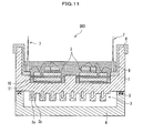
- a power semiconductor device 100 As shown in FIG. 1 , a power semiconductor device 100 according to a first embodiment is provided with a base 1, semiconductor circuits 2 which are arranged on the base 1, and a cooling fin 3 which cools the semiconductor circuits 2.
- the base 1 has an edge portion 1a surrounding a periphery thereof, a protruding portion 1b which is formed by bridging the edge portion 1a inside a space formed by being surrounded with the edge portion 1a, and a bottom portion 1c on which the protruding portion 1b is formed.
- the edge portion 1a is one form of the "protruding portions" defined in claims. Therefore, in the present embodiment, there are two or more "protruding portions” defined in claims. Details of the edge portion 1a, the protruding portion 1b, and the bottom portion 1c will be described later with reference to FIG. 2A .
- the power semiconductor device 100 is further provided with a cooling jacket 4, a seal member 5, a block 6, electrodes 7, and wirings 2f.
- a silicone gel 9 is filled in the base 1, and thus the semiconductor circuits 2 are sealed.
- a refrigerant (not shown) flows through a space which is formed between the base 1 and the cooling jacket 4.
- the base 1 is a member made of aluminum. Plating with nickel or the like is applied to a surface of the base 1, although not shown. In this manner, it is possible to improve a corrosion resistance as well as connectivity (fixing strength) of the semiconductor circuit 2 described later.
- the base 1 has the edge portion 1a, the protruding portion 1b, and the bottom portion 1c, as shown in the above FIGS. 1 and 2 .
- the edge portion 1a and the protruding portion 1b have respective predetermined heights and widths independently.
- the power semiconductor device 100 is formed with the edge portion 1a and the protruding portion 1b on an upper surface 1A of the bottom portion 1c.
- the term “height” is a length in a direction perpendicular to the bottom portion 1c of the base 1.
- the term “width” is a length in a direction parallel to the bottom portion 1c of the base 1.
- a width of the protruding portion 1b is denoted by "W”.
- a thickness of the bottom portion 1c of the base 1 is denoted by "T”.
- a distance between adjacent pin fins 3a is denoted by "L”.
- the width "W” and the thickness “T” are denoted as described above, the width "W” is longer than the thickness "T".
- the rigidity of the base 1 can be increased while a thickness of the bottom portion 1c of the base 1 is reduced.
- a weight of the power semiconductor device 100 can be decreased because the thickness of the bottom portion 1c is reduced.
- the base of a conventional power semiconductor device which has a cooling mechanism cooled by the refrigerant or the like is usually made of a copper. It is because there is a problem that when aluminum or the like is used for the base, a thermal resistance of the base is increased and the semiconductor circuit becomes difficult to be cooled. In other words, it is because heat transfer from the semiconductor circuit to the cooling unit (such as cooling fin) is difficult to be performed and thus the heat dissipation efficiency is decreased.
- the power semiconductor device 100 is used as a material which constitutes the base 1.
- the power semiconductor device 100 is provided with the protruding portion 1b.
- the base 1 By setting as described above the relationship between the width "W" of the protruding portion 1b and the thickness "T" of the bottom portion 1c of the base 1, it is possible to form the base 1 having a thickness which is not conventionally achieved with copper. Therefore, the thickness of the base 1 can be reduced, thereby suppressing an increase of a thermal resistance to the cooling fin 3 from the semiconductor circuit 2. As a consequence, the high heat dissipation efficiency can be maintained even if aluminum is used as the material of the base 1.
- the high rigidity of the power semiconductor device 100 can be maintained even if the thickness of the base 1 is reduced. Furthermore, the weight of the power semiconductor device 100 can be reduced because the thickness of the base 1 is reduced. In addition, since the thickness of the base 1 is reduced, an amount of the thermal expansion of the base 1 can be decreased, thereby suppressing a warpage of the base 1 caused by an ununiformity of the temperature. As a result, the junction portion by the solder can be prevented from being deteriorated, as well as the refrigerant can be prevented from leaking.
- the width "W” and the thickness "T" there is no particular limitation to a specific numerical range of the width "W” and the thickness "T".
- the width "W” can be more than 2 millimeters and not more than 10 millimeters and the thickness "T" can be less than or equal to 2 millimeters.
- a height (including the thickness of the bottom portion 1c) of the edge portion 1a can be 15 millimeters.
- a shortest distance "L” among distances between adjacent pin fins 3a is shorter than the width "W" of the protruding portion 1b. The reason why the power semiconductor device 100 is configured in this manner will be explained.
- the width "W" and the shortest distance "L” satisfy the above relationship.
- the distances between adjacent pin fins 3a can be made short.
- the cooling fin 3 there is no particular limitation to specific numerical values for the cooling fin 3.
- the height of the pin fins 3a can be 6 millimeters and the shortest length "L" can be 1 millimeter.
- the distance between adjacent pin fins 3a is too long, the number of the pin fins 3a is too small, and the heat dissipation efficiency may be decreased.
- the shortest distance "L" is preferably at least about 1 millimeter.
- the semiconductor circuit 2 constitutes a circuit group to function as the power semiconductor device 100. More specifically, the semiconductor circuit 2 includes IGBT elements 2a, diode elements 2b, solders 2c under the elements, substrate top surface conductive layers 2d, and insulating substrates 2e. The semiconductor circuits 2 are electrically connected to the electrodes 7 through the wirings 2f. The IGBT elements 2a and the diode elements 2b are electrically connected with each other through the wirings 2f. And, the diode elements 2b are also electrically connected to the substrate top surface conductive layers 2d through the wirings 2f.
- the semiconductor circuit 2 is located between the edge portion 1a and the protruding portion 1b, and secured to the upper surface (circuit connection surface) 1A of the bottom portion 1c of the base 1.
- the semiconductor circuit 2 is secured to the upper surface 1A (i.e., base 1) through a substrate bottom surface conductive layer 10 and a under substrate solder 11.
- the insulating substrates 2e having an excellent thermal conductivity are used. More specifically, as materials of which the insulating substrates 2e is made, for example, ceramics such as silicon nitride, aluminum nitride, and alumina are used. By the insulating substrates 2e made of such materials, heat from the IGBT elements 2a can be efficiently discharged to the outside of the semiconductor circuit 2.
- the cooling fin 3 is a member which cools the semiconductor circuit 2.
- the IGBT element 2a is used for a switching use
- the diode element 2b is used for a rectifying use.
- a size of each member constituting the semiconductor device 100 is as follows. That is, the insulating substrate 2e has a length of 50 millimeters in the lateral direction on the sheet of FIG. 1 , a length of 30 millimeters in the perpendicular direction to the sheet of FIG. 1 , and a thickness of 0.3 millimeters. Lengths of the substrate top surface conductive layer 2d and the substrate bottom surface conductive layer 10 are all the same, and the length in the lateral direction on the sheet of FIG. 1 is 48 millimeters, the length in the perpendicular direction to the sheet of FIG. 1 is 28 millimeters, and the thickness is 0.5 millimeters.
- the substrate top surface conductive layers 2d are shown as separate members in FIG. 1 , but the above lengths are lengths when they are considered as an integral product. That is, a length from the left end of the substrate top surface conductive layer 2d to the right end of the substrate top surface conductive layer 2d in FIG. 1 is 48 millimeters.
- the length of the IGBT element 2a in the lateral direction on the sheet of FIG. 1 is 10 millimeters, and the length of the diode element 2b in the lateral direction on the sheet of FIG. 1 is 6 millimeters.
- the length in the perpendicular direction to the sheet of FIG. 1 and the thickness are common to the both elements, and the length in the perpendicular direction to the sheet of FIG. 1 is 10 millimeters and the thickness is 0.1 millimeter.
- the length of the insulating substrate 2e in the lateral direction on the sheet of FIG. 1 is longer than the lengths of the substrate top surface conductive layer 2d and the substrate bottom surface conductive layer 10 in the lateral direction on the sheet of FIG. 1 . Therefore, even if side surfaces of the semiconductor circuit 2 are brought into contact with the edge portion 1a or the protruding portion 1b, the insulating substrate 2e is adapted to be in contact with the edge portion 1a or the protruding portion 1b. As a consequence, electrical insulation between the base 1 and the semiconductor circuit 2 can be maintained.
- the cooling fin 3 is, as shown in FIG. 1 , formed on one side of the base 1 opposite to a surface on which the semiconductor circuit 2 is arranged.
- the cooling fin 3 is formed integrally with the base 1. They may be formed separately to be subsequently joined together, but detailed information on this point will be described later.
- the cooling fin 3 is constituted by a plurality of pin fins 3a.
- the same material with base 1 is used. This means that the material constituting the cooling fin 3 in the present invention is aluminum.
- the refrigerant flows through the space which is formed between the base 1 and the cooling jacket 4 (described later), and the refrigerant and the cooling fin 3 are in contact with each other. In this manner, the heat is transferred to the refrigerant from the cooling fin 3, and the semiconductor circuit 2 is cooled.
- the base 1 and the cooling fin 3 are made of aluminum.
- Aluminum is excellent in moldability and workability as compared to copper. Therefore, by constituting the base 1 and the cooling fin 3 by aluminum, they can be integrally formed as in the present embodiment. By the fact that they can be formed integrally, it can be realized that the manufacturing process is simplified and the manufacturing cost is reduced. Such an integral forming can be carried out by forging, for example.
- a portion of the base 1 is forged to form only the cooling fin 3 at first, and the base 1 portion may be cut out by machining.
- the base 1 and the cooling fin 3 may be joined by brazing together after forged separately. In this manner, since the surface of the cooling fin 3 is not required to be formed during forging the base 1, there is an advantage that the forging is easy.
- the cooling jacket 4 is secured to the base 1 by fastening bolts not shown.
- the refrigerant such as water flows through a space which is formed by the cooling jacket 4 and the base 1.
- a seal member 5 such as an O-ring is provided between connection surfaces of the base 1 and the cooling jacket 4. As a consequence, a leakage of the refrigerant is prevented.
- a block 6 is configured to electrically insulate the base 1 from an electrode 7 described later.
- the block 6 is an insulating member disposed between the base 1 and the electrode 7.
- a member including a resin is used in the present embodiment.
- the resin a PBT (PolyButylene Terephthalate), a PPS (PolyPhenylene Sulfide) and the like are listed.
- the electrodes 7 are connection terminals which are connected to the semiconductor circuits 2 through wirings (electrical signal lines) 2f, and are connected to an external device not shown.
- the silicone gel 9 is filled in a space which is formed by being surrounded with the edge portion 1a of the base 1. As shown in FIG. 1 , a height of the edge portion 1a is higher than that of the silicone gel 9. Therefore, a leakage of the silicone gel 9 is prevented. On the other hand, the height of the silicone gel 9 is higher than that of the semiconductor circuit 2. Therefore, the semiconductor circuit 2 is encapsulated by the silicone gel 9. In this manner, the semiconductor circuit 2 is protected from an external atmosphere such as moisture and dust.
- a cover member made of the resin is arranged so as to cover the entire upper surface of the silicone gel 9. By the cover member, an inside of the power semiconductor device 100 is protected from the external atmosphere.
- the IGBT element 2a and the diode element 2b While the power semiconductor device 100 is in operation, the IGBT element 2a and the diode element 2b generate especially a large amount of Joule heat. In order to cool the power semiconductor device 100, it is important to transmit the Joule heat generated from the IGBT element 2a and the diode element 2b to the lower surface of the base 1 with as small a loss as possible, and to dissipate the heat to the refrigerant. Taking this heat dissipation into account, the thickness of the bottom portion 1c of the base 1 in the power semiconductor device 100 is thinner than the thickness (height) of the edge portion 1a. For this reason, the power semiconductor device 100 has a small loss of heat conduction and high heat dissipation efficiency.
- the temperature of power semiconductor device 100 becomes high during operation as described above. Therefore, a large thermal stress is applied to members from each other members having different coefficient of thermal expansion.
- the coefficient of thermal expansion of the insulating substrate 2d is about 2.5 ppm/K if it is made of silicon nitride, and is about 7.1 ppm/K if it is made of alumina.
- the coefficient of thermal expansion of the base 1 is about 24.0 ppm/K if it is made of aluminum. In this manner, the coefficient of thermal expansion of the insulating substrate 2d and that of the base 1 are very different from each other.
- the under substrate solder 11 which is a member connecting the insulating substrate 2d and the base 1 with each other, may be cracked by the thermal fatigue. Therefore, ensuring a thermal fatigue life of the under substrate solder 11 is a major issue.
- the present invention has been devised. As described above, since the thickness of the bottom portion 1c of the base 1 is reduced in the power semiconductor device 100, the thermal expansion at a part of the base 1 to which the under substrate solder 11 is secured is reduced. As a result, the reduction of fatigue lifetime of the under substrate solder 11 can be suppressed.
- the refrigerant flows through on a lower portion (a side to which the cooling jacket 4 is secured) of the base 1. Therefore, a pressure of the refrigerant is applied to the lower portion of the base 1. If the warpage deformation of the base 1 is increased by the pressure, the refrigerant flowing through on the lower portion of the base 1 may be leaked to the outside. Therefore, it is also an important issue to maintain a high rigidity of the base 1 while the thickness of the base 1 is reduced.
- the base 1 is formed with the protruding portion 1b. In this manner, the rigidity of the entire base 1 can be increased while the thickness of the bottom portion of the bases 1 is reduced.
- the high rigidity of the base 1 is further increased by the edge portion 1a.
- the power semiconductor device 100 has the protruding portion 1b formed near a center of the base 1 (see FIGS. 1 and 2 ). Therefore, two regions formed between the protruding portion 1b and the two opposed edge portions 1a have substantially the same area. As a consequence, the two semiconductor circuits 2 can be respectively secured to the two regions by setting the semiconductor circuit 2 to about the size of the area.
- the semiconductor circuits 2 can be respectively fitted into the regions (concaves) which are formed by the edge portion 1a and the protruding portion 1b, during production of the power semiconductor device 100. In this manner, it is not necessary to perform a complicated positioning of the semiconductor circuit 2. As a result, there is no need to prepare and set jigs and tools for positioning separately at the time of soldering, thereby reducing the production cost and the production time.
- a model member 150 as shown in FIG. 3A is prepared in order to confirm the effects by the power semiconductor circuit 100.
- a cross-sectional view taken along a line A-A in FIG. 3A is shown in FIG. 3B .
- the model member 150 includes substrates 20 for elements, under element solders 21, a substrate top surface conductive layer 22, an insulating substrate 23, a substrate bottom surface conductive layer 24, an under substrate solder 25, and a base 26.
- the substrate 20 for elements corresponds to the IGBT element 2a and the diode element 2b shown in FIG. 1 .
- the under element solder 21 corresponds to the solder 2c under the elements
- the substrate top surface conductive layer 22 corresponds to the substrate top surface conductive layer 2d
- the insulating substrate 23 corresponds to the insulating substrate 2e
- the substrate bottom surface conductive layer 24 corresponds to the substrate bottom surface conductive layer 10
- the under substrate solder 25 corresponds to the under substrate solder 11
- the base 26 corresponds to the bottom portion 1c of the base 1, respectively shown in FIG. 1 .
- the effect of reducing the thermal resistance of the power semiconductor device 100 has been evaluated by using the model member 150.
- the result is shown in FIG. 4 .
- the horizontal axis of FIG. 4 stands for a thickness of the base 26 (vertical thickness in FIG. 3B ).
- the vertical axis stands for a normalized value (thermal resistance ratio) when assuming the thermal resistance as 1 (plot R0) in the case where copper base (conventional base) with 3 millimeters thickness is used.
- Measurement of the thermal resistance of the model member 150 has been carried out by performing a heat transfer analysis under a condition that an upper surface of the substrate 20 for the elements is kept at 150 °C and the heat is dissipated from a lower surface of the base 26. In other words, the thermal resistance between the substrate 20 for the elements and the lower surface of the base 26 has been measured.
- the thermal conductivity of aluminum is about 240 W/mK.
- the thermal conductivity of copper is about 390W/mK. Accordingly, the thermal conductivity of copper is 1.6 times as large as compared to the thermal conductivity of aluminum.
- the thermal resistance was increased by 11 % (plot R 1 ) when aluminum base 26 with 3 millimeters thickness same as the copper base was used. However, the thermal resistance was decreased by reducing the thickness of the base 26. More specifically, the thermal resistance was decreased by 4 % (plot R 2 ) compared to the copper base with 3 millimeters thickness when the thickness of the base 26 is reduced to 2 millimeters. The thermal resistance was decreased by 21 % (plot R 3 ) compared to the copper base with 3 millimeters thickness when the thickness of the base 26 is reduced to 1 millimeter. Incidentally, the thermal resistance was same as that of the copper base when the thickness of the base 26 is 2.3 millimeters.
- the base 26 can have an excellent thermal resistance value by reducing the thickness compared to the conventional copper base.
- the power semiconductor device according to the present invention can have excellent heat dissipation efficiency while the weight thereof is reduced compared with the conventional power semiconductor device.
- FIG. 5 shows a deformed shape of the model member 150 at -40 °C with an amount of deformation enlarged by ten times larger than the actual deformation when the temperature of the entire model member 150 was changed from 125 °C to -40 °C.
- the amount of deformation was calculated by the thermal stress analysis using the finite element method over the temperature range of 125 °C to -40 °C.
- FIG. 1 shows a relationship between the thickness of the base 26 and the fatigue life of the under substrate solder 25.
- FIG. 6 shows normalized values (lifetime ratio) when assuming the lifetime of the solder as 1 in the case where the thickness of the base is 3 millimeters.
- the lifetime is converted from plastic strain of the under substrate solder 25 which is obtained from the results of the thermal stress analysis in FIG. 5 .
- the base is made of aluminum.
- the lifetime of the under substrate solder 25 has become longer by 18 % when the thickness of the base 26 is 2 millimeters as compared with the case of 3 millimeters.
- the lifetime of the under substrate solder 25 has become longer by 61 % when the thickness of the base 26 is 1 millimeter as compared with the case of 3 millimeters. In this manner, the lifetime of the solder is made longer by reducing the thickness of the base 26.
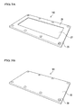
- FIG. 7A shows a model member 160 formed with a protruding portion 28 on edges of the base 27, i.e., a model member 160 provided with a protruding portion 28 in the vicinity of four edges of a rectangular plate.
- FIG. 7B shows a model member 161 formed without a protruding portion. In any of the model member 160 and the model member 161, bolt bores 29 through which the cooling fin is secured, are also shown.
- the thickness of the base As described above, by reducing the thickness of the base, the increase of the thermal resistance can be suppressed, and thus the reduction of the lifetime of the solder can be suppressed, even if the aluminum base is used.
- a base 30 is configured without a protruding portion such as the model member 161 shown in FIG. 7B , the rigidity of the base 30 is reduced when the thickness thereof is simply reduced. It is particularly important to ensure the sufficient rigidity of the base 1 in the power semiconductor device 100, since the pressure of the refrigerant is applied to the lower surface of the base 1, as described above. Therefore, by providing the protruding portions 1b and 28 as shown in FIGS. 1 and 7A , the warpage of the bases 1, 27 by the refrigerant pressure can be suppressed, and thus the leakage of the refrigerant can be prevented.
- FIG. 8 is a graph showing the maximum warpage amount at the edge portion 28 of the base 27, compared with a result of the model member 161 using the conventional copper base with 3 millimeters thickness.
- the maximum warpage amount was calculated by carrying out the finite element analysis when water pressure is applied to the lower surface of the base 27, 30 of the model member 160, 161 shown in FIGS. 7A, 7B .
- the vertical axis stands for normalized value (warpage amount ratio) when assuming the warpage amount of the copper base as 1 in the case where the thickness thereof is 3 millimeters.
- the result of the model member 161 using the conventional copper base with 3 millimeters thickness is also shown (plot W 0 ).
- the warpage amount ratio (1.1) when the thickness of the base 27 is 2 millimeters and the thickness of the protruding portion 28 is 4 millimeters is indicated by a one-dot chain line A.
- the warpage amount ratio (0.67) when the thickness of the base 27 is 2 millimeters and the thickness of the protruding portion 28 is 5 millimeters is indicated by a one-dot chain line B.
- the model member 160 made of aluminum with the protruding portion 28 of 4 millimeters thickness and with the base 27 of 2 millimeters thickness is used (one-dot chain line A)
- the increase of the warpage amount ratio was suppressed to 10 %.
- the warpage amount was not excessively increased even if the aluminum base with 2 millimeters thickness was used instead of the conventional copper base with 3 millimeters thickness.
- the thickness of the protruding portion 28 was set to 5 millimeters, the warpage amount was decreased by 33 %. This means that the warpage amount can be maintained to the same extent as the conventional base, or can be significantly decreased compared to the conventional base, while the thickness of the base can be reduced compared to the conventional copper base by forming the protruding portion 28 on the base.
- the base 1 including the cooling fin 3 is manufactured by forging or other methods, as described above. Then, the blocks 6 made of the resin are fitted into the edge portion 1a of the manufactured base 1 to be in close contact with inner walls of the base 1 ( FIG. 9A ). Securing the blocks 6 to the edge portions 1a is performed by bolts, adhesives and the like. In addition, the electrode 7 is embedded into the block 6 to be secured to the block 6 when the block 6 is molded.
- members into which the semiconductor circuit 2 and the substrate bottom surface conductive layer 10 are formed together are respectively secured to the bottom surface 1A of the base 1 through the under substrate solder 11 ( FIG. 9B ).
- the securing method is performed as follows.
- the under substrate solder 11 is mounted on the bottom surface 1A of the base 1, and then the members into which the semiconductor circuit 2 and the substrate bottom surface conductive layer 10 are formed together are respectively mounted on the solder 11. Then, by heating the whole members in a high temperature furnace, the semiconductor circuit 2 and the substrate bottom surface conductive layer 10 are secured (connected) to the base 1 by the under substrate solder 11.
- the under substrate solder 11 melts when it is heated in the high temperature furnace. However, the molten solder does not leak to the outside of the base 1 because the edge portion 1a has the base 1. As described above, the positioning of the semiconductor circuit 2 is not required during installation, since the placement of the semiconductor circuit 2 is predetermined by the edge portion 1a and the protruding portion 1b. Therefore, the separate jigs and tools for the positioning are not required.
- Each of the semiconductor circuits 2 is secured to the base 1 by the under substrate solder 11, and then the semiconductor circuit 2 and the electrode 7 are electrically connected with each other by the wiring 2f (see FIG. 9C ).
- the silicone gel 9 is injected into the space enclosed by the edge portion 1a ( FIG. 9C ).
- the semiconductor circuit 2 is sealed by the silicone gel 9.
- a cover member made of the resin is attached so as to cover the upper surface of the silicone gel 9.
- the seal member 5 is interposed between the base 1 and the cooling jacket 4, and in this state the cooling jacket 4 is secured by the bolts (not shown) to the base 1 ( FIG. 9D ).
- the power semiconductor device 100 is manufactured by having the refrigerant flow thorough the space formed between the base 1 and the cooling jacket 4.
- the production method of the power semiconductor device 100 is not limited to the above description. Therefore, the power semiconductor device 100 can be manufactured by the methods suitably changed.
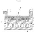
- a power semiconductor device 200 according to a second embodiment will be explained with reference to FIG. 10 .
- the same members as those of the power semiconductor device 100 shown in FIG. 1 are denoted by the same reference signs, and the detailed explanation thereof will be omitted.
- the height of the protruding portion 1b in the power semiconductor device 100 is about the same as the height of the edge portion 1a.
- the power semiconductor device 100 has one space which is formed by being surrounded with the edge portion 1a only.
- the power semiconductor device 200 has two spaces which are formed by partitioning with the protruding portion 1b the space which is formed by being surrounded with the edge portion 1a.
- both of the heights of the edge portion 1a and the protruding portion 1b can be higher than the height of the silicone gel 9.
- the power semiconductor device 200 can be also manufactured similarly to the power semiconductor device 100 by configuring the power semiconductor device 200 in this manner.
- the block 6 and the electrode 7 are newly provided adjacent to the protruding portion 1b. Therefore, the number of the electrodes 7 can be increased as compared with the power semiconductor device 100.
- a power semiconductor device 300 according to a third embodiment will be explained with reference to FIG. 11 .
- the same members as those of the power semiconductor device 100 shown in FIG. 1 are denoted by the same reference signs, and the detailed explanation thereof will be omitted.
- the shape of the cooling fin 3 is different from the shape of the cooling fin 3 of the power semiconductor device 100.
- the cooling fin 3 in the power semiconductor device 300 is constituted by rectangular (plate-like) fins 3b having gaps 3c.
- the refrigerant can also flow through the gaps 3c. Therefore, the contact area of the refrigerant for the rectangular fins 3b becomes large, and thus the heat dissipation efficiency by the cooling fin 3 can be further improved.
- a power semiconductor device 400 according to a fourth embodiment will be explained with reference to FIG. 12 .
- the same members as those of the power semiconductor device 100 shown in FIG. 1 are denoted by the same reference signs, and the detailed explanation thereof will be omitted.
- the substrate bottom surface conductive layer 10 and the under substrate solder 11 provided on the power semiconductor device 100 are removed.
- the insulating substrate 2e is directly secured to the bottom surface 1A without solder.
- Securing the insulating substrate 2e to the base 1 is carried out by the molten metal bonding method. More specifically, the base 1 is formed by forging, and by contacting the insulating substrate 2e with the base 1 in the middle of cooling (before aluminum is completely solidified) after forging, the insulating substrate 2e can be secured to the base 1. At this time, an alloy layer is formed at the interface between the base 1 and the insulating substrate 2e, so that the insulating substrate 2e is directly secured to the base 1.
- the substrate bottom surface conductive layer 10 and the under substrate solder 11 are not required to be provided. For this reason, the heat of the semiconductor circuit 2 can be efficiently transferred to the cooling fin 3 because the thermal resistance is smaller than that of the power semiconductor device 100. In addition, there is an advantage that the above fatigue of the solder is not a problem because the under substrate solder 11 is not provided.
- edge portion 1a and the protruding portion 1b are provided in each of the above embodiments, only the protruding portion 1b can be provided without the edge portion 1a. Furthermore, only the edge portion 1a can be provided without the protruding portion 1b. In this case, the edge portion 1a corresponds to the "protruding portion" specified in claims.
- the location of the protruding portion 1b is not particularly limited, and may be anywhere. However, it is preferable to provide the protruding portion so as to bridge the opposing edges of the base in view of maximizing the effect of the present invention. In the case of the rectangular base, for example, the protruding portion can be provided so as to bridge the opposing corners among four corners.
- the height of the protruding portion 1b can be higher than the height of the edge portion 1a.
- the number of the protruding portion 1b is not limited to one, and may be plural. With the above configurations, the effect of the present invention can be also achieved.
- the material constituting the base 1 is not limited to single aluminum, and may be any material containing aluminum such as aluminum alloy, insulator coated with aluminum, and the like.
- the configuration of the cooling fin 3 is not limited to the above embodiments, and the cooling fin 3 may be in any shape as long as the heat dissipation is efficiently carried out.
- the arrangement of the pin fins 3a is not particularly limited. Taking into account the suitable shortest distance "L”, the pin fins 3a may be appropriately designed and arranged.
- the configuration of the semiconductor circuit 2 is not limited to the above embodiments, and any semiconductor circuit may be similarly applied. Also, the number of the electrodes 7 may be arbitrarily set.
- the kind of the seal member 5 is not limited to the O-ring, and the seal member 5 may be appropriately changed to a packing or the like.
- the gel which seals the semiconductor circuit 2 is not limited to the silicone gel 9, and any insulating gel may be used.
Landscapes
- Cooling Or The Like Of Semiconductors Or Solid State Devices (AREA)
Applications Claiming Priority (1)
| Application Number | Priority Date | Filing Date | Title |
|---|---|---|---|
| JP2011261502A JP5588956B2 (ja) | 2011-11-30 | 2011-11-30 | パワー半導体装置 |
Publications (3)
| Publication Number | Publication Date |
|---|---|
| EP2600399A2 true EP2600399A2 (de) | 2013-06-05 |
| EP2600399A3 EP2600399A3 (de) | 2017-08-09 |
| EP2600399B1 EP2600399B1 (de) | 2021-09-08 |
Family
ID=47522295
Family Applications (1)
| Application Number | Title | Priority Date | Filing Date |
|---|---|---|---|
| EP12195144.6A Active EP2600399B1 (de) | 2011-11-30 | 2012-11-30 | Leistungshalbleiterbauelement |
Country Status (4)
| Country | Link |
|---|---|
| US (1) | US9013877B2 (de) |
| EP (1) | EP2600399B1 (de) |
| JP (1) | JP5588956B2 (de) |
| CN (1) | CN103137576B (de) |
Cited By (3)
| Publication number | Priority date | Publication date | Assignee | Title |
|---|---|---|---|---|
| EP4099375A4 (de) * | 2020-01-28 | 2024-02-21 | Kyocera Corporation | Montagegehäuse für elektronische komponenten und elektronische vorrichtung |
| US12506043B2 (en) | 2021-08-27 | 2025-12-23 | Fuji Electric Co., Ltd. | Semiconductor device |
| WO2026013094A1 (de) * | 2024-07-10 | 2026-01-15 | Zf Friedrichshafen Ag | Elektronische schaltung, verfahren und steuervorrichtung zum betreiben einer elektronischen schaltung |
Families Citing this family (44)
| Publication number | Priority date | Publication date | Assignee | Title |
|---|---|---|---|---|
| JP6138500B2 (ja) * | 2013-01-30 | 2017-05-31 | 株式会社 日立パワーデバイス | パワー半導体装置 |
| KR101407194B1 (ko) * | 2013-05-10 | 2014-06-12 | 현대오트론 주식회사 | 차량의 전자제어장치 |
| JP2015002305A (ja) * | 2013-06-18 | 2015-01-05 | 三菱電機株式会社 | 半導体装置 |
| CN103414356A (zh) * | 2013-08-16 | 2013-11-27 | 张晓民 | 共单极悬浮式整流模块 |
| JP6020731B2 (ja) * | 2013-08-29 | 2016-11-02 | 三菱電機株式会社 | 半導体モジュール、半導体装置、及び自動車 |
| KR101827186B1 (ko) * | 2013-09-04 | 2018-02-07 | 미쓰비시덴키 가부시키가이샤 | 반도체 모듈 및 인버터 장치 |
| CN105684144B (zh) * | 2013-09-10 | 2019-11-12 | 三菱电机株式会社 | 半导体装置、半导体模块 |
| JP6129326B2 (ja) * | 2013-09-18 | 2017-05-17 | 日立オートモティブシステムズ株式会社 | 電力変換装置 |
| JP6200759B2 (ja) * | 2013-10-09 | 2017-09-20 | 株式会社日立製作所 | 半導体装置およびその製造方法 |
| JP6406815B2 (ja) * | 2013-11-29 | 2018-10-17 | 株式会社東芝 | 半導体装置 |
| US9305874B2 (en) | 2014-04-13 | 2016-04-05 | Infineon Technologies Ag | Baseplate for an electronic module and method of manufacturing the same |
| DE102014106570B4 (de) * | 2014-05-09 | 2016-03-31 | Semikron Elektronik Gmbh & Co. Kg | Leistungshalbleitermodul mit Schalteinrichtung und Anordnung hiermit |
| CN206471321U (zh) * | 2014-07-31 | 2017-09-05 | 三菱电机株式会社 | 半导体装置 |
| JP6395530B2 (ja) * | 2014-09-11 | 2018-09-26 | 三菱電機株式会社 | 半導体装置 |
| CN105742252B (zh) * | 2014-12-09 | 2019-05-07 | 台达电子工业股份有限公司 | 一种功率模块及其制造方法 |
| DE112014007285B4 (de) * | 2014-12-26 | 2024-01-18 | Mitsubishi Electric Corporation | Halbleitermodul |
| US9538691B2 (en) * | 2015-04-15 | 2017-01-03 | Ford Global Technologies, Llc | Power inverter for a vehicle |
| JP6384406B2 (ja) * | 2015-06-18 | 2018-09-05 | 株式会社デンソー | 半導体装置 |
| CN107251214B (zh) * | 2015-09-28 | 2019-08-27 | 株式会社东芝 | 氮化硅电路基板以及使用了该氮化硅电路基板的半导体模块 |
| US9543226B1 (en) * | 2015-10-07 | 2017-01-10 | Coriant Advanced Technology, LLC | Heat sink for a semiconductor chip device |
| US9960098B2 (en) * | 2016-06-27 | 2018-05-01 | Psemi Corporation | Systems and methods for thermal conduction using S-contacts |
| EP3486942B1 (de) * | 2016-07-14 | 2025-04-02 | Kabushiki Kaisha Toshiba, Inc. | Keramische leiterplatte und halbleitermodul |
| KR101914927B1 (ko) * | 2016-09-08 | 2018-11-05 | 주식회사 이지트로닉스 | 전력용 반도체의 냉각 모듈 |
| CN106876343A (zh) * | 2017-01-22 | 2017-06-20 | 上海道之科技有限公司 | 一种集成水冷散热器的功率模块 |
| JP6898203B2 (ja) * | 2017-10-27 | 2021-07-07 | 株式会社 日立パワーデバイス | パワー半導体モジュール |
| JP6977495B2 (ja) * | 2017-11-14 | 2021-12-08 | トヨタ自動車株式会社 | 電力制御装置とその車載構造 |
| JP7005373B2 (ja) | 2018-02-09 | 2022-01-21 | 三菱電機株式会社 | パワーモジュールおよび電力変換装置 |
| JP6462192B1 (ja) * | 2018-04-10 | 2019-01-30 | 新電元工業株式会社 | 電力変換装置および電力変換装置の製造方法 |
| US10900412B2 (en) * | 2018-05-31 | 2021-01-26 | Borg Warner Inc. | Electronics assembly having a heat sink and an electrical insulator directly bonded to the heat sink |
| US11466190B2 (en) * | 2018-06-25 | 2022-10-11 | Abb Schweiz Ag | Forced air cooling system with phase change material |
| US10658386B2 (en) | 2018-07-19 | 2020-05-19 | Psemi Corporation | Thermal extraction of single layer transfer integrated circuits |
| JP2020072095A (ja) * | 2018-10-29 | 2020-05-07 | 京セラ株式会社 | パワーユニット、パワーユニットの製造方法、パワーユニットを有する電気装置及びヒートシンク |
| JP2020072101A (ja) * | 2018-10-29 | 2020-05-07 | 京セラ株式会社 | パワーユニット、パワーユニットの製造方法、パワーユニットを有する電気装置及びヒートシンク |
| JP2020072094A (ja) * | 2018-10-29 | 2020-05-07 | 京セラ株式会社 | パワーユニット、パワーユニットの製造方法及びパワーユニットを有する電気装置 |
| CN113892172B (zh) * | 2019-05-30 | 2025-01-14 | 三菱电机株式会社 | 半导体装置 |
| WO2020245975A1 (ja) * | 2019-06-06 | 2020-12-10 | 三菱電機株式会社 | 金属ベース板の反り制御構造、半導体モジュールおよびインバータ装置 |
| DE112019007567T5 (de) | 2019-07-26 | 2022-04-28 | Mitsubishi Electric Corporation | Halbleitermodul |
| JP6841367B1 (ja) * | 2020-07-14 | 2021-03-10 | 富士電機株式会社 | 半導体モジュール、電力変換装置及び半導体モジュールの製造方法 |
| DE102021201263A1 (de) * | 2021-02-10 | 2022-08-11 | Zf Friedrichshafen Ag | Leistungsmodul zum Betreiben eines Elektrofahrzeugantriebs mit einer Direktkühlung der Leistungshalbleiter |
| JP7484766B2 (ja) * | 2021-02-19 | 2024-05-16 | 三菱電機株式会社 | 半導体モジュール |
| EP4546411A3 (de) | 2021-04-07 | 2025-08-06 | Fuji Electric Co., Ltd. | Halbleiteranordnung |
| JP7237434B1 (ja) | 2021-10-27 | 2023-03-13 | 三菱電機株式会社 | 半導体装置 |
| KR102603439B1 (ko) * | 2022-03-07 | 2023-11-20 | 제엠제코(주) | 음각기판을 구비한 반도체 패키지 및 이의 제조방법 |
| CN114823546A (zh) * | 2022-03-26 | 2022-07-29 | 华为数字能源技术有限公司 | 功率模块及其制造方法、功率变换器和供电设备 |
Citations (4)
| Publication number | Priority date | Publication date | Assignee | Title |
|---|---|---|---|---|
| JPH09121018A (ja) | 1995-10-26 | 1997-05-06 | Hitachi Ltd | 半導体装置 |
| JPH11214612A (ja) | 1998-01-26 | 1999-08-06 | Hitachi Ltd | パワー半導体モジュール |
| JP2009026957A (ja) | 2007-07-19 | 2009-02-05 | Ngk Insulators Ltd | 絶縁フィン及びヒートシンク |
| JP2010027735A (ja) | 2008-07-16 | 2010-02-04 | Honda Motor Co Ltd | パワーモジュールのシール部構造 |
Family Cites Families (30)
| Publication number | Priority date | Publication date | Assignee | Title |
|---|---|---|---|---|
| JPS60136348A (ja) * | 1983-12-26 | 1985-07-19 | Hitachi Ltd | 半導体装置 |
| JP2002217365A (ja) * | 2001-01-23 | 2002-08-02 | Mitsubishi Electric Corp | 半導体装置の製造方法および半導体装置 |
| WO2002059969A1 (fr) * | 2001-01-23 | 2002-08-01 | Mitsubishi Denki Kabushiki Kaisha | Dispositif a semi-conducteur |
| JP4691819B2 (ja) * | 2001-04-25 | 2011-06-01 | 株式会社安川電機 | インバータ装置 |
| JP2002359329A (ja) * | 2001-05-30 | 2002-12-13 | Hitachi Ltd | 半導体装置 |
| US20020185726A1 (en) * | 2001-06-06 | 2002-12-12 | North Mark T. | Heat pipe thermal management of high potential electronic chip packages |
| US6724631B2 (en) * | 2002-04-22 | 2004-04-20 | Delta Electronics Inc. | Power converter package with enhanced thermal management |
| JP2003332500A (ja) * | 2002-05-13 | 2003-11-21 | Denso Corp | 電子回路装置 |
| JP2004186504A (ja) * | 2002-12-04 | 2004-07-02 | Hitachi Unisia Automotive Ltd | 半導体装置 |
| JP4075992B2 (ja) * | 2003-05-07 | 2008-04-16 | トヨタ自動車株式会社 | 半導体モジュールの製造方法、半導体モジュール、それを用いた一体型モータおよび一体型モータを備える自動車 |
| US7205653B2 (en) * | 2004-08-17 | 2007-04-17 | Delphi Technologies, Inc. | Fluid cooled encapsulated microelectronic package |
| JP4828969B2 (ja) * | 2006-03-10 | 2011-11-30 | 株式会社東芝 | 半導体装置の実装構造 |
| JP4909712B2 (ja) * | 2006-11-13 | 2012-04-04 | 日立オートモティブシステムズ株式会社 | 電力変換装置 |
| JP5028085B2 (ja) * | 2006-12-27 | 2012-09-19 | アイシン・エィ・ダブリュ株式会社 | 電子回路装置とその製造方法 |
| US20080230210A1 (en) * | 2007-03-21 | 2008-09-25 | Mohinder Singh Bhatti | Thermosiphon boiler plate |
| US7635916B2 (en) * | 2007-03-23 | 2009-12-22 | Honeywell International Inc. | Integrated circuit package with top-side conduction cooling |
| JP4697475B2 (ja) * | 2007-05-21 | 2011-06-08 | トヨタ自動車株式会社 | パワーモジュールの冷却器及びパワーモジュール |
| US8531024B2 (en) * | 2008-03-25 | 2013-09-10 | Bridge Semiconductor Corporation | Semiconductor chip assembly with post/base heat spreader and multilevel conductive trace |
| US8115303B2 (en) * | 2008-05-13 | 2012-02-14 | International Business Machines Corporation | Semiconductor package structures having liquid coolers integrated with first level chip package modules |
| JP4586087B2 (ja) * | 2008-06-30 | 2010-11-24 | 株式会社日立製作所 | パワー半導体モジュール |
| DE102008048005B3 (de) * | 2008-09-19 | 2010-04-08 | Infineon Technologies Ag | Leistungshalbleitermodulanordnung und Verfahren zur Herstellung einer Leistungshalbleitermodulanordnung |
| US8237260B2 (en) * | 2008-11-26 | 2012-08-07 | Infineon Technologies Ag | Power semiconductor module with segmented base plate |
| DE102008054932B4 (de) * | 2008-12-18 | 2011-12-01 | Infineon Technologies Ag | Leistungshalbleitermodul mit versteifter Bodenplatte |
| KR20100126909A (ko) * | 2009-05-25 | 2010-12-03 | 삼성전기주식회사 | 전력반도체 모듈 |
| JP5729374B2 (ja) * | 2009-08-25 | 2015-06-03 | 富士電機株式会社 | 半導体モジュール及び放熱部材 |
| DE102009045181B4 (de) * | 2009-09-30 | 2020-07-09 | Infineon Technologies Ag | Leistungshalbleitermodul |
| US8520389B2 (en) * | 2009-12-02 | 2013-08-27 | Hamilton Sundstrand Corporation | Power semiconductor module for wide temperature applications |
| JP2011155207A (ja) * | 2010-01-28 | 2011-08-11 | Aisin Aw Co Ltd | インバータモジュールの製造方法及びインバータモジュール |
| JP5257817B2 (ja) * | 2010-06-15 | 2013-08-07 | 三菱電機株式会社 | 半導体装置 |
| JP5325917B2 (ja) * | 2011-03-17 | 2013-10-23 | 株式会社東芝 | 半導体装置及びその製造方法 |
-
2011
- 2011-11-30 JP JP2011261502A patent/JP5588956B2/ja active Active
-
2012
- 2012-11-29 CN CN201210501968.3A patent/CN103137576B/zh active Active
- 2012-11-29 US US13/689,299 patent/US9013877B2/en active Active
- 2012-11-30 EP EP12195144.6A patent/EP2600399B1/de active Active
Patent Citations (4)
| Publication number | Priority date | Publication date | Assignee | Title |
|---|---|---|---|---|
| JPH09121018A (ja) | 1995-10-26 | 1997-05-06 | Hitachi Ltd | 半導体装置 |
| JPH11214612A (ja) | 1998-01-26 | 1999-08-06 | Hitachi Ltd | パワー半導体モジュール |
| JP2009026957A (ja) | 2007-07-19 | 2009-02-05 | Ngk Insulators Ltd | 絶縁フィン及びヒートシンク |
| JP2010027735A (ja) | 2008-07-16 | 2010-02-04 | Honda Motor Co Ltd | パワーモジュールのシール部構造 |
Cited By (3)
| Publication number | Priority date | Publication date | Assignee | Title |
|---|---|---|---|---|
| EP4099375A4 (de) * | 2020-01-28 | 2024-02-21 | Kyocera Corporation | Montagegehäuse für elektronische komponenten und elektronische vorrichtung |
| US12506043B2 (en) | 2021-08-27 | 2025-12-23 | Fuji Electric Co., Ltd. | Semiconductor device |
| WO2026013094A1 (de) * | 2024-07-10 | 2026-01-15 | Zf Friedrichshafen Ag | Elektronische schaltung, verfahren und steuervorrichtung zum betreiben einer elektronischen schaltung |
Also Published As
| Publication number | Publication date |
|---|---|
| US20130135824A1 (en) | 2013-05-30 |
| JP2013115297A (ja) | 2013-06-10 |
| EP2600399A3 (de) | 2017-08-09 |
| CN103137576B (zh) | 2016-03-02 |
| JP5588956B2 (ja) | 2014-09-10 |
| US9013877B2 (en) | 2015-04-21 |
| EP2600399B1 (de) | 2021-09-08 |
| CN103137576A (zh) | 2013-06-05 |
Similar Documents
| Publication | Publication Date | Title |
|---|---|---|
| US9013877B2 (en) | Power semiconductor device | |
| JP6300633B2 (ja) | パワーモジュール | |
| JP6234630B2 (ja) | パワーモジュール | |
| US8872332B2 (en) | Power module with directly attached thermally conductive structures | |
| US9852962B2 (en) | Waterproof electronic device and manufacturing method thereof | |
| US8610263B2 (en) | Semiconductor device module | |
| JP6138500B2 (ja) | パワー半導体装置 | |
| JP5836298B2 (ja) | 半導体装置 | |
| JP6308780B2 (ja) | パワーモジュール | |
| US9437508B2 (en) | Method for manufacturing semiconductor device and semiconductor device | |
| WO2013141154A1 (ja) | 放熱フィン付き半導体モジュール | |
| KR20170069365A (ko) | 직접 냉각식 파워모듈 및 그 제조 방법 | |
| EP4214749B1 (de) | Leistungsmodul und verfahren zur herstellung eines leistungsmoduls | |
| US10566295B2 (en) | Semiconductor device | |
| JP6286541B2 (ja) | パワーモジュール装置及び電力変換装置 | |
| CN114730748B (zh) | 用于消耗装置的可控电功率供应的具有被封装的功率半导体的功率模块及用于生产该功率模块的方法 | |
| WO2013118275A1 (ja) | 半導体装置 | |
| KR20140130862A (ko) | 파워모듈 제조방법 및 이를 통해 재조된 고방열 파워모듈 | |
| US12412847B2 (en) | Semiconductor module, semiconductor device and vehicle | |
| JP6698965B1 (ja) | 半導体装置、電力変換装置および半導体装置の製造方法 | |
| JP2019040955A (ja) | 半導体モジュールの製造方法 | |
| JP2022050058A (ja) | 半導体装置及び半導体装置の製造方法 | |
| JP2020072102A (ja) | パワーユニット、パワーユニットの製造方法及びパワーユニットを有する電気装置 | |
| JP2015018833A (ja) | 半導体モジュール | |
| CN119483186A (zh) | 功率模块及其制造方法 |
Legal Events
| Date | Code | Title | Description |
|---|---|---|---|
| PUAI | Public reference made under article 153(3) epc to a published international application that has entered the european phase |
Free format text: ORIGINAL CODE: 0009012 |
|
| AK | Designated contracting states |
Kind code of ref document: A2 Designated state(s): AL AT BE BG CH CY CZ DE DK EE ES FI FR GB GR HR HU IE IS IT LI LT LU LV MC MK MT NL NO PL PT RO RS SE SI SK SM TR |
|
| AX | Request for extension of the european patent |
Extension state: BA ME |
|
| 17P | Request for examination filed |
Effective date: 20130612 |
|
| RAP1 | Party data changed (applicant data changed or rights of an application transferred) |
Owner name: HITACHI POWER SEMICONDUCTOR DEVICE, LTD. |
|
| PUAL | Search report despatched |
Free format text: ORIGINAL CODE: 0009013 |
|
| AK | Designated contracting states |
Kind code of ref document: A3 Designated state(s): AL AT BE BG CH CY CZ DE DK EE ES FI FR GB GR HR HU IE IS IT LI LT LU LV MC MK MT NL NO PL PT RO RS SE SI SK SM TR |
|
| AX | Request for extension of the european patent |
Extension state: BA ME |
|
| RIC1 | Information provided on ipc code assigned before grant |
Ipc: H01L 23/367 20060101AFI20170704BHEP |
|
| RBV | Designated contracting states (corrected) |
Designated state(s): AL AT BE BG CH CY CZ DE DK EE ES FI FR GB GR HR HU IE IS IT LI LT LU LV MC MK MT NL NO PL PT RO RS SE SI SK SM TR |
|
| STAA | Information on the status of an ep patent application or granted ep patent |
Free format text: STATUS: EXAMINATION IS IN PROGRESS |
|
| 17Q | First examination report despatched |
Effective date: 20191106 |
|
| GRAP | Despatch of communication of intention to grant a patent |
Free format text: ORIGINAL CODE: EPIDOSNIGR1 |
|
| STAA | Information on the status of an ep patent application or granted ep patent |
Free format text: STATUS: GRANT OF PATENT IS INTENDED |
|
| INTG | Intention to grant announced |
Effective date: 20210623 |
|
| GRAS | Grant fee paid |
Free format text: ORIGINAL CODE: EPIDOSNIGR3 |
|
| GRAA | (expected) grant |
Free format text: ORIGINAL CODE: 0009210 |
|
| STAA | Information on the status of an ep patent application or granted ep patent |
Free format text: STATUS: THE PATENT HAS BEEN GRANTED |
|
| AK | Designated contracting states |
Kind code of ref document: B1 Designated state(s): AL AT BE BG CH CY CZ DE DK EE ES FI FR GB GR HR HU IE IS IT LI LT LU LV MC MK MT NL NO PL PT RO RS SE SI SK SM TR |
|
| REG | Reference to a national code |
Ref country code: GB Ref legal event code: FG4D |
|
| REG | Reference to a national code |
Ref country code: AT Ref legal event code: REF Ref document number: 1429343 Country of ref document: AT Kind code of ref document: T Effective date: 20210915 Ref country code: CH Ref legal event code: EP |
|
| REG | Reference to a national code |
Ref country code: IE Ref legal event code: FG4D |
|
| REG | Reference to a national code |
Ref country code: DE Ref legal event code: R096 Ref document number: 602012076639 Country of ref document: DE |
|
| REG | Reference to a national code |
Ref country code: LT Ref legal event code: MG9D |
|
| REG | Reference to a national code |
Ref country code: NL Ref legal event code: MP Effective date: 20210908 |
|
| PG25 | Lapsed in a contracting state [announced via postgrant information from national office to epo] |
Ref country code: LT Free format text: LAPSE BECAUSE OF FAILURE TO SUBMIT A TRANSLATION OF THE DESCRIPTION OR TO PAY THE FEE WITHIN THE PRESCRIBED TIME-LIMIT Effective date: 20210908 Ref country code: BG Free format text: LAPSE BECAUSE OF FAILURE TO SUBMIT A TRANSLATION OF THE DESCRIPTION OR TO PAY THE FEE WITHIN THE PRESCRIBED TIME-LIMIT Effective date: 20211208 Ref country code: NO Free format text: LAPSE BECAUSE OF FAILURE TO SUBMIT A TRANSLATION OF THE DESCRIPTION OR TO PAY THE FEE WITHIN THE PRESCRIBED TIME-LIMIT Effective date: 20211208 Ref country code: RS Free format text: LAPSE BECAUSE OF FAILURE TO SUBMIT A TRANSLATION OF THE DESCRIPTION OR TO PAY THE FEE WITHIN THE PRESCRIBED TIME-LIMIT Effective date: 20210908 Ref country code: ES Free format text: LAPSE BECAUSE OF FAILURE TO SUBMIT A TRANSLATION OF THE DESCRIPTION OR TO PAY THE FEE WITHIN THE PRESCRIBED TIME-LIMIT Effective date: 20210908 Ref country code: FI Free format text: LAPSE BECAUSE OF FAILURE TO SUBMIT A TRANSLATION OF THE DESCRIPTION OR TO PAY THE FEE WITHIN THE PRESCRIBED TIME-LIMIT Effective date: 20210908 Ref country code: HR Free format text: LAPSE BECAUSE OF FAILURE TO SUBMIT A TRANSLATION OF THE DESCRIPTION OR TO PAY THE FEE WITHIN THE PRESCRIBED TIME-LIMIT Effective date: 20210908 Ref country code: SE Free format text: LAPSE BECAUSE OF FAILURE TO SUBMIT A TRANSLATION OF THE DESCRIPTION OR TO PAY THE FEE WITHIN THE PRESCRIBED TIME-LIMIT Effective date: 20210908 |
|
| REG | Reference to a national code |
Ref country code: AT Ref legal event code: MK05 Ref document number: 1429343 Country of ref document: AT Kind code of ref document: T Effective date: 20210908 |
|
| PG25 | Lapsed in a contracting state [announced via postgrant information from national office to epo] |
Ref country code: LV Free format text: LAPSE BECAUSE OF FAILURE TO SUBMIT A TRANSLATION OF THE DESCRIPTION OR TO PAY THE FEE WITHIN THE PRESCRIBED TIME-LIMIT Effective date: 20210908 Ref country code: GR Free format text: LAPSE BECAUSE OF FAILURE TO SUBMIT A TRANSLATION OF THE DESCRIPTION OR TO PAY THE FEE WITHIN THE PRESCRIBED TIME-LIMIT Effective date: 20211209 |
|
| PG25 | Lapsed in a contracting state [announced via postgrant information from national office to epo] |
Ref country code: AT Free format text: LAPSE BECAUSE OF FAILURE TO SUBMIT A TRANSLATION OF THE DESCRIPTION OR TO PAY THE FEE WITHIN THE PRESCRIBED TIME-LIMIT Effective date: 20210908 |
|
| PG25 | Lapsed in a contracting state [announced via postgrant information from national office to epo] |
Ref country code: IS Free format text: LAPSE BECAUSE OF FAILURE TO SUBMIT A TRANSLATION OF THE DESCRIPTION OR TO PAY THE FEE WITHIN THE PRESCRIBED TIME-LIMIT Effective date: 20220108 Ref country code: SM Free format text: LAPSE BECAUSE OF FAILURE TO SUBMIT A TRANSLATION OF THE DESCRIPTION OR TO PAY THE FEE WITHIN THE PRESCRIBED TIME-LIMIT Effective date: 20210908 Ref country code: SK Free format text: LAPSE BECAUSE OF FAILURE TO SUBMIT A TRANSLATION OF THE DESCRIPTION OR TO PAY THE FEE WITHIN THE PRESCRIBED TIME-LIMIT Effective date: 20210908 Ref country code: RO Free format text: LAPSE BECAUSE OF FAILURE TO SUBMIT A TRANSLATION OF THE DESCRIPTION OR TO PAY THE FEE WITHIN THE PRESCRIBED TIME-LIMIT Effective date: 20210908 Ref country code: PT Free format text: LAPSE BECAUSE OF FAILURE TO SUBMIT A TRANSLATION OF THE DESCRIPTION OR TO PAY THE FEE WITHIN THE PRESCRIBED TIME-LIMIT Effective date: 20220110 Ref country code: PL Free format text: LAPSE BECAUSE OF FAILURE TO SUBMIT A TRANSLATION OF THE DESCRIPTION OR TO PAY THE FEE WITHIN THE PRESCRIBED TIME-LIMIT Effective date: 20210908 Ref country code: NL Free format text: LAPSE BECAUSE OF FAILURE TO SUBMIT A TRANSLATION OF THE DESCRIPTION OR TO PAY THE FEE WITHIN THE PRESCRIBED TIME-LIMIT Effective date: 20210908 Ref country code: EE Free format text: LAPSE BECAUSE OF FAILURE TO SUBMIT A TRANSLATION OF THE DESCRIPTION OR TO PAY THE FEE WITHIN THE PRESCRIBED TIME-LIMIT Effective date: 20210908 Ref country code: CZ Free format text: LAPSE BECAUSE OF FAILURE TO SUBMIT A TRANSLATION OF THE DESCRIPTION OR TO PAY THE FEE WITHIN THE PRESCRIBED TIME-LIMIT Effective date: 20210908 Ref country code: AL Free format text: LAPSE BECAUSE OF FAILURE TO SUBMIT A TRANSLATION OF THE DESCRIPTION OR TO PAY THE FEE WITHIN THE PRESCRIBED TIME-LIMIT Effective date: 20210908 |
|
| REG | Reference to a national code |
Ref country code: DE Ref legal event code: R097 Ref document number: 602012076639 Country of ref document: DE |
|
| PG25 | Lapsed in a contracting state [announced via postgrant information from national office to epo] |
Ref country code: MC Free format text: LAPSE BECAUSE OF FAILURE TO SUBMIT A TRANSLATION OF THE DESCRIPTION OR TO PAY THE FEE WITHIN THE PRESCRIBED TIME-LIMIT Effective date: 20210908 |
|
| REG | Reference to a national code |
Ref country code: CH Ref legal event code: PL |
|
| PLBE | No opposition filed within time limit |
Free format text: ORIGINAL CODE: 0009261 |
|
| STAA | Information on the status of an ep patent application or granted ep patent |
Free format text: STATUS: NO OPPOSITION FILED WITHIN TIME LIMIT |
|
| PG25 | Lapsed in a contracting state [announced via postgrant information from national office to epo] |
Ref country code: LU Free format text: LAPSE BECAUSE OF NON-PAYMENT OF DUE FEES Effective date: 20211130 Ref country code: DK Free format text: LAPSE BECAUSE OF FAILURE TO SUBMIT A TRANSLATION OF THE DESCRIPTION OR TO PAY THE FEE WITHIN THE PRESCRIBED TIME-LIMIT Effective date: 20210908 Ref country code: BE Free format text: LAPSE BECAUSE OF NON-PAYMENT OF DUE FEES Effective date: 20211130 |
|
| REG | Reference to a national code |
Ref country code: BE Ref legal event code: MM Effective date: 20211130 |
|
| 26N | No opposition filed |
Effective date: 20220609 |
|
| GBPC | Gb: european patent ceased through non-payment of renewal fee |
Effective date: 20211208 |
|
| PG25 | Lapsed in a contracting state [announced via postgrant information from national office to epo] |
Ref country code: SI Free format text: LAPSE BECAUSE OF FAILURE TO SUBMIT A TRANSLATION OF THE DESCRIPTION OR TO PAY THE FEE WITHIN THE PRESCRIBED TIME-LIMIT Effective date: 20210908 Ref country code: LI Free format text: LAPSE BECAUSE OF NON-PAYMENT OF DUE FEES Effective date: 20211130 Ref country code: CH Free format text: LAPSE BECAUSE OF NON-PAYMENT OF DUE FEES Effective date: 20211130 |
|
| PG25 | Lapsed in a contracting state [announced via postgrant information from national office to epo] |
Ref country code: IE Free format text: LAPSE BECAUSE OF NON-PAYMENT OF DUE FEES Effective date: 20211130 Ref country code: GB Free format text: LAPSE BECAUSE OF NON-PAYMENT OF DUE FEES Effective date: 20211208 |
|
| PG25 | Lapsed in a contracting state [announced via postgrant information from national office to epo] |
Ref country code: FR Free format text: LAPSE BECAUSE OF NON-PAYMENT OF DUE FEES Effective date: 20211130 |
|
| PG25 | Lapsed in a contracting state [announced via postgrant information from national office to epo] |
Ref country code: IT Free format text: LAPSE BECAUSE OF FAILURE TO SUBMIT A TRANSLATION OF THE DESCRIPTION OR TO PAY THE FEE WITHIN THE PRESCRIBED TIME-LIMIT Effective date: 20210908 |
|
| PG25 | Lapsed in a contracting state [announced via postgrant information from national office to epo] |
Ref country code: HU Free format text: LAPSE BECAUSE OF FAILURE TO SUBMIT A TRANSLATION OF THE DESCRIPTION OR TO PAY THE FEE WITHIN THE PRESCRIBED TIME-LIMIT; INVALID AB INITIO Effective date: 20121130 Ref country code: CY Free format text: LAPSE BECAUSE OF FAILURE TO SUBMIT A TRANSLATION OF THE DESCRIPTION OR TO PAY THE FEE WITHIN THE PRESCRIBED TIME-LIMIT Effective date: 20210908 |
|
| PG25 | Lapsed in a contracting state [announced via postgrant information from national office to epo] |
Ref country code: MK Free format text: LAPSE BECAUSE OF FAILURE TO SUBMIT A TRANSLATION OF THE DESCRIPTION OR TO PAY THE FEE WITHIN THE PRESCRIBED TIME-LIMIT Effective date: 20210908 |
|
| PG25 | Lapsed in a contracting state [announced via postgrant information from national office to epo] |
Ref country code: TR Free format text: LAPSE BECAUSE OF FAILURE TO SUBMIT A TRANSLATION OF THE DESCRIPTION OR TO PAY THE FEE WITHIN THE PRESCRIBED TIME-LIMIT Effective date: 20210908 |
|
| PG25 | Lapsed in a contracting state [announced via postgrant information from national office to epo] |
Ref country code: MT Free format text: LAPSE BECAUSE OF FAILURE TO SUBMIT A TRANSLATION OF THE DESCRIPTION OR TO PAY THE FEE WITHIN THE PRESCRIBED TIME-LIMIT Effective date: 20210908 |
|
| REG | Reference to a national code |
Ref country code: DE Ref legal event code: R082 Ref document number: 602012076639 Country of ref document: DE Representative=s name: DENNEMEYER & ASSOCIATES RECHTSANWALTSGESELLSCH, DE Ref country code: DE Ref legal event code: R081 Ref document number: 602012076639 Country of ref document: DE Owner name: MINEBEA POWER SEMICONDUCTOR DEVICE INC., HITAC, JP Free format text: FORMER OWNER: HITACHI POWER SEMICONDUCTOR DEVICE, LTD., HITACHI-SHI, LBARAKI, JP |
|
| REG | Reference to a national code |
Ref country code: DE Ref legal event code: R079 Ref document number: 602012076639 Country of ref document: DE Free format text: PREVIOUS MAIN CLASS: H01L0023367000 Ipc: H10W0040220000 |
|
| PGFP | Annual fee paid to national office [announced via postgrant information from national office to epo] |
Ref country code: DE Payment date: 20251119 Year of fee payment: 14 |